US7341628B2 - Method to reduce crystal defects particularly in group III-nitride layers and substrates - Google Patents
Method to reduce crystal defects particularly in group III-nitride layers and substrates Download PDFInfo
- Publication number
- US7341628B2 US7341628B2 US11/014,304 US1430404A US7341628B2 US 7341628 B2 US7341628 B2 US 7341628B2 US 1430404 A US1430404 A US 1430404A US 7341628 B2 US7341628 B2 US 7341628B2
- Authority
- US
- United States
- Prior art keywords
- group iii
- layer
- compound semiconductor
- nitride compound
- iii nitride
- Prior art date
- Legal status (The legal status is an assumption and is not a legal conclusion. Google has not performed a legal analysis and makes no representation as to the accuracy of the status listed.)
- Expired - Fee Related, expires
Links
- 238000000034 method Methods 0.000 title claims abstract description 47
- 239000013078 crystal Substances 0.000 title claims abstract description 14
- 239000000758 substrate Substances 0.000 title claims description 20
- 230000007547 defect Effects 0.000 title abstract description 11
- IJGRMHOSHXDMSA-UHFFFAOYSA-N Atomic nitrogen Chemical compound N#N IJGRMHOSHXDMSA-UHFFFAOYSA-N 0.000 claims abstract description 44
- 229910002601 GaN Inorganic materials 0.000 claims abstract description 28
- 229910052782 aluminium Inorganic materials 0.000 claims abstract description 28
- XAGFODPZIPBFFR-UHFFFAOYSA-N aluminium Chemical compound [Al] XAGFODPZIPBFFR-UHFFFAOYSA-N 0.000 claims abstract description 28
- 229910052757 nitrogen Inorganic materials 0.000 claims abstract description 26
- 238000002248 hydride vapour-phase epitaxy Methods 0.000 claims abstract description 19
- JMASRVWKEDWRBT-UHFFFAOYSA-N Gallium nitride Chemical compound [Ga]#N JMASRVWKEDWRBT-UHFFFAOYSA-N 0.000 claims abstract description 14
- 238000010894 electron beam technology Methods 0.000 claims description 35
- 239000004065 semiconductor Substances 0.000 claims description 31
- -1 Nitride compound Chemical class 0.000 claims description 24
- 229910052751 metal Inorganic materials 0.000 claims description 16
- 239000002184 metal Substances 0.000 claims description 16
- 239000000463 material Substances 0.000 claims description 14
- 238000002441 X-ray diffraction Methods 0.000 claims description 12
- 150000001875 compounds Chemical class 0.000 claims description 12
- 238000005468 ion implantation Methods 0.000 claims description 8
- 238000000151 deposition Methods 0.000 claims description 7
- 229910052594 sapphire Inorganic materials 0.000 claims description 5
- 239000010980 sapphire Substances 0.000 claims description 5
- 239000007789 gas Substances 0.000 claims description 4
- 230000006872 improvement Effects 0.000 claims description 4
- 238000005516 engineering process Methods 0.000 claims description 3
- 230000009467 reduction Effects 0.000 claims description 3
- QGZKDVFQNNGYKY-UHFFFAOYSA-N Ammonia Chemical compound N QGZKDVFQNNGYKY-UHFFFAOYSA-N 0.000 claims description 2
- 238000001465 metallisation Methods 0.000 claims description 2
- 238000001451 molecular beam epitaxy Methods 0.000 claims description 2
- QJGQUHMNIGDVPM-UHFFFAOYSA-N nitrogen(.) Chemical compound [N] QJGQUHMNIGDVPM-UHFFFAOYSA-N 0.000 claims description 2
- 238000000927 vapour-phase epitaxy Methods 0.000 claims description 2
- 238000000407 epitaxy Methods 0.000 abstract description 4
- 230000008569 process Effects 0.000 description 10
- 238000002513 implantation Methods 0.000 description 8
- 229910045601 alloy Inorganic materials 0.000 description 7
- 239000000956 alloy Substances 0.000 description 7
- 230000008018 melting Effects 0.000 description 6
- 238000002844 melting Methods 0.000 description 6
- 235000012431 wafers Nutrition 0.000 description 6
- 230000005855 radiation Effects 0.000 description 5
- PMHQVHHXPFUNSP-UHFFFAOYSA-M copper(1+);methylsulfanylmethane;bromide Chemical compound Br[Cu].CSC PMHQVHHXPFUNSP-UHFFFAOYSA-M 0.000 description 4
- 238000000354 decomposition reaction Methods 0.000 description 4
- 230000008021 deposition Effects 0.000 description 4
- 238000012545 processing Methods 0.000 description 4
- 229910002704 AlGaN Inorganic materials 0.000 description 3
- JBRZTFJDHDCESZ-UHFFFAOYSA-N AsGa Chemical compound [As]#[Ga] JBRZTFJDHDCESZ-UHFFFAOYSA-N 0.000 description 3
- GYHNNYVSQQEPJS-UHFFFAOYSA-N Gallium Chemical compound [Ga] GYHNNYVSQQEPJS-UHFFFAOYSA-N 0.000 description 3
- 229910052733 gallium Inorganic materials 0.000 description 3
- 239000007943 implant Substances 0.000 description 3
- 229910001218 Gallium arsenide Inorganic materials 0.000 description 2
- PXHVJJICTQNCMI-UHFFFAOYSA-N Nickel Chemical compound [Ni] PXHVJJICTQNCMI-UHFFFAOYSA-N 0.000 description 2
- XUIMIQQOPSSXEZ-UHFFFAOYSA-N Silicon Chemical compound [Si] XUIMIQQOPSSXEZ-UHFFFAOYSA-N 0.000 description 2
- 238000005275 alloying Methods 0.000 description 2
- RNQKDQAVIXDKAG-UHFFFAOYSA-N aluminum gallium Chemical compound [Al].[Ga] RNQKDQAVIXDKAG-UHFFFAOYSA-N 0.000 description 2
- 238000000137 annealing Methods 0.000 description 2
- 238000006243 chemical reaction Methods 0.000 description 2
- 230000007423 decrease Effects 0.000 description 2
- 238000010586 diagram Methods 0.000 description 2
- 238000009792 diffusion process Methods 0.000 description 2
- 238000001704 evaporation Methods 0.000 description 2
- 238000002474 experimental method Methods 0.000 description 2
- 239000012535 impurity Substances 0.000 description 2
- 150000002500 ions Chemical class 0.000 description 2
- 150000004767 nitrides Chemical class 0.000 description 2
- 230000003287 optical effect Effects 0.000 description 2
- 230000005693 optoelectronics Effects 0.000 description 2
- 239000012071 phase Substances 0.000 description 2
- 238000004626 scanning electron microscopy Methods 0.000 description 2
- 229910052710 silicon Inorganic materials 0.000 description 2
- 239000010703 silicon Substances 0.000 description 2
- 238000012546 transfer Methods 0.000 description 2
- GZPBVLUEICLBOA-UHFFFAOYSA-N 4-(dimethylamino)-3,5-dimethylphenol Chemical compound CN(C)C1=C(C)C=C(O)C=C1C GZPBVLUEICLBOA-UHFFFAOYSA-N 0.000 description 1
- VEXZGXHMUGYJMC-UHFFFAOYSA-N Hydrochloric acid Chemical compound Cl VEXZGXHMUGYJMC-UHFFFAOYSA-N 0.000 description 1
- UFHFLCQGNIYNRP-UHFFFAOYSA-N Hydrogen Chemical compound [H][H] UFHFLCQGNIYNRP-UHFFFAOYSA-N 0.000 description 1
- 229910052779 Neodymium Inorganic materials 0.000 description 1
- 239000002253 acid Substances 0.000 description 1
- AZDRQVAHHNSJOQ-UHFFFAOYSA-N alumane Chemical group [AlH3] AZDRQVAHHNSJOQ-UHFFFAOYSA-N 0.000 description 1
- 238000013459 approach Methods 0.000 description 1
- 230000008901 benefit Effects 0.000 description 1
- 239000003990 capacitor Substances 0.000 description 1
- 238000005229 chemical vapour deposition Methods 0.000 description 1
- 238000011109 contamination Methods 0.000 description 1
- 230000008878 coupling Effects 0.000 description 1
- 238000010168 coupling process Methods 0.000 description 1
- 238000005859 coupling reaction Methods 0.000 description 1
- 229910001873 dinitrogen Inorganic materials 0.000 description 1
- 230000005684 electric field Effects 0.000 description 1
- 238000005566 electron beam evaporation Methods 0.000 description 1
- 238000000313 electron-beam-induced deposition Methods 0.000 description 1
- 238000005530 etching Methods 0.000 description 1
- 230000008020 evaporation Effects 0.000 description 1
- 238000011049 filling Methods 0.000 description 1
- 238000010438 heat treatment Methods 0.000 description 1
- 125000005842 heteroatom Chemical group 0.000 description 1
- 238000001657 homoepitaxy Methods 0.000 description 1
- 150000004678 hydrides Chemical class 0.000 description 1
- 239000001257 hydrogen Substances 0.000 description 1
- 229910052739 hydrogen Inorganic materials 0.000 description 1
- 229910000041 hydrogen chloride Inorganic materials 0.000 description 1
- IXCSERBJSXMMFS-UHFFFAOYSA-N hydrogen chloride Substances Cl.Cl IXCSERBJSXMMFS-UHFFFAOYSA-N 0.000 description 1
- 239000007788 liquid Substances 0.000 description 1
- 239000000155 melt Substances 0.000 description 1
- 239000000203 mixture Substances 0.000 description 1
- 238000012986 modification Methods 0.000 description 1
- 230000004048 modification Effects 0.000 description 1
- QEFYFXOXNSNQGX-UHFFFAOYSA-N neodymium atom Chemical compound [Nd] QEFYFXOXNSNQGX-UHFFFAOYSA-N 0.000 description 1
- 229910052759 nickel Inorganic materials 0.000 description 1
- 229910000510 noble metal Inorganic materials 0.000 description 1
- 239000013307 optical fiber Substances 0.000 description 1
- 238000000399 optical microscopy Methods 0.000 description 1
- 230000035515 penetration Effects 0.000 description 1
- 230000000737 periodic effect Effects 0.000 description 1
- 238000005498 polishing Methods 0.000 description 1
- 230000009257 reactivity Effects 0.000 description 1
- 230000008439 repair process Effects 0.000 description 1
- 239000007787 solid Substances 0.000 description 1
- 238000001228 spectrum Methods 0.000 description 1
- 238000003860 storage Methods 0.000 description 1
- 239000013077 target material Substances 0.000 description 1
- 238000009834 vaporization Methods 0.000 description 1
- 230000008016 vaporization Effects 0.000 description 1
Images


Classifications
-
- H—ELECTRICITY
- H01—ELECTRIC ELEMENTS
- H01L—SEMICONDUCTOR DEVICES NOT COVERED BY CLASS H10
- H01L21/00—Processes or apparatus adapted for the manufacture or treatment of semiconductor or solid state devices or of parts thereof
- H01L21/02—Manufacture or treatment of semiconductor devices or of parts thereof
- H01L21/04—Manufacture or treatment of semiconductor devices or of parts thereof the devices having potential barriers, e.g. a PN junction, depletion layer or carrier concentration layer
- H01L21/18—Manufacture or treatment of semiconductor devices or of parts thereof the devices having potential barriers, e.g. a PN junction, depletion layer or carrier concentration layer the devices having semiconductor bodies comprising elements of Group IV of the Periodic Table or AIIIBV compounds with or without impurities, e.g. doping materials
- H01L21/26—Bombardment with radiation
- H01L21/263—Bombardment with radiation with high-energy radiation
- H01L21/265—Bombardment with radiation with high-energy radiation producing ion implantation
- H01L21/2654—Bombardment with radiation with high-energy radiation producing ion implantation in AIIIBV compounds
- H01L21/26546—Bombardment with radiation with high-energy radiation producing ion implantation in AIIIBV compounds of electrically active species
- H01L21/26553—Through-implantation
-
- C—CHEMISTRY; METALLURGY
- C30—CRYSTAL GROWTH
- C30B—SINGLE-CRYSTAL GROWTH; UNIDIRECTIONAL SOLIDIFICATION OF EUTECTIC MATERIAL OR UNIDIRECTIONAL DEMIXING OF EUTECTOID MATERIAL; REFINING BY ZONE-MELTING OF MATERIAL; PRODUCTION OF A HOMOGENEOUS POLYCRYSTALLINE MATERIAL WITH DEFINED STRUCTURE; SINGLE CRYSTALS OR HOMOGENEOUS POLYCRYSTALLINE MATERIAL WITH DEFINED STRUCTURE; AFTER-TREATMENT OF SINGLE CRYSTALS OR A HOMOGENEOUS POLYCRYSTALLINE MATERIAL WITH DEFINED STRUCTURE; APPARATUS THEREFOR
- C30B29/00—Single crystals or homogeneous polycrystalline material with defined structure characterised by the material or by their shape
- C30B29/10—Inorganic compounds or compositions
- C30B29/40—AIIIBV compounds wherein A is B, Al, Ga, In or Tl and B is N, P, As, Sb or Bi
-
- C—CHEMISTRY; METALLURGY
- C30—CRYSTAL GROWTH
- C30B—SINGLE-CRYSTAL GROWTH; UNIDIRECTIONAL SOLIDIFICATION OF EUTECTIC MATERIAL OR UNIDIRECTIONAL DEMIXING OF EUTECTOID MATERIAL; REFINING BY ZONE-MELTING OF MATERIAL; PRODUCTION OF A HOMOGENEOUS POLYCRYSTALLINE MATERIAL WITH DEFINED STRUCTURE; SINGLE CRYSTALS OR HOMOGENEOUS POLYCRYSTALLINE MATERIAL WITH DEFINED STRUCTURE; AFTER-TREATMENT OF SINGLE CRYSTALS OR A HOMOGENEOUS POLYCRYSTALLINE MATERIAL WITH DEFINED STRUCTURE; APPARATUS THEREFOR
- C30B31/00—Diffusion or doping processes for single crystals or homogeneous polycrystalline material with defined structure; Apparatus therefor
- C30B31/20—Doping by irradiation with electromagnetic waves or by particle radiation
- C30B31/22—Doping by irradiation with electromagnetic waves or by particle radiation by ion-implantation
-
- H—ELECTRICITY
- H01—ELECTRIC ELEMENTS
- H01L—SEMICONDUCTOR DEVICES NOT COVERED BY CLASS H10
- H01L21/00—Processes or apparatus adapted for the manufacture or treatment of semiconductor or solid state devices or of parts thereof
- H01L21/02—Manufacture or treatment of semiconductor devices or of parts thereof
- H01L21/02104—Forming layers
- H01L21/02365—Forming inorganic semiconducting materials on a substrate
- H01L21/02367—Substrates
- H01L21/0237—Materials
- H01L21/0242—Crystalline insulating materials
-
- H—ELECTRICITY
- H01—ELECTRIC ELEMENTS
- H01L—SEMICONDUCTOR DEVICES NOT COVERED BY CLASS H10
- H01L21/00—Processes or apparatus adapted for the manufacture or treatment of semiconductor or solid state devices or of parts thereof
- H01L21/02—Manufacture or treatment of semiconductor devices or of parts thereof
- H01L21/02104—Forming layers
- H01L21/02365—Forming inorganic semiconducting materials on a substrate
- H01L21/02436—Intermediate layers between substrates and deposited layers
- H01L21/02439—Materials
- H01L21/02455—Group 13/15 materials
- H01L21/02458—Nitrides
-
- H—ELECTRICITY
- H01—ELECTRIC ELEMENTS
- H01L—SEMICONDUCTOR DEVICES NOT COVERED BY CLASS H10
- H01L21/00—Processes or apparatus adapted for the manufacture or treatment of semiconductor or solid state devices or of parts thereof
- H01L21/02—Manufacture or treatment of semiconductor devices or of parts thereof
- H01L21/02104—Forming layers
- H01L21/02365—Forming inorganic semiconducting materials on a substrate
- H01L21/02518—Deposited layers
- H01L21/02521—Materials
- H01L21/02538—Group 13/15 materials
- H01L21/0254—Nitrides
-
- H—ELECTRICITY
- H01—ELECTRIC ELEMENTS
- H01L—SEMICONDUCTOR DEVICES NOT COVERED BY CLASS H10
- H01L21/00—Processes or apparatus adapted for the manufacture or treatment of semiconductor or solid state devices or of parts thereof
- H01L21/02—Manufacture or treatment of semiconductor devices or of parts thereof
- H01L21/02104—Forming layers
- H01L21/02365—Forming inorganic semiconducting materials on a substrate
- H01L21/02612—Formation types
- H01L21/02614—Transformation of metal, e.g. oxidation, nitridation
-
- H—ELECTRICITY
- H01—ELECTRIC ELEMENTS
- H01L—SEMICONDUCTOR DEVICES NOT COVERED BY CLASS H10
- H01L21/00—Processes or apparatus adapted for the manufacture or treatment of semiconductor or solid state devices or of parts thereof
- H01L21/02—Manufacture or treatment of semiconductor devices or of parts thereof
- H01L21/02104—Forming layers
- H01L21/02365—Forming inorganic semiconducting materials on a substrate
- H01L21/02656—Special treatments
- H01L21/02664—Aftertreatments
- H01L21/02667—Crystallisation or recrystallisation of non-monocrystalline semiconductor materials, e.g. regrowth
- H01L21/02689—Crystallisation or recrystallisation of non-monocrystalline semiconductor materials, e.g. regrowth using particle beams
-
- H—ELECTRICITY
- H01—ELECTRIC ELEMENTS
- H01L—SEMICONDUCTOR DEVICES NOT COVERED BY CLASS H10
- H01L21/00—Processes or apparatus adapted for the manufacture or treatment of semiconductor or solid state devices or of parts thereof
- H01L21/02—Manufacture or treatment of semiconductor devices or of parts thereof
- H01L21/04—Manufacture or treatment of semiconductor devices or of parts thereof the devices having potential barriers, e.g. a PN junction, depletion layer or carrier concentration layer
- H01L21/18—Manufacture or treatment of semiconductor devices or of parts thereof the devices having potential barriers, e.g. a PN junction, depletion layer or carrier concentration layer the devices having semiconductor bodies comprising elements of Group IV of the Periodic Table or AIIIBV compounds with or without impurities, e.g. doping materials
- H01L21/26—Bombardment with radiation
- H01L21/263—Bombardment with radiation with high-energy radiation
- H01L21/265—Bombardment with radiation with high-energy radiation producing ion implantation
-
- H—ELECTRICITY
- H01—ELECTRIC ELEMENTS
- H01L—SEMICONDUCTOR DEVICES NOT COVERED BY CLASS H10
- H01L21/00—Processes or apparatus adapted for the manufacture or treatment of semiconductor or solid state devices or of parts thereof
- H01L21/02—Manufacture or treatment of semiconductor devices or of parts thereof
- H01L21/04—Manufacture or treatment of semiconductor devices or of parts thereof the devices having potential barriers, e.g. a PN junction, depletion layer or carrier concentration layer
- H01L21/18—Manufacture or treatment of semiconductor devices or of parts thereof the devices having potential barriers, e.g. a PN junction, depletion layer or carrier concentration layer the devices having semiconductor bodies comprising elements of Group IV of the Periodic Table or AIIIBV compounds with or without impurities, e.g. doping materials
- H01L21/26—Bombardment with radiation
- H01L21/263—Bombardment with radiation with high-energy radiation
- H01L21/268—Bombardment with radiation with high-energy radiation using electromagnetic radiation, e.g. laser radiation
-
- Y—GENERAL TAGGING OF NEW TECHNOLOGICAL DEVELOPMENTS; GENERAL TAGGING OF CROSS-SECTIONAL TECHNOLOGIES SPANNING OVER SEVERAL SECTIONS OF THE IPC; TECHNICAL SUBJECTS COVERED BY FORMER USPC CROSS-REFERENCE ART COLLECTIONS [XRACs] AND DIGESTS
- Y10—TECHNICAL SUBJECTS COVERED BY FORMER USPC
- Y10S—TECHNICAL SUBJECTS COVERED BY FORMER USPC CROSS-REFERENCE ART COLLECTIONS [XRACs] AND DIGESTS
- Y10S117/00—Single-crystal, oriented-crystal, and epitaxy growth processes; non-coating apparatus therefor
- Y10S117/903—Dendrite or web or cage technique
- Y10S117/904—Laser beam
-
- Y—GENERAL TAGGING OF NEW TECHNOLOGICAL DEVELOPMENTS; GENERAL TAGGING OF CROSS-SECTIONAL TECHNOLOGIES SPANNING OVER SEVERAL SECTIONS OF THE IPC; TECHNICAL SUBJECTS COVERED BY FORMER USPC CROSS-REFERENCE ART COLLECTIONS [XRACs] AND DIGESTS
- Y10—TECHNICAL SUBJECTS COVERED BY FORMER USPC
- Y10S—TECHNICAL SUBJECTS COVERED BY FORMER USPC CROSS-REFERENCE ART COLLECTIONS [XRACs] AND DIGESTS
- Y10S117/00—Single-crystal, oriented-crystal, and epitaxy growth processes; non-coating apparatus therefor
- Y10S117/905—Electron beam
Definitions
- Compound semiconductors of the Groups III-V and II-VI, as well as IV-IV, of the Periodic Chart of the elements are normally synthesized at high temperatures and even very high pressures, as a boule.
- the partial pressure of the Group V(or VI) element is high, such that special precautions are required to keep the crystalline imperfections low.
- the partial pressure of As over the liquid GaAs is approximately one atmosphere (Reference 1).
- This is also important in the case of epitaxial layer growth of compound semiconductors, where typical temperatures of 600-1050 C. are used to form many technologically important alloys and devices (Reference 2).
- Gallium Nitride has a projected melting point of over 2500 C. with the Nitrogen overpressure of 10 thousand atmospheres (Reference 3).
- L.E.D's Light Emitting Diodes
- lasers for optical fiber applications
- solar cells for satellite power
- transistors in particular Hetero Bipolar Transistors
- Blue LED's and lasers are of particular importance to not only to complete the optical spectrum but for very high density D.V.D and other optical storage applications.
- a particularly difficult problem for these materials relates to the substrate necessary to grow thin layers that comprise the laser, L.E.D or other electronic or optoelectronic device (Reference 4).
- the substrate performs several functions from providing the mechanical support, to thermal management, to allowing epitaxy to take place through its crystal structure and dimensions, to being either electrically active through impurity doping or insulating again possibly through impurity doping.
- Group III-Nitride substrates are the ideal materials for homoepitaxy of these materials. It is known that the growth of large (over a few mm in diameter) single crystal substrates, is extraordinarily difficult to achieve compared to GaAs or InP, for example, which are commercially available to 150 mm Outside Diameter (OD).
- This application in part, relates to one currently available growth process which produces free-standing GaN substrates and is called Hydride Vapor Phase Epitaxy or HVPE (Reference 5).
- HVPE Hydride Vapor Phase Epitaxy
- a sacrificial substrate such as Sapphire
- Group V source elements are carried into a heated zone by using the Group V Hydrides, while for the Group III, a mixture of Hydrogen Chloride in Hydrogen is passed over the Group III metal (e.g Gallium or Aluminum).
- This process can produce a 100 micron thick substrate in about an hour and easily as large as 75 mm in OD (Reference 5).
- this type of grown GaN layer contains a very large number of crystalline defects (dislocations) due to the lattice and thermal mismatch. These are seen by a microscope and also revealed through acid etching, as pits, hence, Etch Pit Density (EPD). In this case, the EPD is in the 10 8 to 10 10 per cm 2 or even higher.
- Ion implantation into a compound semiconductor crystal material is well known that levels in the 10 +16 /cm 2 range and higher will result in an amorphous phase (Reference 6).
- This amorphous phase will recrystallize into a polycrystalline material at annealing temperatures below 1100 C. It is necessary to anneal out the implantation damage at temperatures exceeding two thirds of the melting point of GaN which is 2518 C. (Reference 7).
- Directed energy beams such as Pulsed electron beams were used in the past to anneal ion implantation damage in Silicon wafers as large as 100 mm OD.
- the pulsed electron beam typically of 0.1 microseconds in duration, produced by an electron gun or a capacitor discharge, is accelerated through a 100 KV field and directed at an optimized angle on the substrate.
- a pulsed laser such as a Neodymium pumped YAG laser, is also used.
- the electron beam total is in the range of 800 to 1000 Amperes and the electrons acquire approximately 10 KeV energy.
- the pulsed electron beam as above melts the Silicon wafer surface at 1410 C. and the crystallinity of the top micron or so is repaired.
- HVPE Hydride Vapor Phase Epitaxy
- MOVPE Metal Organic Vapor Phase Epitaxy
- MBE Molecular Beam Epitaxy
- said Group III metal component layer comprises Aluminum of approximate thickness 0.1 micrometers.
- step 2 - 4 The method has three process steps shown as step 2 - 4 . In each of step 2 - 4 , not only is the method detailed but also the end result is shown.
- Step 4 the Aluminum in Aluminum Gallium Nitride is put in () to indicate that Aluminum is a minor (1 atomic percent or less) component.
- Gallium Nitride refers not only to Gallium Nitride but also to Group III Nitrides, in the AlGaInN material system.
- FIG. 1 Process Method block diagram.
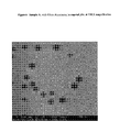
- FIG. 2 GaN by HVPE on Sapphire substrate, at 100 ⁇ magnification.
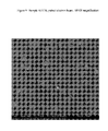
- FIG. 3 Sample B with 100 nm Aluminum at 100 ⁇ magnification.
- FIG. 4 As Grown HVPE GaN layer, Center, 50K ⁇ magnification.
- FIG. 5 As grown HVPE GaN layer, hexagonal pits at 200K ⁇ magnification.
- FIG. 6 Sample A, with 60 nm Aluminum, hexagonal pits, at 73K ⁇ magnification.
- FIG. 7 Sample B9/17, pulsed electron beam spot, 1893 ⁇ magnification.
- FIG. 8 Sample B9/17, pulsed electron beam, 50K ⁇ magnification.
- FIG. 9 Sample A11/20, pulsed electron beam, 1893 ⁇ magnification.
- FIG. 10 Sample A11/20, pulsed electron beam, 50K ⁇ magnification.
- FIG. 11 X Ray Diffraction, as grown HVPE GaN.
- FIG. 12 X Ray Diffraction, Sample A, after 60 nm Aluminum deposition and 10 +16 /cm 2 N+ at 100 KV.
- FIG. 13 X Ray Diffraction, Sample B9/17, HVPE GaN, with 100 nm Al, N+ implanted & twice pulsed electron beam processed.
- FIG. 14 X Ray Diffraction, Sample A11/20, after Al evaporation, N+ implant, twice pulsed electron beam processed.
- the pulsed electron beam process requires a conductive surface in order to be highly uniform. This is done by evaporating a metal such as Aluminum or other Group III metal or a noble metal in the range of a ten to a thousand, or more, nanometers. This also provides the basis to improve the crystallinity of a HVPE GaN substrate.
- a half of a 50 mm O.D HVPE GaN epitaxial layer grown on a polished sapphire wafer was used.
- the half wafer was checked by optical microscopy (FIGS. 2 , 3 ), Scanning Electron Microscopy ( FIG. 4 ) and X Ray Diffraction ( FIG. 11 ). It was diced into four pieces two of which became Samples A and B below for the processing experiments. The other two pieces served as controls.
- the grown layer is epitaxial as a 0002 plane at 36.6 2 theta degrees ( FIG. 11 ).
- This epitaxial layer also shows hexagonal pits of 200-300 nanometers in diameter estimated by the SEM in the 10 +9 /cm 2 range. (FIGS. 5 , 6 ) and the crystallite size is in the 1 to 3 micrometers in diameter.
Landscapes
- Engineering & Computer Science (AREA)
- Physics & Mathematics (AREA)
- Computer Hardware Design (AREA)
- Chemical & Material Sciences (AREA)
- Power Engineering (AREA)
- Microelectronics & Electronic Packaging (AREA)
- Condensed Matter Physics & Semiconductors (AREA)
- General Physics & Mathematics (AREA)
- Manufacturing & Machinery (AREA)
- High Energy & Nuclear Physics (AREA)
- Crystallography & Structural Chemistry (AREA)
- Toxicology (AREA)
- Health & Medical Sciences (AREA)
- Materials Engineering (AREA)
- Electromagnetism (AREA)
- Metallurgy (AREA)
- Organic Chemistry (AREA)
- Optics & Photonics (AREA)
- Inorganic Chemistry (AREA)
- Led Devices (AREA)
- Recrystallisation Techniques (AREA)
- Crystals, And After-Treatments Of Crystals (AREA)
- Physical Deposition Of Substances That Are Components Of Semiconductor Devices (AREA)
Abstract
Gallium Nitride layers grown as single crystals by epitaxy such as Hydride Vapor Phase Epitaxy (HVPE) contain large numbers of crystal defects such as hexagonal pits, which limit the yield and performance of opto- and electronic devices. In this method, the Gallium Nitride layer is first coated with an Aluminum layer of approximate thickness of 0.1 microns. Next, Nitrogen is ion implanted through the Aluminum layer so as to occupy mostly the top 0.1 to 0.5 microns of the Gallium Nitride layer. Finally, through a pulsed directed energy beam such as electron or photons, with a fluence of approximately 1 Joule/cm2 the top approximately 0.5 microns are converted to a single crystal with reduced defect density.
Description
This Utility Application claims the priority benefit of Provisional Patent Application of Dec. 19, 2003, U.S.PTO 60/531,001.
Compound semiconductors of the Groups III-V and II-VI, as well as IV-IV, of the Periodic Chart of the elements, are normally synthesized at high temperatures and even very high pressures, as a boule. Typically at the melting point and standard pressure, the partial pressure of the Group V(or VI) element is high, such that special precautions are required to keep the crystalline imperfections low. For example, in the case of Gallium Arsenide (GaAs) at the melting point of 1238 C., the partial pressure of As over the liquid GaAs is approximately one atmosphere (Reference 1). This is also important in the case of epitaxial layer growth of compound semiconductors, where typical temperatures of 600-1050 C. are used to form many technologically important alloys and devices (Reference 2). Gallium Nitride, has a projected melting point of over 2500 C. with the Nitrogen overpressure of 10 thousand atmospheres (Reference 3).
Compound semiconductors have achieved commercial success during the past twenty years in high brightness Light Emitting Diodes (L.E.D's), for lighting, high performance lasers for optical fiber applications, high efficiency solar cells for satellite power, high speed transistors (in particular Hetero Bipolar Transistors) for cell telephones and other electronic and optoelectronic devices.
Blue LED's and lasers are of particular importance to not only to complete the optical spectrum but for very high density D.V.D and other optical storage applications. A particularly difficult problem for these materials relates to the substrate necessary to grow thin layers that comprise the laser, L.E.D or other electronic or optoelectronic device (Reference 4). The substrate performs several functions from providing the mechanical support, to thermal management, to allowing epitaxy to take place through its crystal structure and dimensions, to being either electrically active through impurity doping or insulating again possibly through impurity doping. Group III-Nitride substrates are the ideal materials for homoepitaxy of these materials. It is known that the growth of large (over a few mm in diameter) single crystal substrates, is extraordinarily difficult to achieve compared to GaAs or InP, for example, which are commercially available to 150 mm Outside Diameter (OD).
This application, in part, relates to one currently available growth process which produces free-standing GaN substrates and is called Hydride Vapor Phase Epitaxy or HVPE (Reference 5). In this process, a sacrificial substrate such as Sapphire, is used to deposit GaN or AlN or their alloys. Inside the apparatus, Group V source elements are carried into a heated zone by using the Group V Hydrides, while for the Group III, a mixture of Hydrogen Chloride in Hydrogen is passed over the Group III metal (e.g Gallium or Aluminum). This process can produce a 100 micron thick substrate in about an hour and easily as large as 75 mm in OD (Reference 5). Typically this type of grown GaN layer contains a very large number of crystalline defects (dislocations) due to the lattice and thermal mismatch. These are seen by a microscope and also revealed through acid etching, as pits, hence, Etch Pit Density (EPD). In this case, the EPD is in the 108 to 1010 per cm2 or even higher.
Ion implantation into a compound semiconductor crystal material is well known that levels in the 10+16/cm2 range and higher will result in an amorphous phase (Reference 6). This amorphous phase will recrystallize into a polycrystalline material at annealing temperatures below 1100 C. It is necessary to anneal out the implantation damage at temperatures exceeding two thirds of the melting point of GaN which is 2518 C. (Reference 7).
Light energy transfer techniques such as from a flash lamp do not produce a fast enough rise in the substrate temperature and are limited to the top temperatures they can achieve to about 1200 C., which is not sufficient to anneal out ion implantation damage of compound semiconductor materials. Directed energy beams such as Pulsed electron beams were used in the past to anneal ion implantation damage in Silicon wafers as large as 100 mm OD. The pulsed electron beam, typically of 0.1 microseconds in duration, produced by an electron gun or a capacitor discharge, is accelerated through a 100 KV field and directed at an optimized angle on the substrate. Alternatively, a pulsed laser, such as a Neodymium pumped YAG laser, is also used. The electron beam total is in the range of 800 to 1000 Amperes and the electrons acquire approximately 10 KeV energy. The pulsed electron beam as above melts the Silicon wafer surface at 1410 C. and the crystallinity of the top micron or so is repaired.
In the case of compound semiconductor materials, a directed energy beam on a non protected surface will result in worse crystallinity due to decomposition.
A method of improving the crystal quality of a Group III Nitride compound semiconductor layer epitaxially grown on a lattice mismatched substrate. The method improvement wherein comprises of: (a) the reduction of surface defects such as hexagonal pits, (b) increase over the as deposited Group III Nitride layer x ray diffraction height and (c) increase in the crystallite size from the as deposited size. The method comprises of the following:
A. Provide said Group III Nitride compound semiconductor epitaxial layer and said layer comprises a top surface;
B. Place said layer of said Group III Nitride compound semiconductor material into an electron beam metal deposition tool and deposit a layer of said Group III metal component upon said top surface;
C. Place said layer of said Group III Nitride compound semiconductor with said deposited layer of said Group III metal component into an ion implantation tool and implant said Nitrogen component into said layers;
D. Place said layer of said Group III Nitride compound semiconductor with said deposited Group III metal layer and said implanted Nitrogen component into a directed pulsed electron beam tool and expose said layers to said pulsed electron beam.
Additionally:
The method above A-D wherein said Group III Nitride compound semiconductor layer is deposited on a sapphire substrate.
The method above A-D wherein said Group III Nitride compound semiconductor layer comprises Gallium Nitride.
The method above A-D, wherein said compound semiconductor layer is deposited by an epitaxial deposition method selected from a group consisting of Hydride Vapor Phase Epitaxy, (HVPE), Metal Organic Vapor Phase Epitaxy (MOVPE), Molecular Beam Epitaxy (MBE) or similar technologies.
The method above A-D wherein said Group III metal component layer comprises Aluminum of approximate thickness 0.1 micrometers.
The method above A-D wherein said Nitrogen ions are implanted at a dose at or below 5expo+16/cm2 so that the Aluminum layer is largely intact in all its properties.
The method above A-D wherein the energy of said implanted Nitrogen component is selected to be sufficient so as to go through said deposited Group III metal component layer and the maximum implanted Nitrogen concentration is inside the Group III compound semiconductor layer below
The method above A-D wherein the amount of said implanted Nitrogen is selected to be sufficient to provide an excess of not yet reacted Nitrogen component into said compound semiconductor layer.
with: The method above A-D wherein said exposing of said layers to said pulsed electron beam occurs under a background gas pressure and wherein said gas comprises Nitrogen or Ammonia gas.
A. The method has three process steps shown as step 2-4. In each of step 2-4, not only is the method detailed but also the end result is shown.
B. The thickness of the layers is not drawn to scale.
C. In Step 4, the Aluminum in Aluminum Gallium Nitride is put in () to indicate that Aluminum is a minor (1 atomic percent or less) component.
D. Gallium Nitride refers not only to Gallium Nitride but also to Group III Nitrides, in the AlGaInN material system.
The pulsed electron beam process requires a conductive surface in order to be highly uniform. This is done by evaporating a metal such as Aluminum or other Group III metal or a noble metal in the range of a ten to a thousand, or more, nanometers. This also provides the basis to improve the crystallinity of a HVPE GaN substrate.
A half of a 50 mm O.D HVPE GaN epitaxial layer grown on a polished sapphire wafer was used. The half wafer was checked by optical microscopy (FIGS. 2,3), Scanning Electron Microscopy (FIG. 4 ) and X Ray Diffraction (FIG. 11 ). It was diced into four pieces two of which became Samples A and B below for the processing experiments. The other two pieces served as controls.
It can be seen by X Ray Diffraction, that the grown layer is epitaxial as a 0002 plane at 36.6 2 theta degrees (FIG. 11 ). This epitaxial layer also shows hexagonal pits of 200-300 nanometers in diameter estimated by the SEM in the 10+9/cm2 range. (FIGS. 5,6) and the crystallite size is in the 1 to 3 micrometers in diameter.
Process I. Pulsed Electron Beam Through Deposited Aluminum Layer:
-
- 1. Deposit a high purity layer of Aluminum metal in the range of 0.06 as Sample A (
FIG. 6 ) and 0.1 micrometers thick, Sample B. This was deposited by electron beam evaporation at a background pressure of 8×10⁻⁶ torr to ensure minimum contamination. Aluminum deposition can also be done by a Chemical Vapor Deposition technique. The use of Aluminum is significant not only because it is a Group III metal and highly conductive but also because a AlGaN alloy can be produced. It is known that the crystal structure and lattice constant of AlN is very similar to GaN and these two are completely miscible in all proportions. Additionally, AlN can be formed afterStep 2 below which is an encapsulating layer. - 2. Implant Nitrogen ions using a Varian model DF3000 ion implantation system. The 14N+ beam was derived from Nitrogen gas in a hot filament ion source and analyzed magnetically. The N+ ions were accelerated through a 100 KV potential and then scanned across the sample electrostatically. The 100 KV is chosen to allow the majority of Nitrogen ions to go through the Aluminum layer and occupy the top 0.2 microns of the Gallium Nitride layer. Additionally, as the Nitrogen is implanted through the Aluminum layer an Aluminum Nitride layer is formed at the relatively high dose used of 5×10+16/cm2. The samples marked A and B were not cooled. Above 10+16/cm2 an amorphous and porous layer forms (Reference 6)_which is normally highly undesirable because can not be annealed completely back to single crystal. The X Ray Diffraction shows a much reduced and wider 0002 plane peak confirming an amorphous layer was formed (
FIG. 12 ) with very low peak intensity. - 3. Next a pulsed electron beam generated by Electron Gun, such as in a Neocera Pulsed Electron Beam deposition system modified by defocusing the electron beam used (Reference 8). Irradiation of each of the samples is made with single pulse of energetic electrons, at room temperature. The sample is attached to a non-grounded metallic holder. The distance between the electron source and the sample is 15 mm and the average beam diameter on sample surface is 3-4 mm. The samples A and B were further diced into four pieces each to allow for a control as well as different fluence levels. The electric field of 9 to 20 KV is used, and up to 1KA, only limited by the power supply and with a typical pulse width of 150 nanoseconds, resulting in an energy fluence from 0.1 to 1 Joules per cm2 (Table 1). The electron beam pulse was repeated for two samples A11/20 and B9/17 as necessary to optimize the results. The samples now show a recrystalized area surrounded by the metallized front of the wafers. The twice pulsed samples A11/20 and B9/17 show a further improvement in peak height and peak half width as seen in Table 2.
- 1. Deposit a high purity layer of Aluminum metal in the range of 0.06 as Sample A (
| TABLE 1 |
| Pulsed Electron Beam experiments summary |
| Peak | Average | ||||
| Source | beam | electron | Pulse | ||
| Voltage, | current, | energy, | duration, | Pressure, | |
| Sample | kV | Amperes | KeV | nanoseconds | mTorr |
| A9/17 | 9 and 17 | 700 | 8.5 | 150 | 9.5 |
| B9/17 | 9 and 17 | 700 | 8.5 | 150 | 9.5 |
| A11/20 | 11 and 20 | 850 | 10 | 150 | 9.0 |
| B11/20 | 11 and 20 | 850 | 10 | 150 | 9.0 |
| A14 | 14 | 700 | 8.5 | 150 | 9.5 |
| B14 | 14 | 850 | 10 | 150 | 9.0 |
-
- 4. Next, X Ray Diffraction is used to check the affects of the processing. A Rigaku DMAX“A” instrument is used. The radiation is Cu K alpha, Nickel filtered, the anode operating at 20 KV and 2 mA. The scans are made from 20 to 90 2 theta degrees. The only major peak is the 0002 at 36.6, 2 theta degrees, confirming the strong epitaxy. After N+ implantation the peak height decreases significantly, which the recovers at the various fluence levels. This is summarized in Table 2. Clearly the implantation damage is relieved which confirms the very high temperature achieved. More significantly, the much increased peak height of the 0002 peak for Samples B9/17 and A11/20, indicating the improvement that can be achieved (Table 2).
- 5. Finally, a Hitachi S-3500N Scanning Electron Microscope is used to look at surface defects. Several magnifications were used and the 50K× is used for comparisons. The operating electron voltage is 30 KV and the instrument pressure is 133.3 Pa. Hexagonal pits form as Gallium Nitride is known to grow as pyramids and where the pyramids coalesce, a pit forms. These pits are seen by the SEM and are 200-300 nanometers across and estimated in the 10+9/cm2 range. Significantly, after processing the pit density is clearly lower by over an order of magnitude a seen in Table 2. Additionally, the crystallite size increases to 5-10 micrometers as seen in Sample B9/17, by the SEM (
FIG. 7 ).
| TABLE 2 |
| X Ray Diffraction and SEM summary |
| 2Theta | Peak Height | FWHM | Crystal O.D(SEM) | ||
| Sample | History | Degrees | (Arbitr. Units) | Degrees | Micrometers |
| HVPE | As grown | 34.661 | 280 | 0.238 | 1-3 |
| A | 60 nm Al | ||||
| N+ implanted | 34.661 | 10 | 0.238 | 1-3 | |
| A14 | Same as A | 34.593 | 387 | 0.387 | |
| Pulsed Electron Beam | |||||
| One pulse | |||||
| A11/20 | 60 nm Al | 34.596 | 1008 | 0.312 | 5-10 |
| N+ implanted | |||||
| Pulsed Electron beam | |||||
| Twice pulsed | |||||
| |
100 nm Al | 34.573 | 492 | 0.387 | |
| Pulsed Electron Beam | |||||
| One pulse | |||||
| B9/17 | 100 nm Al | 34.577 | 1220 | 0.271 | 5-10 |
| N+ implanted | |||||
| Pulsed electron beam | |||||
| Twice pulsed | |||||
-
- 1. This application, in part, relates to one currently available growth process which produces free-standing GaN substrates and is called Hydride Vapor Phase Epitaxy or HVPE rather than on the more common crystal growth techniques where a boule is produced under the appropriate temperature and pressure from the compound elements. Since in HVPE the layer is grown on a non GaN substrate, as it is not available in standard size, a lattice mismatched material, the crystal defects are very large in number, i.e. 10+8-10+10 cm2. The result is, must be used. In the case when epitaxy is required to grow Group III-Nitride devices such as lasers, the yields are very poor. A reduction by at least two orders of magnitude is necessary to produce commercially useful substrates of this type.
- 2. The use of excess Aluminum as an encapsulating layer is important in several ways. First, it is necessary to spread out the electron beam. Second it is sacrificial and can be sputtered off during N+ implantation or blown off by pulsed energy beam. Third it can be reacted out to an Aluminum Nitride or a mixed Aluminum Gallium Nitride alloy. Fourth, during the N+ implantation, the substrate may heated to about 500 C., which reduces the radiation damage. And, Fifth, the use of the Aluminum layer effectively slows down the implanted Nitrogen ions and thus the radiation damage is minimized. Aluminum is preferred over Gallium because Gallium has a very low melting point, but Aluminum is completely acceptable and preferable as explained above. The result is the new surface generated at the top of the GaN layer after processing, shows improved crystallinity as seen by Scanning Electron Microscopy and by the increased X Ray peak height of the 0002 plane (Table 2 and FIGS. 13,14). This makes the layer more suitable for higher yield of blue/green laser devices by layer deposition.
- 3. The use of ion implantation is standard in semiconductor technology. However, it is also well known that radiation damage due to high energy of the implantation process requires a high enough temperature to anneal out, which is estimated at ⅔ of the melting point (Reference 7). In the case of Gallium Nitride that is around 1650 Celcius. Additionally, N+ implantation may result in a porous, amorphous material with gaseous inclusions due to decomposition and therefore not obvious. Even higher levels of N+ implantation may result in a higher concentration of interstitial Nitrogen, which would produce a higher Nitrogen overpressure which is necessary to anneal out the defects to a greater degree but at an even greater temperature. The use of Nitrogen is then necessary to promote a chemical reaction and alloying with the existing GaN layer and deposited Aluminum and thus a novel approach.
- 4. Given that these compound semiconductors are sensitive and prone to decomposition at higher than ambient temperatures, any technique which can improve the EPD of grown wafers as compared to a boule, needs to be very fast, at sub microsecond length, such as the pulsed electron or laser techniques.
- 5. In the case of ion implantation damage, a directed energy beam such as a pulsed electron beam has been demonstrated to anneal out the damage, at the appropriate energy level or fluence, as energy per cm2. The voltage used as well as the energy fluence, in Joules per cm2, affect the charachteristics of the beam such as surface penetration. Additionally, the beam must be controlled to be as uniform as possible to achieve uniformity of heating and thus crystallinity repair. The fluence required for this application is in the order of 1 Joule per cm2.
- 6. When the pulsed electron beam is highly focused, such as approximately 1 mm2, the highly focused beam can lead to very rapid and localized temperature rise and thus to vaporization and consequently deposition of the target material on a substrate (Reference 8). In this patent application, a defocused beam of the necessary fluence, is required to produce annealing and reaction to relieve the radiation damage on a larger scale and be of commercial value. The result of the directed energy beam such as the pulsed electron beam is to raise the surface temperature from ambient to well over 1000 C. depending on the fluence and other factors such as energy coupling to the surface. As the surface temperature rises by the energy transfer, the Aluminum atoms from the melted Aluminum layer on the surface, into the underlying material. In this case, Aluminum, given its reactivity, can alloy with the Gallium Nitride substrate material and in the process compress the interstitial Nitrogen to very high pressure and temperature. Since the pulse is sufficiently short, decomposition does not occur and is further controlled by the capping Aluminum Nitride and Aluminum layer. The resulting AlGaN alloy as seen from Table 2, where the 2 theta is reduced and thus the lattice spacing is reduced towards that of Aluminum Nitride. This AlGaN alloy formed from the surface to some depth, is now of lower EPD as a result of filling the voids and other defects and defect annihilation by solid state diffusion, alloying and very high temperature and pressure. This is effectively a surface polishing technique as well.
- 7. By use of multiple directed energy pulses, the temperature rise as well as depth of Aluminum diffusion, increase. This leads to greater defect annihilation as is seen in Table 2. The crystallite size increases by several fold and the X Ray Diffraction half width decreases compared to the single pulsed layers.
While the invention has been described in terms of certain preferred embodiments, modifications obvious to with ordinary skill in the art may be made without departing from the scope of the invention.
Claims (14)
1. A method of improving the crystal quality of a Group III Nitride compound semiconductor layer epitaxially grown on a lattice mismatched substrate comprising:
A. providing said Group III Nitride compound semiconductor epitaxial layer and said Group III Nitride compound semiconductor epitaxial layer comprises a top surface;
B. placing said layer of said Group III Nitride compound semiconductor material into an electron beam metal deposition tool and depositing a layer of Group III metal component upon said top surface;
C. placing said layer of said Group III Nitride compound semiconductor with said deposited layer of said Group III metal component into an ion implantation tool and implanting a Nitrogen component through said Group metal component layer into said Group III Nitride compound semiconductor epitaxial layer, thereby forming a Group III Nitride compound semiconductor layer with an excess of unreacted nitrogen;
D. placing said layer of said Group III Nitride compound semiconductor with said deposited Group III metal layer and said implanted Nitrogen component into a directed pulsed electron beam tool and exposing said layers to a pulsed electron beam;
wherein said Group III Nitride compound semiconductor layer after exposure to said pulsed electron beam exhibits a reduction of hexagonal pits, an increase in x ray diffraction height and an increase in the crystallite size compared to the as deposited Group III Nitride compound semiconductor layer.
2. The method of claim 1 wherein said Group III Nitride compound semiconductor layer is deposited on a sapphire substrate.
3. The method of claim 1 wherein said Group III Nitride compound semiconductor layer comprises Gallium Nitride.
4. The method of claim 1 wherein said epitaxial deposition method is selected from a group consisting of Hydride Vapor Phase Epitaxy, (HVPE), metalorganic vapor phase epitaxy (MOVPE), and molecular beam epitaxy (MBE) or similar technologies.
5. The method of claim 1 wherein said Group III metal component layer comprises Aluminum of approximate thickness 0.1 micrometers.
6. The method of claim 1 wherein said implanted of Nitrogen ions at a dose at or below 5expo+16/cm2 so that the Aluminum layer largely intact in all its properties.
7. The method of claim 1 wherein the energy of said implanted Nitrogen component is selected to be sufficient so as to go through said deposited Group III metal component layer and the maximum implanted Nitrogen concentration is inside the Group III compound semiconductor layer below.
8. The method of claim 1 wherein said pulsed energy beam comprises an energy to raise the surface temperature to effect crystal quality improvement of between 0.1 and 2 Joule per cm2.
9. The method of claim 1 wherein said pulsed energy beam comprises of a pulse duration of less than a microsecond.
10. The method of claim 1 wherein said pulsed electron beam comprises a diameter of at least 3 mm.
11. The method of claim 1 wherein said exposing of said layers to said pulsed electron beam occurs under a background gas pressure and wherein said gas comprises Nitrogen or Ammonia gas.
12. The method of claim 1 wherein said pulsed energy beam is used more than one time sequentially.
13. The method of claim 1 , wherein said pulsed energy beam is moved in a controlled manner over the entire surface of said layers.
14. The method of claim 1 , wherein said pulsed electron beam is stationary and said layers are exposed to said beam by moving said layers in a controlled manner.
Priority Applications (2)
| Application Number | Priority Date | Filing Date | Title |
|---|---|---|---|
| US11/014,304 US7341628B2 (en) | 2003-12-19 | 2004-12-16 | Method to reduce crystal defects particularly in group III-nitride layers and substrates |
| US11/998,961 US20080087984A1 (en) | 2003-12-19 | 2007-12-03 | Compound semiconductor modified surface by use of pulsed electron beam and ion implantation through a deposited metal layer |
Applications Claiming Priority (2)
| Application Number | Priority Date | Filing Date | Title |
|---|---|---|---|
| US53100103P | 2003-12-19 | 2003-12-19 | |
| US11/014,304 US7341628B2 (en) | 2003-12-19 | 2004-12-16 | Method to reduce crystal defects particularly in group III-nitride layers and substrates |
Related Child Applications (1)
| Application Number | Title | Priority Date | Filing Date |
|---|---|---|---|
| US11/998,961 Division US20080087984A1 (en) | 2003-12-19 | 2007-12-03 | Compound semiconductor modified surface by use of pulsed electron beam and ion implantation through a deposited metal layer |
Publications (2)
| Publication Number | Publication Date |
|---|---|
| US20050136627A1 US20050136627A1 (en) | 2005-06-23 |
| US7341628B2 true US7341628B2 (en) | 2008-03-11 |
Family
ID=34680921
Family Applications (2)
| Application Number | Title | Priority Date | Filing Date |
|---|---|---|---|
| US11/014,304 Expired - Fee Related US7341628B2 (en) | 2003-12-19 | 2004-12-16 | Method to reduce crystal defects particularly in group III-nitride layers and substrates |
| US11/998,961 Abandoned US20080087984A1 (en) | 2003-12-19 | 2007-12-03 | Compound semiconductor modified surface by use of pulsed electron beam and ion implantation through a deposited metal layer |
Family Applications After (1)
| Application Number | Title | Priority Date | Filing Date |
|---|---|---|---|
| US11/998,961 Abandoned US20080087984A1 (en) | 2003-12-19 | 2007-12-03 | Compound semiconductor modified surface by use of pulsed electron beam and ion implantation through a deposited metal layer |
Country Status (1)
| Country | Link |
|---|---|
| US (2) | US7341628B2 (en) |
Cited By (4)
| Publication number | Priority date | Publication date | Assignee | Title |
|---|---|---|---|---|
| US20080069753A1 (en) * | 2006-09-15 | 2008-03-20 | Cabot Corporation | Method of preparing hydrophobic silica |
| US20090178276A1 (en) * | 2008-01-16 | 2009-07-16 | Fukui Precision Component (Shenzhen) Co., Ltd. | Method for forming circuit in making printed circuit board |
| US8110424B2 (en) | 2008-10-14 | 2012-02-07 | Samsung Led Co., Ltd. | Surface treatment method of group III nitride semiconductor and manufacturing method of the group III nitride semiconductor |
| US20140073095A1 (en) * | 2007-02-27 | 2014-03-13 | Sanken Electric Co., Ltd. | High electron mobility transistor and method of forming the same |
Families Citing this family (19)
| Publication number | Priority date | Publication date | Assignee | Title |
|---|---|---|---|---|
| US8545629B2 (en) | 2001-12-24 | 2013-10-01 | Crystal Is, Inc. | Method and apparatus for producing large, single-crystals of aluminum nitride |
| JP4620333B2 (en) * | 2003-05-09 | 2011-01-26 | 三菱電機株式会社 | Manufacturing method of semiconductor device |
| US7641735B2 (en) * | 2005-12-02 | 2010-01-05 | Crystal Is, Inc. | Doped aluminum nitride crystals and methods of making them |
| US9034103B2 (en) * | 2006-03-30 | 2015-05-19 | Crystal Is, Inc. | Aluminum nitride bulk crystals having high transparency to ultraviolet light and methods of forming them |
| CN107059116B (en) | 2007-01-17 | 2019-12-31 | 晶体公司 | Defect reduction in seeded aluminum nitride crystal growth |
| US9771666B2 (en) | 2007-01-17 | 2017-09-26 | Crystal Is, Inc. | Defect reduction in seeded aluminum nitride crystal growth |
| US8080833B2 (en) | 2007-01-26 | 2011-12-20 | Crystal Is, Inc. | Thick pseudomorphic nitride epitaxial layers |
| US8395132B2 (en) | 2007-06-25 | 2013-03-12 | International Rectifier Corporation | Ion implanting while growing a III-nitride layer |
| US9218991B2 (en) | 2007-06-25 | 2015-12-22 | Infineon Technologies Americas Corp. | Ion implantation at high temperature surface equilibrium conditions |
| EP2588651B1 (en) | 2010-06-30 | 2020-01-08 | Crystal Is, Inc. | Growth of large aluminum nitride single crystals with thermal-gradient control |
| JP4948629B2 (en) * | 2010-07-20 | 2012-06-06 | ウシオ電機株式会社 | Laser lift-off method |
| US8962359B2 (en) | 2011-07-19 | 2015-02-24 | Crystal Is, Inc. | Photon extraction from nitride ultraviolet light-emitting devices |
| US20130056793A1 (en) * | 2011-09-07 | 2013-03-07 | Applied Materials, Inc. | Providing group v and group vi over pressure for thermal treatment of compound semiconductor thin films |
| TW201314924A (en) * | 2011-09-22 | 2013-04-01 | Pinecone En Inc | Method of making a solar cell and a structure thereof |
| JP2014146748A (en) * | 2013-01-30 | 2014-08-14 | Toshiba Corp | Semiconductor device, method of manufacturing the same, and semiconductor substrate |
| EP2765596B1 (en) * | 2013-02-12 | 2018-07-11 | Infineon Technologies Americas Corp. | Ion implantation at high temperature surface equilibrium conditions |
| JP6275817B2 (en) | 2013-03-15 | 2018-02-07 | クリスタル アイエス, インコーポレーテッドCrystal Is, Inc. | Planar contacts to pseudomorphic and optoelectronic devices |
| FR3086097B1 (en) * | 2018-09-18 | 2020-12-04 | Commissariat Energie Atomique | METHOD FOR MANUFACTURING AN ELECTROLUMINESCENT DEVICE |
| WO2021026530A1 (en) * | 2019-08-08 | 2021-02-11 | The Regents Of The University Of California | Crystallization of two-dimensional structures comprising multiple thin films |
Citations (4)
| Publication number | Priority date | Publication date | Assignee | Title |
|---|---|---|---|---|
| US4151008A (en) * | 1974-11-15 | 1979-04-24 | Spire Corporation | Method involving pulsed light processing of semiconductor devices |
| US4154625A (en) * | 1977-11-16 | 1979-05-15 | Bell Telephone Laboratories, Incorporated | Annealing of uncapped compound semiconductor materials by pulsed energy deposition |
| US6358766B1 (en) * | 1999-06-22 | 2002-03-19 | Semiconductor Energy Laboratory Co., Ltd. | Method of fabricating a semiconductor device |
| US20020164852A1 (en) * | 2001-01-05 | 2002-11-07 | Leonard Forbes | Capacitor structures |
Family Cites Families (10)
| Publication number | Priority date | Publication date | Assignee | Title |
|---|---|---|---|---|
| US5578839A (en) * | 1992-11-20 | 1996-11-26 | Nichia Chemical Industries, Ltd. | Light-emitting gallium nitride-based compound semiconductor device |
| US5656832A (en) * | 1994-03-09 | 1997-08-12 | Kabushiki Kaisha Toshiba | Semiconductor heterojunction device with ALN buffer layer of 3nm-10nm average film thickness |
| US5740192A (en) * | 1994-12-19 | 1998-04-14 | Kabushiki Kaisha Toshiba | Semiconductor laser |
| US5670798A (en) * | 1995-03-29 | 1997-09-23 | North Carolina State University | Integrated heterostructures of Group III-V nitride semiconductor materials including epitaxial ohmic contact non-nitride buffer layer and methods of fabricating same |
| US5679965A (en) * | 1995-03-29 | 1997-10-21 | North Carolina State University | Integrated heterostructures of Group III-V nitride semiconductor materials including epitaxial ohmic contact, non-nitride buffer layer and methods of fabricating same |
| US5625202A (en) * | 1995-06-08 | 1997-04-29 | University Of Central Florida | Modified wurtzite structure oxide compounds as substrates for III-V nitride compound semiconductor epitaxial thin film growth |
| JPH0964477A (en) * | 1995-08-25 | 1997-03-07 | Toshiba Corp | Semiconductor light emitting element and its manufacture |
| JP3409958B2 (en) * | 1995-12-15 | 2003-05-26 | 株式会社東芝 | Semiconductor light emitting device |
| US6599133B2 (en) * | 1997-11-18 | 2003-07-29 | Technologies And Devices International, Inc. | Method for growing III-V compound semiconductor structures with an integral non-continuous quantum dot layer utilizing HVPE techniques |
| US6090300A (en) * | 1998-05-26 | 2000-07-18 | Xerox Corporation | Ion-implantation assisted wet chemical etching of III-V nitrides and alloys |
-
2004
- 2004-12-16 US US11/014,304 patent/US7341628B2/en not_active Expired - Fee Related
-
2007
- 2007-12-03 US US11/998,961 patent/US20080087984A1/en not_active Abandoned
Patent Citations (4)
| Publication number | Priority date | Publication date | Assignee | Title |
|---|---|---|---|---|
| US4151008A (en) * | 1974-11-15 | 1979-04-24 | Spire Corporation | Method involving pulsed light processing of semiconductor devices |
| US4154625A (en) * | 1977-11-16 | 1979-05-15 | Bell Telephone Laboratories, Incorporated | Annealing of uncapped compound semiconductor materials by pulsed energy deposition |
| US6358766B1 (en) * | 1999-06-22 | 2002-03-19 | Semiconductor Energy Laboratory Co., Ltd. | Method of fabricating a semiconductor device |
| US20020164852A1 (en) * | 2001-01-05 | 2002-11-07 | Leonard Forbes | Capacitor structures |
Non-Patent Citations (3)
| Title |
|---|
| Geppert, L., "The Great Gallium Nitride Gamble", IEEE Spectrum, Jan. 2004, pp. 52-59. |
| Patent Abstracts of Japan. English Abstract of JP 61-251599 (1986). * |
| Tan, H.,H., et.al., " Annealing of ion implanted gallium nitride", Applied Physics Letters, V. 72, No. 10, pp. 1190-1192, 1998. |
Cited By (5)
| Publication number | Priority date | Publication date | Assignee | Title |
|---|---|---|---|---|
| US20080069753A1 (en) * | 2006-09-15 | 2008-03-20 | Cabot Corporation | Method of preparing hydrophobic silica |
| US20140073095A1 (en) * | 2007-02-27 | 2014-03-13 | Sanken Electric Co., Ltd. | High electron mobility transistor and method of forming the same |
| US20090178276A1 (en) * | 2008-01-16 | 2009-07-16 | Fukui Precision Component (Shenzhen) Co., Ltd. | Method for forming circuit in making printed circuit board |
| US8110424B2 (en) | 2008-10-14 | 2012-02-07 | Samsung Led Co., Ltd. | Surface treatment method of group III nitride semiconductor and manufacturing method of the group III nitride semiconductor |
| US8476639B2 (en) | 2008-10-14 | 2013-07-02 | Samsung Electronics Co., Ltd. | Group III nitride semiconductor and group III nitride semiconductor structure |
Also Published As
| Publication number | Publication date |
|---|---|
| US20050136627A1 (en) | 2005-06-23 |
| US20080087984A1 (en) | 2008-04-17 |
Similar Documents
| Publication | Publication Date | Title |
|---|---|---|
| US7341628B2 (en) | Method to reduce crystal defects particularly in group III-nitride layers and substrates | |
| EP0551721B1 (en) | Gallium nitride base semiconductor device and method of fabricating the same | |
| JP5033279B2 (en) | Zinc oxide film containing P-type dopant and method for producing the same | |
| JP4716526B2 (en) | Method for producing semiconductor device by exposing sapphire substrate to active nitrogen and semiconductor device | |
| US7033435B2 (en) | Process for preparing p-n junctions having a p-type ZnO film | |
| US4863877A (en) | Ion implantation and annealing of compound semiconductor layers | |
| US5602418A (en) | Nitride based semiconductor device and manufacture thereof | |
| US5998232A (en) | Planar technology for producing light-emitting devices | |
| EP1296363B1 (en) | Method of manufacturing group-iii nitride compound semiconductor device | |
| US7964868B2 (en) | Semiconductor light-emitting device and method of manufacturing the same | |
| US8097482B2 (en) | Method for manufacturing group III nitride semiconductor, method for manufacturing group III nitride semiconductor light-emitting device, group III nitride semiconductor light-emitting device, and lamp | |
| US6995398B2 (en) | Methods of treating a silicon carbide substrate for improved epitaxial deposition and resulting structures and devices | |
| Lin et al. | Synthesis of GaN by N ion implantation in GaAs (001) | |
| US20060246614A1 (en) | Method for manufacturing gallium nitride-based semiconductor device | |
| JPH09266218A (en) | Method to reduce resistance of p-type compound semiconductor | |
| JPH1070082A (en) | Method of forming p-type nitride based iii-v compound semiconductor layer | |
| US11600496B2 (en) | In-situ p-type activation of III-nitride films grown via metal organic chemical vapor deposition | |
| JP2002261024A (en) | Nitride semiconductor epitaxial wafer and its manufacturing method, and semiconductor device | |
| CN1140919C (en) | Activation method for reducing p type film resistance by laser | |
| JPH0376169A (en) | Manufacture of electronic device using diamond | |
| CN117013361A (en) | Ohmic contact generation method based on P-type gallium nitride and semiconductor device | |
| CN1372305A (en) | Method for activating high-resistance P type doping film into low-resistance P type doping film |
Legal Events
| Date | Code | Title | Description |
|---|---|---|---|
| REMI | Maintenance fee reminder mailed | ||
| LAPS | Lapse for failure to pay maintenance fees | ||
| STCH | Information on status: patent discontinuation |
Free format text: PATENT EXPIRED DUE TO NONPAYMENT OF MAINTENANCE FEES UNDER 37 CFR 1.362 |
|
| FP | Expired due to failure to pay maintenance fee |
Effective date: 20120311 |