US7277217B1 - Optical deflecting device, optical deflecting device manufacturing method, and optical projecting device - Google Patents

Optical deflecting device, optical deflecting device manufacturing method, and optical projecting device Download PDF

Info

Publication number
US7277217B1
US7277217B1 US11/681,021 US68102107A US7277217B1 US 7277217 B1 US7277217 B1 US 7277217B1 US 68102107 A US68102107 A US 68102107A US 7277217 B1 US7277217 B1 US 7277217B1
Authority
US
United States
Prior art keywords
plate
shaped member
bearing portion
deflecting device
optical deflecting
Prior art date
Legal status (The legal status is an assumption and is not a legal conclusion. Google has not performed a legal analysis and makes no representation as to the accuracy of the status listed.)
Expired - Fee Related
Application number
US11/681,021
Other versions
US20070206268A1 (en
Inventor
Seiichi Katoh
Takeshi Nanjyo
Koichi Ohtaka
Current Assignee (The listed assignees may be inaccurate. Google has not performed a legal analysis and makes no representation or warranty as to the accuracy of the list.)
Ricoh Co Ltd
Original Assignee
Ricoh Co Ltd
Priority date (The priority date is an assumption and is not a legal conclusion. Google has not performed a legal analysis and makes no representation as to the accuracy of the date listed.)
Filing date
Publication date
Application filed by Ricoh Co Ltd filed Critical Ricoh Co Ltd
Assigned to RICOH COMPANY, LTD. reassignment RICOH COMPANY, LTD. ASSIGNMENT OF ASSIGNORS INTEREST (SEE DOCUMENT FOR DETAILS). Assignors: KATOH, SEIICHI, Nanjyo, Takeshi, Ohtaka, Koichi
Publication of US20070206268A1 publication Critical patent/US20070206268A1/en
Application granted granted Critical
Publication of US7277217B1 publication Critical patent/US7277217B1/en
Expired - Fee Related legal-status Critical Current
Anticipated expiration legal-status Critical

Links

Images

Classifications

    • GPHYSICS
    • G02OPTICS
    • G02BOPTICAL ELEMENTS, SYSTEMS OR APPARATUS
    • G02B26/00Optical devices or arrangements for the control of light using movable or deformable optical elements
    • G02B26/08Optical devices or arrangements for the control of light using movable or deformable optical elements for controlling the direction of light
    • G02B26/0816Optical devices or arrangements for the control of light using movable or deformable optical elements for controlling the direction of light by means of one or more reflecting elements
    • G02B26/0833Optical devices or arrangements for the control of light using movable or deformable optical elements for controlling the direction of light by means of one or more reflecting elements the reflecting element being a micromechanical device, e.g. a MEMS mirror, DMD
    • G02B26/0841Optical devices or arrangements for the control of light using movable or deformable optical elements for controlling the direction of light by means of one or more reflecting elements the reflecting element being a micromechanical device, e.g. a MEMS mirror, DMD the reflecting element being moved or deformed by electrostatic means

Definitions

  • the present invention relates to an optical deflecting device that changes the direction of output light with respect to incident light and a method of manufacturing such an optical deflecting device, and also relates a technology suitable for image forming apparatuses, such as electrophotographic printers and copiers, and projection-type image and vide display apparatuses, such as projectors and digital theater systems.
  • image forming apparatuses such as electrophotographic printers and copiers, and projection-type image and vide display apparatuses, such as projectors and digital theater systems.
  • a hinge In these micromirror devices, mirrors are generally supported by a torsion beam called a hinge. By using the hinge, the reflection area is reduced.
  • a DMD from Texas Instruments Incorporated has a two-storied structure provided with a reflecting member on the surface separately from the hinge portion.
  • the actual voltage to be driven is as much as several tens of volts.
  • a bias voltage of several tens of volts to be applied all at one to a plurality of pixels and a restoring force of a special spring member are combined to switch the tilt.
  • the optical deflecting device includes a substrate, a plurality of regulating members, a pivot member, and a plate-shaped member.
  • the regulating members each has a stopper on an upper portion and are provided to a plurality of ends.
  • the pivot member has an apex formed of a conductive material and is provided on an upper surface of the substrate.
  • the plate-shaped member does not have a fixed end, has the light reflecting area on an upper surface, and at least partially has a conductive material layer formed of a conductive member. At least a contact point making contact with the apex on a back surface is formed of a conductive member.
  • the plate-shaped member is movably disposed within a space formed of the substrate, the pivot member, and the stopper, and provides a potential of the plate-shaped member through a contact with the pivot member (refer to Japanese Patent Application Laid-Open No. 2004-78136).
  • the driving voltage is high, as much as several tens of volts.
  • high-definition and high-resolution television for example, high-definition and high-resolution is required, and the number of pixels tend to be increased.
  • the chip size is expanded. In that case, a special process is required, and material cost is increased.
  • the mirror dimension forming a pixel is required to be decreased. With this, the stiffness of the hinge hanging the mirror is increased, thereby increasing the driving voltage. For further downsizing, it is not easy to decrease the stiffness of the hinge because of limitations of microfabrication accuracy for making the hinge narrower.
  • the hinge is bent, and cannot sustain the center position of the mirror.
  • the hinge is formed on the surface, and therefore the area that reflects light is decreased.
  • a complex structure has to be adopted in which a reflecting surface is formed on a driving electrode hanged by the hinge to form a double structure so as to increase the reflecting area.
  • a post is formed to superpose the mirror on the electrode, but since the post has a hole, the mirror inevitably has an area where light cannot be reflected, thereby inviting a decrease in reflection efficiency. From these reason above, in the structure using a hinge, there is a problem in which downsizing results in a complex element structure and high manufacturing cost.
  • an optical deflecting device includes a substrate; a pivot member formed on the substrate; a regulating member formed on the substrate; a plate-shaped member having an upper surface as a light reflecting surface; and a group of electrodes formed on the substrate.
  • the plate-shaped member has a loop-shaped bearing portion on a lower surface side
  • the regulating member has a stopper protruding in approximately parallel to the substrate and embedded inside the bearing portion, with an engagement of the lower surface of the plate-shaped member and an apex of the pivot member and an engagement of an inner surface of the bearing portion and a lower surface of the stopper, the plate-shaped member is rotatably supported with the apex of the pivot member as a center, and a position of the plate-shaped member in a rotation axis direction is regulated by a side surface of the regulating member facing a side surface of the bearing portion, and with an electrostatic force generated between the group of electrodes and the plate-shaped member, the plate-shaped member is rotated with the apex of the pivot member as the center, thereby changing a reflecting direction of a light beam incident to the light reflecting surface of the plate-shaped member.
  • a method of manufacturing the optical deflecting device includes, after planarizing a photoresist serving as a sacrifice layer, forming a concave surface corresponding to the bearing portion through etching process; next forming a film made of a material serving as the lower layer of the plate-shaped member; next forming and patterning a sacrifice layer along the concave surface; and next forming a film serving as the stopper of the regulating member.
  • an optical projecting device includes the above optical deflecting device; a light source that light up a light reflecting surface of a plate-shaped member of the optical deflecting device; and an optical system that projects light reflected from the light reflecting surface when the plate-shaped member of the optical deflecting device is tilted in a first tilting direction, and shields light reflected from the light reflecting surface and prevents the light from being projected outside when the plate-shaped member is tilted in a second tilting direction.
  • FIGS. 1A to 1D are drawings of the structure of an optical deflecting device according to a first embodiment of the present invention
  • FIG. 2 is a drawing for explaining a rotational supporting structure of a plate-shaped member
  • FIGS. 3A and 3B are drawings for explaining an optical deflecting device manufacturing method according to the first embodiment
  • FIG. 4 is a drawing for explaining continuation of the manufacturing method shown in FIG. 3B ;
  • FIG. 5 is a drawing for explaining continuation of the manufacturing method shown in FIG. 4 ;
  • FIG. 6 is a drawing for explaining continuation of the manufacturing method shown in FIG. 5 ;
  • FIG. 7 is a drawing for explaining continuation of the manufacturing method shown in FIG. 6 ;
  • FIG. 8 is a drawing for explaining continuation of the manufacturing method shown in FIG. 7 ;
  • FIG. 9 is a drawing for explaining continuation of the manufacturing method shown in FIG. 8 ;
  • FIG. 10 is a drawing for explaining continuation of the manufacturing method shown in FIG. 9 ;
  • FIG. 11 is a drawing for explaining continuation of the manufacturing method shown in FIG. 10 ;
  • FIG. 12 is a drawing for explaining continuation of the manufacturing method shown in FIG. 11 ;
  • FIGS. 13A to 13D are drawings of the structure of an optical deflecting device according to a second embodiment of the present invention.
  • FIGS. 14A and 14B are drawings for explaining an optical deflecting device manufacturing method according to the second embodiment
  • FIG. 15 is a drawing for explaining continuation of the manufacturing method shown in FIG. 14B ;
  • FIG. 16 is a drawing for explaining continuation of the manufacturing method shown in FIG. 15 ;
  • FIG. 17 is a drawing for explaining continuation of the manufacturing method shown in FIG. 16 ;
  • FIG. 18 is a drawing for explaining continuation of the manufacturing method shown in FIG. 17 ;
  • FIG. 19 is a drawing for explaining continuation of the manufacturing method shown in FIG. 18 ;
  • FIG. 20 is a drawing for explaining continuation of the manufacturing method shown in FIG. 19 ;
  • FIG. 21 is a drawing for explaining continuation of the manufacturing method shown in FIG. 20 ;
  • FIG. 22 is a drawing for explaining continuation of the manufacturing method shown in FIG. 21 ;
  • FIG. 23 is a drawing for explaining continuation of the manufacturing method shown in FIG. 22 ;
  • FIGS. 24A to 24D are drawings of the structure of an optical deflecting device according to a third embodiment of the present invention.
  • FIGS. 25A and 25B are drawings for explaining an optical deflecting device according to the third embodiment
  • FIG. 26 is a drawing for explaining continuation of the manufacturing method shown in FIG. 25B ;
  • FIG. 27 is a drawing for explaining continuation of the manufacturing method shown in FIG. 26 ;
  • FIG. 28 is a drawing for explaining continuation of the manufacturing method shown in FIG. 27 ;
  • FIG. 29 is a drawing for explaining continuation of the manufacturing method shown in FIG. 28 ;
  • FIG. 30 is a drawing for explaining continuation of the manufacturing method shown in FIG. 29 ;
  • FIG. 31 is a drawing for explaining continuation of the manufacturing method shown in FIG. 30 ;
  • FIG. 32 is a drawing for explaining continuation of the manufacturing method shown in FIG. 31 ;
  • FIG. 33 is a drawing for explaining continuation of the manufacturing method shown in FIG. 32 ;
  • FIG. 34 is a drawing for explaining continuation of the manufacturing method shown in FIG. 33 ;
  • FIG. 35 is a schematic drawing of an optical projecting device according to a fourth embodiment of the present invention.
  • FIGS. 1A to 1D and 2 are drawings of the structure of an optical deflecting device according to the present embodiment.
  • FIGS. 3A , 3 B, and 4 to 12 are drawings for explaining an optical deflecting device manufacturing method according to the present embodiment.
  • FIG. 1A is a schematic plan view of the optical deflecting device (a plate-shaped member acting as a movable mirror is omitted).
  • FIG. 1B is an A-B schematic cross-section view.
  • FIG. 1C is a C-D schematic cross-section view.
  • FIG. 1D is a schematic side view.
  • the plate-shaped member acting as a movable mirror is omitted because it covers the entire surface. Also in FIG. 1D , the plate-shaped member is omitted.
  • the optical deflecting device includes a silicon substrate 101 .
  • an oxide film 102 is formed for insulation, on which a pivot member 105 is formed.
  • a group of electrodes 103 is formed, and is then covered with an insulating film 104 , such as an oxide film.
  • a conductive plate-shaped member 106 having a light reflecting area is provided.
  • This plate-shaped member 106 has a structure in which it is rotatably supported like a seesaw, with the apex of the pivot member 105 as a pivot.
  • This plate-shaped member 106 is tilted in a direction depicted in FIG. 1B (first tilting direction) or in a reverse direction (second tilting direction).
  • the tilt angle is an approximately arcsin (arcsine) of a value obtained by dividing the height of the pivot member 105 by the half of the length of the plate-shaped member 106 .
  • the plate-shaped member 106 is formed of two layers, that is, an upper layer and a lower layer.
  • a pair of bearing portions 108 formed in a loop is formed for rotatably supporting the plate-shaped member 106 .
  • the bearing portions 108 have an arc cross-section.
  • the bearing portions 108 are disposed on an end side not engaging the pivot member 105 of the plate-shaped member 106 .
  • a pair of regulating members 109 is provided so as to correspond to the pair of bearing portions 108 .
  • the regulating members 109 each has a stopper 109 a protruding externally in approximately parallel to the silicon substrate 101 .
  • This stopper 109 a has a positional relation as depicted in FIG. 1C in which the stopper 109 a enters the bearing portion 108 from the inside and engages the inner surface of the bearing portion 108 . Also, the stopper 109 a has an arc-shaped cross-section, and its radius of curvature is approximately equal to the radius of curvature of the inner surface of the bearing portion 108 .
  • FIG. 2 is a drawing for explaining a rotational supporting scheme of the plate-shaped member 106 .
  • the rotation center of the plate-shaped member 106 is determined. Since the radius of curvature of the inner surface of the bearing portion 108 is approximately equal to the radius of curvature of the stopper 109 a , the plate-shaped member 106 can smoothly rotate with the apex of the pivot member 105 as the rotation center. Movement of the plate-shaped member 106 in a rotation axis direction is regulated by vertical side surfaces of the regulating members 109 facing the side surfaces of the bearing portions 108 .
  • the loop-shaped bearing portions 108 preferably have an arc cross-section as in the present embodiment, but can have a polyhedron cross-section.
  • the lower layer 107 of the plate-shaped member 106 is a conductor, such as metal, but can be an insulator.
  • the bearing portions 108 and the stopper 109 a are in contact with each other, thereby making the potential of the plate-shaped member 106 equal to the potential of the pivot member 105 .
  • the probability of the plate-shaped member 106 electrically making contact with the pivot member 105 and the stoppers 109 a is higher compared with the probability of the plate-shaped member 106 electrically making contact with only the pivot member 105 , thereby allowing more stable operation.
  • the tilting direction of the plate-shaped member 106 can be switched between the first tilting direction and the second tilting direction. Therefore, the direction in which the light beam incident to the plate-shaped member 106 is reflected can be switched.
  • a mechanism of driving of the plate-shaped member 106 is disclosed in detail in Japanese Patent Application Laid-Open No. 2004-78136, and therefore is not explained further more.
  • the bearing portions 108 are formed on the lower layer 107 side opposite to the light reflecting surface of the plate-shaped member 106 . Therefore, since the upper surface of the plate-shaped member 106 does not have a hole or the like, the entire upper surface of the plate-shaped member 106 can be used as a light reflecting area. Thus, when the optical deflecting devices according to the present embodiment are disposed in a two-dimensional array and a light beam is launched from an external light source, a ration of reflecting the incident light beam is determined by the area of the plate-shaped member 106 of each optical deflecting device and a space area between each of the plate-shaped members 106 of adjacent optical deflecting devices, and can be increased to, for example, approximately 91 percent.
  • Step a As depicted in FIG. 3A , on a silicon wafer serving as the silicon substrate 101 , an insulating film 102 is formed.
  • Step b As depicted in FIG. 3B , an Al film serving as the group of electrodes 103 is formed through spattering so as to have a thickness of 200 nanometers, and is then patterned through photolithography by using an organic resist. Then, etching is performed through Reactive Ion etching (RIE) with Cl 2 gas to form electrodes. Through a plasma chemical-vapor deposition (CVD) with mixed gas of SiH 4 and N 2 O, an oxide film, which is a protective insulating film 104 , is formed so as to have a thickness of 250 nanometers.
  • RIE Reactive Ion etching
  • Step c As depicted in FIG. 4 , the protective insulating film 104 is etched through photolithography and RIE with mixed gas of CF 4 and H 2 to open the insulating film. A tungsten W film is then formed so as to have a thickness of 1 micrometer and, by using a photomask with gradation, the pivot member 105 is formed through photolithography so as to have a height of 0.87 micrometers.
  • Step d As depicted in FIG. 5 , a novolac photoresist serving as a sacrifice layer 201 is applied, and is then planarized through Chemical Mechanical Polishing (CMP).
  • CMP Chemical Mechanical Polishing
  • a concave surface 202 is formed from the photoresist so as to have an arc-shaped cross-section.
  • This concave surface 202 serves as a basic pattern of the loop shape of the bearing portions 108 on the lower layer 107 of the plate-shaped member 106 .
  • the gradation of the photomask is set so that the concave surface 202 has a predetermined curvature.
  • Step e As depicted in FIG. 6 , a metal film 203 , such as Al or Al—Ti alloy, for example, serving as the lower layer 107 of the plate-shaped member 106 is formed so as to have a thickness of 100 nanometers, and is then etched through photolithography and RIE with Cl 2 gas.
  • a metal film 203 such as Al or Al—Ti alloy, for example, serving as the lower layer 107 of the plate-shaped member 106 is formed so as to have a thickness of 100 nanometers, and is then etched through photolithography and RIE with Cl 2 gas.
  • Step f As depicted in FIG. 7 , a photoresist is applied through spraying so as to have a thickness of 200 nanometers (film formation through organic film vapor deposition is also possible). Through plasma CVD with mixed gas of SiH 4 and N 2 O, an Si oxide film is formed so as to have a thickness of 100 nanometers. Through photolithography and RIE with mixed gas of CF 4 and H 2 , the Si oxide film is then opened. Through RIE with O 2 , the photoresist is then etched.
  • Step g As depicted in FIG. 8 , through plasma CVD with mixed gas of SiH 4 and N 2 O, an Si oxide film is formed so as to have a thickness of 300 nanometers.
  • Step h As depicted in FIG. 9 , etching is performed through photolithography and RIE with mixed gas of Cf 4 and H 2 .
  • Step i As depicted in FIG. 10 , a photoresist is applied, and is then planarized through CMP.
  • Step j As depicted in FIG. 11 , a metal film 204 , such as Al or Al—Ti alloy, for example, serving as the upper layer of the plate-shaped member 106 is formed so as to have a thickness of 100 nanometers, and is then etched through photolithography and RIE with Cl 2 gas. In a plan view included in FIG. 11 , the plate-shaped member 106 covers the entire surface, and therefore part of device is omitted.
  • a metal film 204 such as Al or Al—Ti alloy, for example, serving as the upper layer of the plate-shaped member 106 is formed so as to have a thickness of 100 nanometers, and is then etched through photolithography and RIE with Cl 2 gas.
  • the plate-shaped member 106 covers the entire surface, and therefore part of device is omitted.
  • Step k Isotropic etching is performed with O 2 plasma and the sacrifice layer of the novolac photoresist is removed, thereby completing an optical deflecting device.
  • the plate-shaped member 106 covers the entire surface, and therefore part of device is omitted.
  • FIGS. 13A to 13D are drawings of the structure of an optical deflecting device according to the present embodiment.
  • FIGS. 14A , 14 B, and 15 to 23 are drawings for explaining an optical deflecting device manufacturing method according to the present embodiment.
  • FIG. 13A is a schematic plan view of the optical deflecting device (a plate-shaped member acting as a movable mirror is omitted).
  • FIG. 13B is an A-B schematic cross-section view.
  • FIG. 13C is a C-D schematic cross-section view.
  • FIG. 13D is a schematic side view.
  • the plate-shaped member acting as a movable mirror is omitted because it covers the entire surface. Also in FIG. 13D , the plate-shaped member is omitted.
  • the regulating members 109 and the stoppers 109 a are conductors.
  • the second embodiment is similar to the first embodiment.
  • Step a As depicted in FIG. 14A , on a silicon wafer serving as the silicon substrate 101 , the insulating film 102 is formed.
  • Step b As depicted in FIG. 14B , an Al film serving as the group of electrodes 103 is formed through spattering so as to have a thickness of 200 nanometers, and is then patterned through photolithography by using an organic resist. Then, etching is performed through RIE with Cl 2 gas to form electrodes. Through a plasma CVD with mixed gas of SiH 4 and N 2 O, an oxide film, which is the protective insulating film 104 , is formed so as to have a thickness of 250 nanometers.
  • Step c As depicted in FIG. 15 , the protective insulating film 104 is etched through photolithography and RIE with mixed gas of CF 4 and H 2 to open the insulating film. A tungsten W film is then formed so as to have a thickness of 1 micrometer and, by using a photomask with gradation, the pivot member 105 is formed through photolithography so as to have a height of 0.87 micrometers.
  • Step d As depicted in FIG. 16 , a novolac photoresist serving as the sacrifice layer 201 is applied, and is then planarized through Chemical Mechanical Polishing (CMP).
  • CMP Chemical Mechanical Polishing
  • the concave surface 202 is formed from the photoresist so as to have an arc-shaped cross-section.
  • This concave surface 202 serves as a basic pattern of the loop shape of the bearing portions 108 formed on the lower layer 107 of the plate-shaped member 106 .
  • the gradation of the photomask is set so that the concave surface 202 has a predetermined curvature.
  • Step e As depicted in FIG. 17 , the metal film 203 , such as Al or Al—Ti alloy, for example, serving as the lower layer 107 of the plate-shaped member 106 is formed so as to have a thickness of 100 nanometers, and is then etched through photolithography and RIE with Cl 2 gas.
  • the metal film 203 such as Al or Al—Ti alloy, for example, serving as the lower layer 107 of the plate-shaped member 106 is formed so as to have a thickness of 100 nanometers, and is then etched through photolithography and RIE with Cl 2 gas.
  • Step f As depicted in FIG. 18 , a photoresist is applied through spraying so as to have a thickness of 200 nanometers (film formation through organic film vapor deposition is also possible). Through spattering, an Al or Al—Ti alloy film is formed so as to have a thickness of 100 nanometers. Through photolithography and RIE with Cl 2 , the metal film is then opened. Through RIE with O 2 , the photoresist is then etched.
  • Step g As depicted in FIG. 19 , through spattering, an Al or Al—Ti alloy film is formed so as to have a thickness of 300 nanometers.
  • Step h As depicted in FIG. 20 , etching is performed through photolithography and RIE with Cl 2 .
  • Step i As depicted in FIG. 21 , a photoresist is applied, and is then planarized through CMP.
  • Step j As depicted in FIG. 22 , the metal film 204 , such as Al or Al—Ti alloy, for example, serving as the upper layer (light reflecting layer) of the plate-shaped member 106 is formed so as to have a thickness of 100 nanometers, and is then etched through photolithography and RIE with Cl 2 . In a plan view included in FIG. 22 , the plate-shaped member 106 covers the entire surface, and therefore part of device is omitted.
  • the metal film 204 such as Al or Al—Ti alloy, for example, serving as the upper layer (light reflecting layer) of the plate-shaped member 106 is formed so as to have a thickness of 100 nanometers, and is then etched through photolithography and RIE with Cl 2 .
  • the plate-shaped member 106 covers the entire surface, and therefore part of device is omitted.
  • Step k As depicted in FIG. 23 , isotropic etching is performed with O 2 plasma and the sacrifice layer of the novolac photoresist is removed, thereby completing an optical deflecting device.
  • the plate-shaped member 106 covers the entire surface, and therefore part of device is omitted.
  • FIGS. 24A to 24D are drawings of the structure of an optical deflecting device according to the present embodiment.
  • FIGS. 25A , 25 B, and 26 to 34 are drawings for explaining an optical deflecting device manufacturing method according to the present embodiment.
  • FIG. 24A is a schematic plan view of the optical deflecting device.
  • FIG. 24B is an A-B schematic cross-section view.
  • FIG. 24C is a C-D schematic cross-section view.
  • FIG. 24D is a schematic side view.
  • the plate-shaped member acting as a movable mirror is omitted because it covers the entire surface. Also in FIG. 24D , the plate-shaped member is omitted.
  • the lower layer 107 of the plate-shaped member 106 and the bearing portions 108 formed thereon are insulators. Also, as the group of electrodes 103 , two electrodes “a” and “b” are formed in the first tilting direction of the plate-shaped member, whilst two electrodes “c” and “d” are formed in the second tilting direction thereof. In a driving scheme, when a voltage is applied between the electrodes “a” and “b” in the first tilting direction, an intermediate potential is induced to the plate-shaped member 106 .
  • Step a As depicted in FIG. 25A , on a silicon wafer serving as the silicon substrate 101 , the insulating film 102 is formed.
  • Step b As depicted in FIG. 25B , an Al film serving as the group of electrodes 103 is formed through spattering so as to have a thickness of 200 nanometers, and is then patterned through photolithography by using an organic resist. Then, etching is performed through RIE with Cl 2 gas to form electrodes. Since a dielectric voltage can be ensured on the lower layer 107 of the plate-shaped member 106 , the protective insulating film 104 of the first and second embodiments can be omitted.
  • Step c As depicted in FIG. 26 , the insulating film 102 is etched through photolithography and RIE with mixed gas of CF 4 and H 2 to open the insulating film 102 . A polysilicon film is then formed through CVD so as to have a thickness of 1 micrometer and, by using a photomask with gradation, the pivot member 105 is formed through photolithography so as to have a height of 0.87 micrometers.
  • Step d As depicted in FIG. 27 , a novolac photoresist serving as the sacrifice layer 201 is applied, and is then planarized through Chemical Mechanical Polishing (CMP).
  • CMP Chemical Mechanical Polishing
  • the concave surface 202 is formed from the photoresist so as to have an arc-shaped cross-section.
  • This concave surface 202 serves as a basic pattern of the loop shape of the bearing portions 108 formed on the lower layer 107 of the plate-shaped member 106 .
  • the gradation of the photomask is set so that the concave surface 202 has a predetermined curvature.
  • Step e As depicted in FIG. 28 , the metal film 203 , such as a SiN (silicon nitride) film, serving as the lower layer 107 of the plate-shaped member 106 is formed through CVD, and is then etched through photolithography and RIE with mixed gas of CHF 3 and H 2 .
  • a SiN (silicon nitride) film serving as the lower layer 107 of the plate-shaped member 106 is formed through CVD, and is then etched through photolithography and RIE with mixed gas of CHF 3 and H 2 .
  • Step f As depicted in FIG. 29 , a photoresist is applied through spraying so as to have a thickness of 200 nanometers (film formation through organic film vapor deposition is also possible). Through plasma CVD with mixed gas of SiH 4 and N 2 O, a Si oxide film is formed so as to have a thickness of 100 nanometers. Through photolithography and RIE with CF 4 and H 2 , the Si oxide film is then opened. Through RIE with O 2 , the photoresist is then etched.
  • Step g As depicted in FIG. 30 , through plasma CVD with mixed gas of SiH 4 and N 2 O, a Si oxide film is formed so as to have a thickness of 300 nanometers.
  • Step h As depicted in FIG. 31 , the insulating film is etched through photolithography and RIE with mixed gas of Cf 4 and H 2 .
  • Step i As depicted in FIG. 32 , a photoresist is applied, and is then planarized through CMP.
  • Step j As depicted in FIG. 33 , the metal film 204 , such as Al or Al—Ti alloy, for example, serving as the upper layer (light reflecting layer) of the plate-shaped member 106 is formed, and is then etched through photolithography and RIE with Cl 2 . In a plan view included in FIG. 33 , the plate-shaped member 106 covers the entire surface, and therefore part of device is omitted.
  • the metal film 204 such as Al or Al—Ti alloy, for example, serving as the upper layer (light reflecting layer) of the plate-shaped member 106 is formed, and is then etched through photolithography and RIE with Cl 2 .
  • the plate-shaped member 106 covers the entire surface, and therefore part of device is omitted.
  • Step k As depicted in FIG. 34 , isotropic etching is performed with O 2 plasma and the sacrifice layer of the novolac photoresist is removed, thereby completing an optical deflecting device.
  • the plate-shaped member 106 covers the entire surface, and therefore part of device is omitted.
  • FIG. 35 depicts the structure of an optical projecting device 800 using the optical deflecting device explained above.
  • an optical deflecting device 801 (or its two-dimensional array) according to the present invention is radiated through, for example, a rotational color filer 805 .
  • Reflected light from a light reflecting surface of a plate-shaped member of the optical deflecting device 801 is projected through projection lenses 803 and 806 forming an optical system together with a light shielding unit 804 onto a projection screen 810 when the plate-shaped member is tilted in the first tilting direction. This is an ON state.
  • the optical deflecting device 801 can be used as an optical switching unit of a display (that is, pixel light and dark display) device. Therefore, excellent light and dark control of pixels (that is, ON/OFF control of the optical switch) can be achieved. Also, stray light (reflected light from an adjacent element occurring at the time of distortion in a reflecting direction) can be suppressed. Furthermore, a high-speed operation can be achieved. Still further, high reliability can be achieved for a long time. Still further, driving can be made with low voltage. Still further, a contrast ratio can be increased.
  • the plate-shaped member can smoothly rotate with the apex of the pivot member as a pivot. Also, its rotation axis tends not to be shifted, thereby allowing stable rotation of the plate-shaped member. Furthermore, there is no hole or the like one the upper surface (light reflecting surface) of the plate-shaped member. Therefore, the entire upper surface of the plate-shaped member can be used as a light reflecting surface.
  • the bearing portion and the stopper have an approximately arc-shaped cross-section. Therefore, the bearing portion smoothly slides with respect to the stopper, thereby allowing smooth rotation of the plate-shaped member.
  • the inner surface of the bearing portion and the lower surface of the stopper engaging the inner surface have an approximately equal radius of curvature. Therefore, friction of the bearing portion with respect to the stopper can be further reduced, thereby allowing more smooth rotation of the flat-plate member.
  • the lower layer of the plate-shaped member is a conductor. Therefore, when the pivot member is a conductor, the potential of the plate-shaped member can be established with an electrical contact between the pivot member and the plate-shaped member.
  • the lower layer of the plate-shaped member is an insulator. Therefore, an insulating film for insulating the group of electrodes from the plate-shaped member does not have to be formed. This leads to reduction in cost and optical deflecting apparatus manufacturing procedure.
  • the bearing portion, the regulating member, and the stopper are conductors. Therefore, with electrical contacts among these, even if the pivot member and the plate-shaped member are electrically separated, the potential of the plate-shaped member can be established.
  • the radius of curvature of the cross-section of the bearing portion and that of the stopper can be approximately equalized.
  • an optical projecting device capable of high-definition image projection with a high contrast ratio can be achieved.

Landscapes

  • Physics & Mathematics (AREA)
  • General Physics & Mathematics (AREA)
  • Optics & Photonics (AREA)
  • Mechanical Light Control Or Optical Switches (AREA)
  • Mechanical Optical Scanning Systems (AREA)
  • Micromachines (AREA)

Abstract

Bearing portions having an approximately arc shape are provided on a lower surface of a plate-shaped member. In the bearing portions, stoppers of a regulating member are embedded. With the engagement of the lower surface of the plate-shaped member and the apex of a pivot member and the engagement of an inner surface of the bearing portions and a lower surface of the stoppers, the plate-shaped member is rotatably supported with the apex of the pivot member as a center. With a side surface of the regulating member 109 facing a side surface of the bearing portions, the position of the plate-shaped member in a rotation axis direction is regulated.

Description

CROSS-REFERENCE TO RELATED APPLICATIONS
The present document incorporates by reference the entire contents of Japanese priority document, 2006-055050 filed in Japan on Mar. 1, 2006.
BACKGROUND OF THE INVENTION
1. Field of the Invention
The present invention relates to an optical deflecting device that changes the direction of output light with respect to incident light and a method of manufacturing such an optical deflecting device, and also relates a technology suitable for image forming apparatuses, such as electrophotographic printers and copiers, and projection-type image and vide display apparatuses, such as projectors and digital theater systems.
2. Description of the Related Art
L. J. Hornbeck has disclosed digital micromirror device with a torsion beam hinge in Proceedings, The International Society for Optical Engineering (SPIE), vol. 1150, pp. 86-102 (1989). This technology has been expanded as disclosed in Proceedings of The Institute of Electrical and Electronics Engineers (IEEE), vol. 86, No. 8, pp. 1687-1704 (1998) by P .F. Van Kessl and J. Hornbeck, in which spatial light modulating device having a group of micromirrors is disclosed and called a Digital Micromirror Device (DMD) for use in image projecting device.
In these micromirror devices, mirrors are generally supported by a torsion beam called a hinge. By using the hinge, the reflection area is reduced. However, a DMD from Texas Instruments Incorporated has a two-storied structure provided with a reflecting member on the surface separately from the hinge portion. Also, with the use of the hinge, the actual voltage to be driven is as much as several tens of volts. However, for control on the order of 5 volts to 7.5 volts as data for switching the tilting direction, a bias voltage of several tens of volts to be applied all at one to a plurality of pixels and a restoring force of a special spring member are combined to switch the tilt.
Also, in a micromirror device reported in Micro Opto Electro Mechanical Systems-MOEMS '99 by Chang-Hyeon Ji and Yong Kweon Kim, a bearing-shaped hinge on a substrate without stiffness is used.
Furthermore, the inventors have submitted a patent application that discloses an optical deflecting device in which, with a displacement due to electrostatic attraction according to a potential applied to a member having a light reflecting area, a light beam incident to the light reflecting area is deflected with a reflecting direction being changed. The optical deflecting device includes a substrate, a plurality of regulating members, a pivot member, and a plate-shaped member. The regulating members each has a stopper on an upper portion and are provided to a plurality of ends. The pivot member has an apex formed of a conductive material and is provided on an upper surface of the substrate. The plate-shaped member does not have a fixed end, has the light reflecting area on an upper surface, and at least partially has a conductive material layer formed of a conductive member. At least a contact point making contact with the apex on a back surface is formed of a conductive member. The plate-shaped member is movably disposed within a space formed of the substrate, the pivot member, and the stopper, and provides a potential of the plate-shaped member through a contact with the pivot member (refer to Japanese Patent Application Laid-Open No. 2004-78136). Still further, the inventors have also submitted a patent application that discloses the invention having a bearing structure in which a plate-shaped member has formed thereon a notch and a protrusion (refer to Japanese Patent Application Laid-Open No. 2005-195798).
Other examples of the conventional technology include those disclosed in Japanese Patent Application Laid-Open No. 2004-138881, Japanese Patent No. 3492400, Japanese Patent No. 3411014, and Japanese National Phase PCT Laid-Open No 2002-525676.
In the spatial light modulator and optical deflecting device using a hinge, with the restoring force due to the stiffness of the hinge, the driving voltage is high, as much as several tens of volts. In high-definition and high-resolution television, for example, high-definition and high-resolution is required, and the number of pixels tend to be increased. When the number of pixels is increased, the chip size is expanded. In that case, a special process is required, and material cost is increased. Thus, the mirror dimension forming a pixel is required to be decreased. With this, the stiffness of the hinge hanging the mirror is increased, thereby increasing the driving voltage. For further downsizing, it is not easy to decrease the stiffness of the hinge because of limitations of microfabrication accuracy for making the hinge narrower. Moreover, if the stiffness of the hinge is tried to be weakened to decrease the driving voltage even for the purpose other than downsizing, the hinge is bent, and cannot sustain the center position of the mirror. Still further, when the hinge is used, the hinge is formed on the surface, and therefore the area that reflects light is decreased. To get around this problem, a complex structure has to be adopted in which a reflecting surface is formed on a driving electrode hanged by the hinge to form a double structure so as to increase the reflecting area. Still further, a post is formed to superpose the mirror on the electrode, but since the post has a hole, the mirror inevitably has an area where light cannot be reflected, thereby inviting a decrease in reflection efficiency. From these reason above, in the structure using a hinge, there is a problem in which downsizing results in a complex element structure and high manufacturing cost.
In the device reported by Chang-Hyeon Ji and Yong Kweon Kim, a simple bearing-shaped hinge is used. However, since the plated-shaped shaft moves within a rectangular frame, stability is low. Also, there are problems in which it is difficult to process a brace of the mirror and it is also difficult to downsize the mirror to a cube measuring 10 micrometers per side. Ensuring the accuracy of the bearing-shaped hinge is difficult. When mirrors are arranged in an array with high density to narrow a space between the mirrors, which may cause a loss of incident light, a problem of collision between adjacent mirrors occurs. Even in Japanese Patent Application Laid-Open No. 2005-195798, a constriction, a hole, and a protrusion are provided to the plate-shaped member, and therefore the light reflecting area of the plate-shaped member is sacrificed.
SUMMARY OF THE INVENTION
It is an object of the present invention to at least partially solve the problems in the conventional technology.
According to an aspect of the present invention, an optical deflecting device includes a substrate; a pivot member formed on the substrate; a regulating member formed on the substrate; a plate-shaped member having an upper surface as a light reflecting surface; and a group of electrodes formed on the substrate. The plate-shaped member has a loop-shaped bearing portion on a lower surface side, the regulating member has a stopper protruding in approximately parallel to the substrate and embedded inside the bearing portion, with an engagement of the lower surface of the plate-shaped member and an apex of the pivot member and an engagement of an inner surface of the bearing portion and a lower surface of the stopper, the plate-shaped member is rotatably supported with the apex of the pivot member as a center, and a position of the plate-shaped member in a rotation axis direction is regulated by a side surface of the regulating member facing a side surface of the bearing portion, and with an electrostatic force generated between the group of electrodes and the plate-shaped member, the plate-shaped member is rotated with the apex of the pivot member as the center, thereby changing a reflecting direction of a light beam incident to the light reflecting surface of the plate-shaped member.
According to another aspect of the present invention, a method of manufacturing the optical deflecting device includes, after planarizing a photoresist serving as a sacrifice layer, forming a concave surface corresponding to the bearing portion through etching process; next forming a film made of a material serving as the lower layer of the plate-shaped member; next forming and patterning a sacrifice layer along the concave surface; and next forming a film serving as the stopper of the regulating member.
According to still another aspect of the present invention, an optical projecting device includes the above optical deflecting device; a light source that light up a light reflecting surface of a plate-shaped member of the optical deflecting device; and an optical system that projects light reflected from the light reflecting surface when the plate-shaped member of the optical deflecting device is tilted in a first tilting direction, and shields light reflected from the light reflecting surface and prevents the light from being projected outside when the plate-shaped member is tilted in a second tilting direction.
The above and other objects, features, advantages and technical and industrial significance of this invention will be better understood by reading the following detailed description of presently preferred embodiments of the invention, when considered in connection with the accompanying drawings.
BRIEF DESCRIPTION OF THE DRAWINGS
FIGS. 1A to 1D are drawings of the structure of an optical deflecting device according to a first embodiment of the present invention;
FIG. 2 is a drawing for explaining a rotational supporting structure of a plate-shaped member;
FIGS. 3A and 3B are drawings for explaining an optical deflecting device manufacturing method according to the first embodiment;
FIG. 4 is a drawing for explaining continuation of the manufacturing method shown in FIG. 3B;
FIG. 5 is a drawing for explaining continuation of the manufacturing method shown in FIG. 4;
FIG. 6 is a drawing for explaining continuation of the manufacturing method shown in FIG. 5;
FIG. 7 is a drawing for explaining continuation of the manufacturing method shown in FIG. 6;
FIG. 8 is a drawing for explaining continuation of the manufacturing method shown in FIG. 7;
FIG. 9 is a drawing for explaining continuation of the manufacturing method shown in FIG. 8;
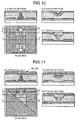
FIG. 10 is a drawing for explaining continuation of the manufacturing method shown in FIG. 9;
FIG. 11 is a drawing for explaining continuation of the manufacturing method shown in FIG. 10;
FIG. 12 is a drawing for explaining continuation of the manufacturing method shown in FIG. 11;
FIGS. 13A to 13D are drawings of the structure of an optical deflecting device according to a second embodiment of the present invention;
FIGS. 14A and 14B are drawings for explaining an optical deflecting device manufacturing method according to the second embodiment;
FIG. 15 is a drawing for explaining continuation of the manufacturing method shown in FIG. 14B;
FIG. 16 is a drawing for explaining continuation of the manufacturing method shown in FIG. 15;
FIG. 17 is a drawing for explaining continuation of the manufacturing method shown in FIG. 16;
FIG. 18 is a drawing for explaining continuation of the manufacturing method shown in FIG. 17;
FIG. 19 is a drawing for explaining continuation of the manufacturing method shown in FIG. 18;
FIG. 20 is a drawing for explaining continuation of the manufacturing method shown in FIG. 19;
FIG. 21 is a drawing for explaining continuation of the manufacturing method shown in FIG. 20;
FIG. 22 is a drawing for explaining continuation of the manufacturing method shown in FIG. 21;
FIG. 23 is a drawing for explaining continuation of the manufacturing method shown in FIG. 22;
FIGS. 24A to 24D are drawings of the structure of an optical deflecting device according to a third embodiment of the present invention;
FIGS. 25A and 25B are drawings for explaining an optical deflecting device according to the third embodiment;
FIG. 26 is a drawing for explaining continuation of the manufacturing method shown in FIG. 25B;
FIG. 27 is a drawing for explaining continuation of the manufacturing method shown in FIG. 26;
FIG. 28 is a drawing for explaining continuation of the manufacturing method shown in FIG. 27;
FIG. 29 is a drawing for explaining continuation of the manufacturing method shown in FIG. 28;
FIG. 30 is a drawing for explaining continuation of the manufacturing method shown in FIG. 29;
FIG. 31 is a drawing for explaining continuation of the manufacturing method shown in FIG. 30;
FIG. 32 is a drawing for explaining continuation of the manufacturing method shown in FIG. 31;
FIG. 33 is a drawing for explaining continuation of the manufacturing method shown in FIG. 32;
FIG. 34 is a drawing for explaining continuation of the manufacturing method shown in FIG. 33; and
FIG. 35 is a schematic drawing of an optical projecting device according to a fourth embodiment of the present invention.
DETAILED DESCRIPTION OF THE PREFERRED EMBODIMENTS
Exemplary embodiments of the present invention are explained below. To avoid redundancy of explanation, in the drawings referred to in the following explanation, same portion or corresponding portions are provided with the same reference numerals.
FIGS. 1A to 1D and 2 are drawings of the structure of an optical deflecting device according to the present embodiment. FIGS. 3A, 3B, and 4 to 12 are drawings for explaining an optical deflecting device manufacturing method according to the present embodiment.
FIG. 1A is a schematic plan view of the optical deflecting device (a plate-shaped member acting as a movable mirror is omitted). FIG. 1B is an A-B schematic cross-section view. FIG. 1C is a C-D schematic cross-section view. FIG. 1D is a schematic side view. Here, in FIG. 1A, the plate-shaped member acting as a movable mirror is omitted because it covers the entire surface. Also in FIG. 1D, the plate-shaped member is omitted.
The optical deflecting device according to the present embodiment includes a silicon substrate 101. On this silicon substrate 101, an oxide film 102 is formed for insulation, on which a pivot member 105 is formed. Also, a group of electrodes 103 is formed, and is then covered with an insulating film 104, such as an oxide film. A conductive plate-shaped member 106 having a light reflecting area is provided. This plate-shaped member 106 has a structure in which it is rotatably supported like a seesaw, with the apex of the pivot member 105 as a pivot. This plate-shaped member 106 is tilted in a direction depicted in FIG. 1B (first tilting direction) or in a reverse direction (second tilting direction). The tilt angle is an approximately arcsin (arcsine) of a value obtained by dividing the height of the pivot member 105 by the half of the length of the plate-shaped member 106.
The plate-shaped member 106 is formed of two layers, that is, an upper layer and a lower layer. On a lower layer 107, a pair of bearing portions 108 formed in a loop is formed for rotatably supporting the plate-shaped member 106. In the present embodiment, the bearing portions 108 have an arc cross-section. Here, the bearing portions 108 are disposed on an end side not engaging the pivot member 105 of the plate-shaped member 106. As most clearly depicted in FIG. 1D, a pair of regulating members 109 is provided so as to correspond to the pair of bearing portions 108. The regulating members 109 each has a stopper 109 a protruding externally in approximately parallel to the silicon substrate 101. This stopper 109 a has a positional relation as depicted in FIG. 1C in which the stopper 109 a enters the bearing portion 108 from the inside and engages the inner surface of the bearing portion 108. Also, the stopper 109 a has an arc-shaped cross-section, and its radius of curvature is approximately equal to the radius of curvature of the inner surface of the bearing portion 108.
FIG. 2 is a drawing for explaining a rotational supporting scheme of the plate-shaped member 106. As depicted in the drawing, with the contact between the bearing portion 108 and the stopper 109 a and the contact between the plate-shaped member 106 and the pivot member 105, the rotation center of the plate-shaped member 106 is determined. Since the radius of curvature of the inner surface of the bearing portion 108 is approximately equal to the radius of curvature of the stopper 109 a, the plate-shaped member 106 can smoothly rotate with the apex of the pivot member 105 as the rotation center. Movement of the plate-shaped member 106 in a rotation axis direction is regulated by vertical side surfaces of the regulating members 109 facing the side surfaces of the bearing portions 108.
Here, the loop-shaped bearing portions 108 preferably have an arc cross-section as in the present embodiment, but can have a polyhedron cross-section. Also, the lower layer 107 of the plate-shaped member 106 is a conductor, such as metal, but can be an insulator.
With the regulating members 109 and the stoppers 109 a being conductors and their potential being equal to the potential of the pivot member 105, even when the plate-shaped member 106 is separated from the pivot member 105 at the time of rotation, the bearing portions 108 and the stopper 109 a are in contact with each other, thereby making the potential of the plate-shaped member 106 equal to the potential of the pivot member 105. The probability of the plate-shaped member 106 electrically making contact with the pivot member 105 and the stoppers 109 a is higher compared with the probability of the plate-shaped member 106 electrically making contact with only the pivot member 105, thereby allowing more stable operation. By controlling the potential of the pivot member 105, the potential of the plate-shaped member 106 is established. Also, with an electrostatic force from a difference with the potential provided to the group of electrodes 103, the tilting direction of the plate-shaped member 106 can be switched between the first tilting direction and the second tilting direction. Therefore, the direction in which the light beam incident to the plate-shaped member 106 is reflected can be switched. Here, such a mechanism of driving of the plate-shaped member 106 is disclosed in detail in Japanese Patent Application Laid-Open No. 2004-78136, and therefore is not explained further more.
The bearing portions 108 are formed on the lower layer 107 side opposite to the light reflecting surface of the plate-shaped member 106. Therefore, since the upper surface of the plate-shaped member 106 does not have a hole or the like, the entire upper surface of the plate-shaped member 106 can be used as a light reflecting area. Thus, when the optical deflecting devices according to the present embodiment are disposed in a two-dimensional array and a light beam is launched from an external light source, a ration of reflecting the incident light beam is determined by the area of the plate-shaped member 106 of each optical deflecting device and a space area between each of the plate-shaped members 106 of adjacent optical deflecting devices, and can be increased to, for example, approximately 91 percent.
Next, a typical process of manufacturing an optical deflecting device explained above is explained. Here, it is assumed that the size of the plate-shaped member 106 measures 10 micrometers per side and its tilt angle is 10 degrees.
Step a: As depicted in FIG. 3A, on a silicon wafer serving as the silicon substrate 101, an insulating film 102 is formed.
Step b: As depicted in FIG. 3B, an Al film serving as the group of electrodes 103 is formed through spattering so as to have a thickness of 200 nanometers, and is then patterned through photolithography by using an organic resist. Then, etching is performed through Reactive Ion etching (RIE) with Cl2 gas to form electrodes. Through a plasma chemical-vapor deposition (CVD) with mixed gas of SiH4 and N2O, an oxide film, which is a protective insulating film 104, is formed so as to have a thickness of 250 nanometers.
Step c: As depicted in FIG. 4, the protective insulating film 104 is etched through photolithography and RIE with mixed gas of CF4 and H2 to open the insulating film. A tungsten W film is then formed so as to have a thickness of 1 micrometer and, by using a photomask with gradation, the pivot member 105 is formed through photolithography so as to have a height of 0.87 micrometers.
Step d: As depicted in FIG. 5, a novolac photoresist serving as a sacrifice layer 201 is applied, and is then planarized through Chemical Mechanical Polishing (CMP). By using the photomask with gradation, a concave surface 202 is formed from the photoresist so as to have an arc-shaped cross-section. This concave surface 202 serves as a basic pattern of the loop shape of the bearing portions 108 on the lower layer 107 of the plate-shaped member 106. At this time, the gradation of the photomask is set so that the concave surface 202 has a predetermined curvature.
Step e: As depicted in FIG. 6, a metal film 203, such as Al or Al—Ti alloy, for example, serving as the lower layer 107 of the plate-shaped member 106 is formed so as to have a thickness of 100 nanometers, and is then etched through photolithography and RIE with Cl2 gas.
Step f: As depicted in FIG. 7, a photoresist is applied through spraying so as to have a thickness of 200 nanometers (film formation through organic film vapor deposition is also possible). Through plasma CVD with mixed gas of SiH4 and N2O, an Si oxide film is formed so as to have a thickness of 100 nanometers. Through photolithography and RIE with mixed gas of CF4 and H2, the Si oxide film is then opened. Through RIE with O2, the photoresist is then etched.
Step g: As depicted in FIG. 8, through plasma CVD with mixed gas of SiH4 and N2O, an Si oxide film is formed so as to have a thickness of 300 nanometers.
Step h: As depicted in FIG. 9, etching is performed through photolithography and RIE with mixed gas of Cf4 and H2.
Step i: As depicted in FIG. 10, a photoresist is applied, and is then planarized through CMP.
Step j: As depicted in FIG. 11, a metal film 204, such as Al or Al—Ti alloy, for example, serving as the upper layer of the plate-shaped member 106 is formed so as to have a thickness of 100 nanometers, and is then etched through photolithography and RIE with Cl2 gas. In a plan view included in FIG. 11, the plate-shaped member 106 covers the entire surface, and therefore part of device is omitted.
Step k: Isotropic etching is performed with O2 plasma and the sacrifice layer of the novolac photoresist is removed, thereby completing an optical deflecting device. In a plan view included in FIG. 12, the plate-shaped member 106 covers the entire surface, and therefore part of device is omitted.
FIGS. 13A to 13D are drawings of the structure of an optical deflecting device according to the present embodiment. FIGS. 14A, 14B, and 15 to 23 are drawings for explaining an optical deflecting device manufacturing method according to the present embodiment.
FIG. 13A is a schematic plan view of the optical deflecting device (a plate-shaped member acting as a movable mirror is omitted). FIG. 13B is an A-B schematic cross-section view. FIG. 13C is a C-D schematic cross-section view. FIG. 13D is a schematic side view. Here, in FIG. 13A, the plate-shaped member acting as a movable mirror is omitted because it covers the entire surface. Also in FIG. 13D, the plate-shaped member is omitted.
In the optical deflecting device according to the present embodiment, the regulating members 109 and the stoppers 109 a are conductors. Other than that, the second embodiment is similar to the first embodiment.
Next, a typical process of manufacturing an optical deflecting device explained above is explained. Here, it is assumed that the size of the plate-shaped member 106 measures 10 micrometers per side and its tilt angle is 10 degrees.
Step a: As depicted in FIG. 14A, on a silicon wafer serving as the silicon substrate 101, the insulating film 102 is formed.
Step b: As depicted in FIG. 14B, an Al film serving as the group of electrodes 103 is formed through spattering so as to have a thickness of 200 nanometers, and is then patterned through photolithography by using an organic resist. Then, etching is performed through RIE with Cl2 gas to form electrodes. Through a plasma CVD with mixed gas of SiH4 and N2O, an oxide film, which is the protective insulating film 104, is formed so as to have a thickness of 250 nanometers.
Step c: As depicted in FIG. 15, the protective insulating film 104 is etched through photolithography and RIE with mixed gas of CF4 and H2 to open the insulating film. A tungsten W film is then formed so as to have a thickness of 1 micrometer and, by using a photomask with gradation, the pivot member 105 is formed through photolithography so as to have a height of 0.87 micrometers.
Step d: As depicted in FIG. 16, a novolac photoresist serving as the sacrifice layer 201 is applied, and is then planarized through Chemical Mechanical Polishing (CMP). By using the photomask with gradation, the concave surface 202 is formed from the photoresist so as to have an arc-shaped cross-section. This concave surface 202 serves as a basic pattern of the loop shape of the bearing portions 108 formed on the lower layer 107 of the plate-shaped member 106. At this time, the gradation of the photomask is set so that the concave surface 202 has a predetermined curvature.
Step e: As depicted in FIG. 17, the metal film 203, such as Al or Al—Ti alloy, for example, serving as the lower layer 107 of the plate-shaped member 106 is formed so as to have a thickness of 100 nanometers, and is then etched through photolithography and RIE with Cl2 gas.
Step f: As depicted in FIG. 18, a photoresist is applied through spraying so as to have a thickness of 200 nanometers (film formation through organic film vapor deposition is also possible). Through spattering, an Al or Al—Ti alloy film is formed so as to have a thickness of 100 nanometers. Through photolithography and RIE with Cl2, the metal film is then opened. Through RIE with O2, the photoresist is then etched.
Step g: As depicted in FIG. 19, through spattering, an Al or Al—Ti alloy film is formed so as to have a thickness of 300 nanometers.
Step h: As depicted in FIG. 20, etching is performed through photolithography and RIE with Cl2.
Step i: As depicted in FIG. 21, a photoresist is applied, and is then planarized through CMP.
Step j: As depicted in FIG. 22, the metal film 204, such as Al or Al—Ti alloy, for example, serving as the upper layer (light reflecting layer) of the plate-shaped member 106 is formed so as to have a thickness of 100 nanometers, and is then etched through photolithography and RIE with Cl2. In a plan view included in FIG. 22, the plate-shaped member 106 covers the entire surface, and therefore part of device is omitted.
Step k: As depicted in FIG. 23, isotropic etching is performed with O2 plasma and the sacrifice layer of the novolac photoresist is removed, thereby completing an optical deflecting device. In a plan view included in FIG. 23, the plate-shaped member 106 covers the entire surface, and therefore part of device is omitted.
FIGS. 24A to 24D are drawings of the structure of an optical deflecting device according to the present embodiment. FIGS. 25A, 25B, and 26 to 34 are drawings for explaining an optical deflecting device manufacturing method according to the present embodiment.
FIG. 24A is a schematic plan view of the optical deflecting device. FIG. 24B is an A-B schematic cross-section view. FIG. 24C is a C-D schematic cross-section view. FIG. 24D is a schematic side view. Here, in FIG. 24A, the plate-shaped member acting as a movable mirror is omitted because it covers the entire surface. Also in FIG. 24D, the plate-shaped member is omitted.
In the optical deflecting device according to the present embodiment, the lower layer 107 of the plate-shaped member 106 and the bearing portions 108 formed thereon are insulators. Also, as the group of electrodes 103, two electrodes “a” and “b” are formed in the first tilting direction of the plate-shaped member, whilst two electrodes “c” and “d” are formed in the second tilting direction thereof. In a driving scheme, when a voltage is applied between the electrodes “a” and “b” in the first tilting direction, an intermediate potential is induced to the plate-shaped member 106. when the intermediate potential between the electrodes “a” and “b” in the first tilting direction is provided to the electrodes “c” and “d” in the second tilting direction, there is no potential difference between the plate-shaped member 106 and the electrodes “c” and “d” in the second tilting direction, thereby preventing an electrostatic force to act. Therefore, the plate-shaped member 106 is tilted in the first direction. Here, such a induced-type driving scheme is disclosed in detail in Japanese Patent Application Laid-Open No. 2004-78136, and therefore is not explained further more.
Next, a typical process of manufacturing an optical deflecting device explained above is explained. Here, it is assumed that the size of the plate-shaped member 106 measures 10 micrometers per side and its tilt angle is 10 degrees.
Step a: As depicted in FIG. 25A, on a silicon wafer serving as the silicon substrate 101, the insulating film 102 is formed.
Step b: As depicted in FIG. 25B, an Al film serving as the group of electrodes 103 is formed through spattering so as to have a thickness of 200 nanometers, and is then patterned through photolithography by using an organic resist. Then, etching is performed through RIE with Cl2 gas to form electrodes. Since a dielectric voltage can be ensured on the lower layer 107 of the plate-shaped member 106, the protective insulating film 104 of the first and second embodiments can be omitted.
Step c: As depicted in FIG. 26, the insulating film 102 is etched through photolithography and RIE with mixed gas of CF4 and H2 to open the insulating film 102. A polysilicon film is then formed through CVD so as to have a thickness of 1 micrometer and, by using a photomask with gradation, the pivot member 105 is formed through photolithography so as to have a height of 0.87 micrometers.
Step d: As depicted in FIG. 27, a novolac photoresist serving as the sacrifice layer 201 is applied, and is then planarized through Chemical Mechanical Polishing (CMP). By using the photomask with gradation, the concave surface 202 is formed from the photoresist so as to have an arc-shaped cross-section. This concave surface 202 serves as a basic pattern of the loop shape of the bearing portions 108 formed on the lower layer 107 of the plate-shaped member 106. At this time, the gradation of the photomask is set so that the concave surface 202 has a predetermined curvature.
Step e: As depicted in FIG. 28, the metal film 203, such as a SiN (silicon nitride) film, serving as the lower layer 107 of the plate-shaped member 106 is formed through CVD, and is then etched through photolithography and RIE with mixed gas of CHF3 and H2.
Step f: As depicted in FIG. 29, a photoresist is applied through spraying so as to have a thickness of 200 nanometers (film formation through organic film vapor deposition is also possible). Through plasma CVD with mixed gas of SiH4 and N2O, a Si oxide film is formed so as to have a thickness of 100 nanometers. Through photolithography and RIE with CF4 and H2, the Si oxide film is then opened. Through RIE with O2, the photoresist is then etched.
Step g: As depicted in FIG. 30, through plasma CVD with mixed gas of SiH4 and N2O, a Si oxide film is formed so as to have a thickness of 300 nanometers.
Step h: As depicted in FIG. 31, the insulating film is etched through photolithography and RIE with mixed gas of Cf4 and H2.
Step i: As depicted in FIG. 32, a photoresist is applied, and is then planarized through CMP.
Step j: As depicted in FIG. 33, the metal film 204, such as Al or Al—Ti alloy, for example, serving as the upper layer (light reflecting layer) of the plate-shaped member 106 is formed, and is then etched through photolithography and RIE with Cl2. In a plan view included in FIG. 33, the plate-shaped member 106 covers the entire surface, and therefore part of device is omitted.
Step k: As depicted in FIG. 34, isotropic etching is performed with O2 plasma and the sacrifice layer of the novolac photoresist is removed, thereby completing an optical deflecting device. In a plan view included in FIG. 34, the plate-shaped member 106 covers the entire surface, and therefore part of device is omitted.
FIG. 35 depicts the structure of an optical projecting device 800 using the optical deflecting device explained above. In FIG. 35, with light having an angle of divergence emitted from a light source 802, an optical deflecting device 801 (or its two-dimensional array) according to the present invention is radiated through, for example, a rotational color filer 805. Reflected light from a light reflecting surface of a plate-shaped member of the optical deflecting device 801 is projected through projection lenses 803 and 806 forming an optical system together with a light shielding unit 804 onto a projection screen 810 when the plate-shaped member is tilted in the first tilting direction. This is an ON state. However, when the plate-shaped member of the optical deflecting device 801 is tilted in the second tilting direction, reflected light from the light reflecting surface is shielded by the light shielding unit 804 serving as a diaphragm, and cannot be projected onto the projection screen. This is an OFF state.
When the two-dimensional array of the optical deflecting device 801 is used, with this ON or OFF, an image can be formed onto the projection screen 810. The optical deflecting device 801 can be used as an optical switching unit of a display (that is, pixel light and dark display) device. Therefore, excellent light and dark control of pixels (that is, ON/OFF control of the optical switch) can be achieved. Also, stray light (reflected light from an adjacent element occurring at the time of distortion in a reflecting direction) can be suppressed. Furthermore, a high-speed operation can be achieved. Still further, high reliability can be achieved for a long time. Still further, driving can be made with low voltage. Still further, a contrast ratio can be increased.
According to an aspect of the present invention, the plate-shaped member can smoothly rotate with the apex of the pivot member as a pivot. Also, its rotation axis tends not to be shifted, thereby allowing stable rotation of the plate-shaped member. Furthermore, there is no hole or the like one the upper surface (light reflecting surface) of the plate-shaped member. Therefore, the entire upper surface of the plate-shaped member can be used as a light reflecting surface.
According to an aspect of the present invention, the bearing portion and the stopper have an approximately arc-shaped cross-section. Therefore, the bearing portion smoothly slides with respect to the stopper, thereby allowing smooth rotation of the plate-shaped member. In particular, According to an aspect of the present invention, the inner surface of the bearing portion and the lower surface of the stopper engaging the inner surface have an approximately equal radius of curvature. Therefore, friction of the bearing portion with respect to the stopper can be further reduced, thereby allowing more smooth rotation of the flat-plate member.
According to an aspect of the present invention, the lower layer of the plate-shaped member is a conductor. Therefore, when the pivot member is a conductor, the potential of the plate-shaped member can be established with an electrical contact between the pivot member and the plate-shaped member.
According to an aspect of the present invention, the lower layer of the plate-shaped member is an insulator. Therefore, an insulating film for insulating the group of electrodes from the plate-shaped member does not have to be formed. This leads to reduction in cost and optical deflecting apparatus manufacturing procedure.
According to an aspect of the present invention, the bearing portion, the regulating member, and the stopper are conductors. Therefore, with electrical contacts among these, even if the pivot member and the plate-shaped member are electrically separated, the potential of the plate-shaped member can be established.
According to an aspect of the present invention, the radius of curvature of the cross-section of the bearing portion and that of the stopper can be approximately equalized.
According to an aspect of the present invention, excellent light and dark control of pixels through ON/OFF control of the optical deflecting device can be achieved. Also, a high-speed operation can be achieved. Furthermore, high reliability can be achieved for a long time. Still further, driving can be made with low voltage. Still further, a contrast ratio can be increased. Therefore, an optical projecting device capable of high-definition image projection with a high contrast ratio can be achieved.
Although the invention has been described with respect to a specific embodiment for a complete and clear disclosure, the appended claims are not to be thus limited but are to be construed as embodying all modifications and alternative constructions that may occur to one skilled in the art that fairly fall within the basic teaching herein set forth.

Claims (8)

1. An optical deflecting device comprising:
a substrate;
a pivot member formed on the substrate;
a regulating member formed on the substrate;
a plate-shaped member having an upper surface as a light reflecting surface; and
a group of electrodes formed on the substrate, wherein
the plate-shaped member has a loop-shaped bearing portion on a lower surface side,
the regulating member has a stopper protruding in approximately parallel to the substrate and embedded inside the bearing portion,
with an engagement of the lower surface of the plate-shaped member and an apex of the pivot member and an engagement of an inner surface of the bearing portion and a lower surface of the stopper, the plate-shaped member is rotatably supported with the apex of the pivot member as a center, and a position of the plate-shaped member in a rotation axis direction is regulated by a side surface of the regulating member facing a side surface of the bearing portion, and
with an electrostatic force generated between the group of electrodes and the plate-shaped member, the plate-shaped member is rotated with the apex of the pivot member as the center, thereby changing a reflecting direction of a light beam incident to the light reflecting surface of the plate-shaped member.
2. The optical deflecting device according to claim 1, wherein the bearing portion and the stopper have an approximately arc-shaped cross section.
3. The optical deflecting device according to claim 1, wherein the inner surface of the bearing portion and the surface of the stopper engaging the inner surface of the bearing portion have an approximately equal radius of curvature.
4. The optical deflecting device according to claim 1, wherein the plate-shaped member is formed of film-laminated layers, and a lower layer of the layers and the bearing portion are conductors.
5. The optical deflecting device according to claim 1, wherein the plate-shaped member is formed of film-laminated layers, and a lower layer of the layers and the bearing portion are insulators.
6. The optical deflecting device according to claim 4, wherein the regulating member and the stopper are conductors.
7. A method of manufacturing the optical deflecting device according to claim 1, the method comprising:
after planarizing a photoresist serving as a sacrifice layer, forming a concave surface corresponding to the bearing portion through etching process;
next forming a film made of a material serving as the lower layer of the plate-shaped member;
next forming and patterning a sacrifice layer along the concave surface; and
next forming a film serving as the stopper of the regulating member.
8. An optical projecting device comprising:
an optical deflecting device including
a substrate;
a pivot member formed on the substrate;
a regulating member formed on the substrate;
a plate-shaped member having an upper surface as a light reflecting surface; and
a group of electrodes formed on the substrate, wherein
the plate-shaped member has a loop-shaped bearing portion on a lower surface side,
the regulating member has a stopper protruding in approximately parallel to the substrate and embedded inside the bearing portion,
with an engagement of the lower surface of the plate-shaped member and an apex of the pivot member and an engagement of an inner surface of the bearing portion and a lower surface of the stopper, the plate-shaped member is rotatably supported with the apex of the pivot member as a center, and a position of the plate-shaped member in a rotation axis direction is regulated by a side surface of the regulating member facing a side surface of the bearing portion, and
with an electrostatic force generated between the group of electrodes and the plate-shaped member, the plate-shaped member is rotated with the apex of the pivot member as the center, thereby changing a reflecting direction of a light beam incident to the light reflecting surface of the plate-shaped member;
a light source that light up a light reflecting surface of a plate-shaped member of the optical deflecting device; and
an optical system that projects light reflected from the light reflecting surface when the plate-shaped member of the optical deflecting device is tilted in a first tilting direction, and shields light reflected from the light reflecting surface and prevents the light from being projected outside when the plate-shaped member is tilted in a second tilting direction.
US11/681,021 2006-03-01 2007-03-01 Optical deflecting device, optical deflecting device manufacturing method, and optical projecting device Expired - Fee Related US7277217B1 (en)

Applications Claiming Priority (2)

Application Number Priority Date Filing Date Title
JP2006-055050 2006-03-01
JP2006055050A JP2007233065A (en) 2006-03-01 2006-03-01 Light deflector, manufacturing method therefor, and optical projector

Publications (2)

Publication Number Publication Date
US20070206268A1 US20070206268A1 (en) 2007-09-06
US7277217B1 true US7277217B1 (en) 2007-10-02

Family

ID=38471211

Family Applications (1)

Application Number Title Priority Date Filing Date
US11/681,021 Expired - Fee Related US7277217B1 (en) 2006-03-01 2007-03-01 Optical deflecting device, optical deflecting device manufacturing method, and optical projecting device

Country Status (2)

Country Link
US (1) US7277217B1 (en)
JP (1) JP2007233065A (en)

Cited By (2)

* Cited by examiner, † Cited by third party
Publication number Priority date Publication date Assignee Title
US20080117488A1 (en) * 2001-11-14 2008-05-22 Takeshi Nanjyo Light deflecting method and apparatus efficiently using a floating mirror
US20080225367A1 (en) * 2007-03-15 2008-09-18 Seiichi Katoh Optical deflecting device

Families Citing this family (4)

* Cited by examiner, † Cited by third party
Publication number Priority date Publication date Assignee Title
JP5527152B2 (en) * 2010-10-07 2014-06-18 株式会社豊田中央研究所 Optical deflection device
WO2014080444A1 (en) * 2012-11-26 2014-05-30 パイオニア株式会社 Electrostatic actuator and variable capacitance device
JP6600480B2 (en) * 2015-04-20 2019-10-30 東京エレクトロン株式会社 Method for processing an object
DE102017205047B4 (en) * 2017-03-24 2022-02-17 Fraunhofer-Gesellschaft zur Förderung der angewandten Forschung e.V. Micromechanical actuator device and method for its manufacture

Citations (24)

* Cited by examiner, † Cited by third party
Publication number Priority date Publication date Assignee Title
JP2002525676A (en) 1998-09-24 2002-08-13 リフレクティヴィティー, インク. Double-substrate reflective spatial light modulator with self-control micromechanical elements
US20020181069A1 (en) * 2001-03-30 2002-12-05 Gsi Lumonics Corporation Free space optical switch
US6522452B2 (en) * 2001-04-26 2003-02-18 Jds Uniphase Corporation Latchable microelectromechanical structures using non-newtonian fluids, and methods of operating same
JP3411014B2 (en) 2000-11-02 2003-05-26 株式会社東芝 Inductive charge mirror
US6628447B1 (en) * 1999-12-06 2003-09-30 Xerox Corporation Array of rotatable solid elements for color display
JP3492400B2 (en) 1992-10-15 2004-02-03 テキサス インスツルメンツ インコーポレイテツド Bi-stable DMD addressing method
US6700688B2 (en) * 2001-08-24 2004-03-02 Megasense, Inc. Rolling mirror apparatus and method of use
JP2004078136A (en) 2001-11-14 2004-03-11 Ricoh Co Ltd Optical deflection method and device, method for manufacturing optical deflecting device, optical information processor provided with the optical deflecting device, image forming device image projecting and display device and optical transmitting device
JP2004138881A (en) 2002-10-18 2004-05-13 Ricoh Co Ltd Picture projection display device
US6738177B1 (en) * 2000-09-05 2004-05-18 Siwave, Inc. Soft snap-down optical element using kinematic supports
US20040150872A1 (en) * 1999-11-16 2004-08-05 Xros, Inc., A California Corporation Two-dimensional micro-mirror array enhancements
US6900915B2 (en) 2001-11-14 2005-05-31 Ricoh Company, Ltd. Light deflecting method and apparatus efficiently using a floating mirror
JP2005195798A (en) 2004-01-06 2005-07-21 Ricoh Co Ltd Light deflector
US6947195B2 (en) 2001-01-18 2005-09-20 Ricoh Company, Ltd. Optical modulator, optical modulator manufacturing method, light information processing apparatus including optical modulator, image formation apparatus including optical modulator, and image projection and display apparatus including optical modulator
US20050248862A1 (en) 2004-04-05 2005-11-10 Takeshi Nanjo Light deflector, light deflection array, image forming apparatus, and image projection display apparatus
US7042621B2 (en) * 2004-01-20 2006-05-09 Pentax Corporation Micromirror device
US20060104597A1 (en) 2004-10-20 2006-05-18 Takeshi Nanjo Optical system, color information displaying method, optical deflecting device, and image projection displaying apparatus
US20060103912A1 (en) 2004-10-21 2006-05-18 Seiichi Katoh Optical deflection device and image projection display apparatus using the same
US7050217B2 (en) 2003-06-27 2006-05-23 Ricoh Company, Ltd. Method for driving light deflector, light deflector, light deflection array, image forming device, and image projection display apparatus
JP2006133394A (en) 2004-11-04 2006-05-25 Ricoh Co Ltd Method of driving optical deflection apparatus array, optical deflection apparatus array, optical deflection apparatus, and picture projection display apparatus
US7075562B2 (en) 2002-07-17 2006-07-11 Ricoh Company, Ltd. Optical scanning device
US20060198007A1 (en) * 2005-03-02 2006-09-07 Texas Instruments Incorporated Method of adjusting the resonant frequency of an assembled torsional hinged device
US7113321B2 (en) 2003-04-15 2006-09-26 Ricoh Company, Ltd. Optical deflection apparatus and manufacturing method thereof, optical deflection array, imaging apparatus, and image projection display apparatus
US20060239009A1 (en) 2005-04-20 2006-10-26 Takeshi Nanjyo Light deflector, light deflection array, optical system, image forming device, and projection type image display apparatus

Patent Citations (31)

* Cited by examiner, † Cited by third party
Publication number Priority date Publication date Assignee Title
JP3492400B2 (en) 1992-10-15 2004-02-03 テキサス インスツルメンツ インコーポレイテツド Bi-stable DMD addressing method
JP2002525676A (en) 1998-09-24 2002-08-13 リフレクティヴィティー, インク. Double-substrate reflective spatial light modulator with self-control micromechanical elements
US20040150872A1 (en) * 1999-11-16 2004-08-05 Xros, Inc., A California Corporation Two-dimensional micro-mirror array enhancements
US6628447B1 (en) * 1999-12-06 2003-09-30 Xerox Corporation Array of rotatable solid elements for color display
US6738177B1 (en) * 2000-09-05 2004-05-18 Siwave, Inc. Soft snap-down optical element using kinematic supports
JP3411014B2 (en) 2000-11-02 2003-05-26 株式会社東芝 Inductive charge mirror
US6947195B2 (en) 2001-01-18 2005-09-20 Ricoh Company, Ltd. Optical modulator, optical modulator manufacturing method, light information processing apparatus including optical modulator, image formation apparatus including optical modulator, and image projection and display apparatus including optical modulator
US7166486B2 (en) 2001-01-18 2007-01-23 Ricoh Company, Ltd. Optical modulator, optical modulator manufacturing method, light information processing apparatus including optical modulator, image formation apparatus including optical modulator, and image projection and display apparatus including optical modulator
US20020181069A1 (en) * 2001-03-30 2002-12-05 Gsi Lumonics Corporation Free space optical switch
US6522452B2 (en) * 2001-04-26 2003-02-18 Jds Uniphase Corporation Latchable microelectromechanical structures using non-newtonian fluids, and methods of operating same
US6700688B2 (en) * 2001-08-24 2004-03-02 Megasense, Inc. Rolling mirror apparatus and method of use
US7064878B2 (en) 2001-11-14 2006-06-20 Ricoh Company, Ltd. Light deflecting method and apparatus efficiently using a floating mirror
JP2004078136A (en) 2001-11-14 2004-03-11 Ricoh Co Ltd Optical deflection method and device, method for manufacturing optical deflecting device, optical information processor provided with the optical deflecting device, image forming device image projecting and display device and optical transmitting device
US6900915B2 (en) 2001-11-14 2005-05-31 Ricoh Company, Ltd. Light deflecting method and apparatus efficiently using a floating mirror
US20060187514A1 (en) 2001-11-14 2006-08-24 Takeshi Nanjyo Light deflecting method and apparatus efficiently using a floating mirror
US7099060B2 (en) * 2001-11-14 2006-08-29 Ricoh Company, Ltd. Light deflecting method and apparatus efficiently using a floating mirror
US7075562B2 (en) 2002-07-17 2006-07-11 Ricoh Company, Ltd. Optical scanning device
JP2004138881A (en) 2002-10-18 2004-05-13 Ricoh Co Ltd Picture projection display device
US7113321B2 (en) 2003-04-15 2006-09-26 Ricoh Company, Ltd. Optical deflection apparatus and manufacturing method thereof, optical deflection array, imaging apparatus, and image projection display apparatus
US7050217B2 (en) 2003-06-27 2006-05-23 Ricoh Company, Ltd. Method for driving light deflector, light deflector, light deflection array, image forming device, and image projection display apparatus
US20060171015A1 (en) 2003-06-27 2006-08-03 Takeshi Nanjyo Method for driving light deflector, light deflector, light deflection array, image forming device, and image projection display apparatus
US7167290B2 (en) 2004-01-06 2007-01-23 Ricoh Company, Ltd. Optical deflection device
JP2005195798A (en) 2004-01-06 2005-07-21 Ricoh Co Ltd Light deflector
US7042621B2 (en) * 2004-01-20 2006-05-09 Pentax Corporation Micromirror device
US20050248862A1 (en) 2004-04-05 2005-11-10 Takeshi Nanjo Light deflector, light deflection array, image forming apparatus, and image projection display apparatus
US20060104597A1 (en) 2004-10-20 2006-05-18 Takeshi Nanjo Optical system, color information displaying method, optical deflecting device, and image projection displaying apparatus
US20060103912A1 (en) 2004-10-21 2006-05-18 Seiichi Katoh Optical deflection device and image projection display apparatus using the same
US20060109539A1 (en) 2004-11-04 2006-05-25 Seiichi Katoh Method for driving optical deflecting device array, optical deflecting device array, optical deflecting device, and image projection displaying apparatus
JP2006133394A (en) 2004-11-04 2006-05-25 Ricoh Co Ltd Method of driving optical deflection apparatus array, optical deflection apparatus array, optical deflection apparatus, and picture projection display apparatus
US20060198007A1 (en) * 2005-03-02 2006-09-07 Texas Instruments Incorporated Method of adjusting the resonant frequency of an assembled torsional hinged device
US20060239009A1 (en) 2005-04-20 2006-10-26 Takeshi Nanjyo Light deflector, light deflection array, optical system, image forming device, and projection type image display apparatus

Non-Patent Citations (3)

* Cited by examiner, † Cited by third party
Title
Chang-Hyeon Ji, et al., "Design, Fabrication, and Experiment of Micromirror with Aluminum Pin-Joints", Micro Opto Electro Mechanical Systems-MOEMS, 1999, pp. 44-48.
Larry J. Hornbeck, "Deformable-Mirror Spatial Light Modulators", SPIE Critical Reviews Series, vol. 1150, 1989, pp. 86-102.
Peter F. Van Kessel, et al., "A MEMS-Based Projection Display", Proceedings of the IEEE, vol. 86, No. 8, Aug. 1998, pp. 1687-1704.

Cited By (4)

* Cited by examiner, † Cited by third party
Publication number Priority date Publication date Assignee Title
US20080117488A1 (en) * 2001-11-14 2008-05-22 Takeshi Nanjyo Light deflecting method and apparatus efficiently using a floating mirror
US7457019B2 (en) 2001-11-14 2008-11-25 Ricoh Company, Ltd. Light deflecting method and apparatus efficiently using a floating mirror
US20080225367A1 (en) * 2007-03-15 2008-09-18 Seiichi Katoh Optical deflecting device
US7965431B2 (en) 2007-03-15 2011-06-21 Ricoh Company, Ltd. Optical deflecting device

Also Published As

Publication number Publication date
JP2007233065A (en) 2007-09-13
US20070206268A1 (en) 2007-09-06

Similar Documents

Publication Publication Date Title
JP3889705B2 (en) Micromirror device, package for micromirror device, and projection system therefor
US7277217B1 (en) Optical deflecting device, optical deflecting device manufacturing method, and optical projecting device
US6867897B2 (en) Micromirrors and off-diagonal hinge structures for micromirror arrays in projection displays
US7075702B2 (en) Micromirror and post arrangements on substrates
US6974713B2 (en) Micromirrors with mechanisms for enhancing coupling of the micromirrors with electrostatic fields
US20060285193A1 (en) Optical modulation element array
US20030214639A1 (en) Micromirrors with OFF-angle electrodes and stops
US8199394B2 (en) Mircromirror device having a vertical hinge
US7933060B2 (en) Three states of micro mirror device
US7265892B2 (en) Micromirror array devices with light blocking areas
US7167290B2 (en) Optical deflection device
US7436572B2 (en) Micromirrors and hinge structures for micromirror arrays in projection displays
US7760415B2 (en) Micro mirror device
US7876488B2 (en) Mirror device having vertical hinge
JP2005292684A (en) Optical deflection apparatus, optical deflection array, image forming apparatus and image projection apparatus
US7755830B2 (en) Micro mirror device
JP2007199096A (en) Light deflector and light deflector array
JP4544574B2 (en) Optical deflection device
US20060050353A1 (en) Micromirrors and hinge structures for micromirror arrays in projection displays
US7633665B2 (en) Optical modulator element and image forming apparatus
US7362495B2 (en) Electrostatic fins for a MEMS device

Legal Events

Date Code Title Description
AS Assignment

Owner name: RICOH COMPANY, LTD., JAPAN

Free format text: ASSIGNMENT OF ASSIGNORS INTEREST;ASSIGNORS:KATOH, SEIICHI;NANJYO, TAKESHI;OHTAKA, KOICHI;REEL/FRAME:018948/0711

Effective date: 20070221

FEPP Fee payment procedure

Free format text: PAYOR NUMBER ASSIGNED (ORIGINAL EVENT CODE: ASPN); ENTITY STATUS OF PATENT OWNER: LARGE ENTITY

CC Certificate of correction
FEPP Fee payment procedure

Free format text: PAYER NUMBER DE-ASSIGNED (ORIGINAL EVENT CODE: RMPN); ENTITY STATUS OF PATENT OWNER: LARGE ENTITY

Free format text: PAYOR NUMBER ASSIGNED (ORIGINAL EVENT CODE: ASPN); ENTITY STATUS OF PATENT OWNER: LARGE ENTITY

REMI Maintenance fee reminder mailed
LAPS Lapse for failure to pay maintenance fees
STCH Information on status: patent discontinuation

Free format text: PATENT EXPIRED DUE TO NONPAYMENT OF MAINTENANCE FEES UNDER 37 CFR 1.362

FP Lapsed due to failure to pay maintenance fee

Effective date: 20111002