US7228076B2 - Method for remodulation of a modulated optical signal and device for remodulation and transmission system - Google Patents
Method for remodulation of a modulated optical signal and device for remodulation and transmission system Download PDFInfo
- Publication number
- US7228076B2 US7228076B2 US10/373,023 US37302303A US7228076B2 US 7228076 B2 US7228076 B2 US 7228076B2 US 37302303 A US37302303 A US 37302303A US 7228076 B2 US7228076 B2 US 7228076B2
- Authority
- US
- United States
- Prior art keywords
- signal
- raman
- optical
- raman pump
- disturbed
- Prior art date
- Legal status (The legal status is an assumption and is not a legal conclusion. Google has not performed a legal analysis and makes no representation as to the accuracy of the status listed.)
- Active, expires
Links
Images


Classifications
-
- H—ELECTRICITY
- H04—ELECTRIC COMMUNICATION TECHNIQUE
- H04B—TRANSMISSION
- H04B10/00—Transmission systems employing electromagnetic waves other than radio-waves, e.g. infrared, visible or ultraviolet light, or employing corpuscular radiation, e.g. quantum communication
- H04B10/29—Repeaters
- H04B10/291—Repeaters in which processing or amplification is carried out without conversion of the main signal from optical form
- H04B10/299—Signal waveform processing, e.g. reshaping or retiming
-
- H—ELECTRICITY
- H04—ELECTRIC COMMUNICATION TECHNIQUE
- H04B—TRANSMISSION
- H04B10/00—Transmission systems employing electromagnetic waves other than radio-waves, e.g. infrared, visible or ultraviolet light, or employing corpuscular radiation, e.g. quantum communication
- H04B10/25—Arrangements specific to fibre transmission
- H04B10/2507—Arrangements specific to fibre transmission for the reduction or elimination of distortion or dispersion
- H04B10/2543—Arrangements specific to fibre transmission for the reduction or elimination of distortion or dispersion due to fibre non-linearities, e.g. Kerr effect
- H04B10/2557—Cross-phase modulation [XPM]
-
- H—ELECTRICITY
- H04—ELECTRIC COMMUNICATION TECHNIQUE
- H04B—TRANSMISSION
- H04B10/00—Transmission systems employing electromagnetic waves other than radio-waves, e.g. infrared, visible or ultraviolet light, or employing corpuscular radiation, e.g. quantum communication
- H04B10/29—Repeaters
- H04B10/291—Repeaters in which processing or amplification is carried out without conversion of the main signal from optical form
- H04B10/2912—Repeaters in which processing or amplification is carried out without conversion of the main signal from optical form characterised by the medium used for amplification or processing
- H04B10/2916—Repeaters in which processing or amplification is carried out without conversion of the main signal from optical form characterised by the medium used for amplification or processing using Raman or Brillouin amplifiers
Definitions
- the invention deals with a method for remodulation of a modulated optical signal using a disturbed line signal and an optical clock signal derived from the undisturbed original line signal modulated with the bitrate frequency, feeding both signals in a Raman amplifying fiber connected to at least one Raman pump and running the clock signal as Raman pump wavelength for the line signal.
- the invention is also related to a device for remodulation of optical signals with an input for line signals and a coupler, the coupler connects the line and a Raman pump laser with a piece of Raman active fiber, and the Ramon pump laser is connected to a clock recovery device which modulates the Raman pump laser light with the bit rate frequency of the optical signal.
- the invention is also related to a transmission system for transmission of optical signals in transmission lines comprising transmitter means, receiver means and regeneration means in the line where the regeneration means have devices to recover amplitude, clock and shape of the signals, the clock recovery device comprises means to recover an optical clock signal, the said optical clock signals is connected to a remodulation device as described in the invention.
- Optical communication systems are a fast-growing constituent of communication networks.
- the term “optical communication system” as used in the following relates to any system or device which makes use of optical signals to transport information across an optical waveguiding medium.
- Optical communication systems comprise inter alia telecommunication systems, local area networks (LAN), cable television systems etc.
- Optical communications at ultra-high bit-rates with bit rates for example over 40 Gbit/s over long distance suffers from severe degradations occurring during propagation.
- optical signal recovery is one of the core technologies involved in this process.
- a key to this evolution is the availability of extremely-broad-band optical devices, offering modulation, regeneration, amplification over nearly all the transmission window allowed by silica.
- optical regeneration by synchronous modulation was proven to alleviate limitations of transmission due to reduction of timing litter, decreasing polarisation mode dispersion impact, improvement of optical signal-to noise ratio at low bit error rate levels.
- Electro-optical interferometers are well known. But this InP or LiNbO 3 MZ devices, suffer from rather high insertion loss (>10 dB for InP, >8 dB for PI-concatenated LiNbO 3 ), which in turn limits or even suppresses the benefit of synchronous optical regeneration. They also face a problem from the operating speed limit imposed by electronic circuitries and electrode phase-matching which is typical 40 GHz. Their power consumption is rather high (>10 W), which limits their interest for submarine-cable applications. Finally, their optical power-handling capability is limited ( ⁇ 100 mW), which prevents massive/simultaneous WDM optical regeneration.
- the EP 0 975 106 discloses a system where a digital modulation is extracted for regeneration using an optical coupler and clock extractor, and semiconductor amplifiers are used in an amplitude or phase modulator arrangement to modulate soliton pulses.
- the device comprises an optical coupler and electro-optical recovery unit for recovery of the clock signal from the incoming signal in the input line (F 1 ). This permits the extraction of digital information for regenerating use and a means of modulation of the amplitude and/or the phase of the solitons by the clock signal.
- the device is characterized by the use of a Mach-Zehnder modulator containing first and second optical semiconductor amplifiers arranged in two parallel arms with the gain of each modulated by the recovered clock signal.
- the output signals from the recovery unit are fed to a splitting circuit providing, through delay circuits feedback to amplifiers in the modulator.
- the output line contains the-signal of same wavelength as the input line, with the clock signals blocked by the feedback signals.
- Optical fibre Raman amplifiers are well known and are known to be designed to operate at a desired wavelengths between 1.25 ⁇ m and 1.7 ⁇ m.
- FRA utilize silica-based fibres and display a high transparency when unpumped.
- the working principle of FRA is based on stimulated Raman scattering FRA can serve for example as a replacement for conventional repeaters or semiconductor-amplifiers, or for rare-earth-doped fibre amplifiers or in combination with them.
- a Raman amplifier uses stimulated Raman scattering, which occurs in silica fibers when an intense pump beam propagates through it.
- Stimulated Raman scattering is an inelastic scattering process in which an incident pump photon looses its energy to create another photon of reduced energy at a lower frequency. The remaining energy is absorbed by the fiber medium in the form of molecular vibrations (i.e., optical phonons). That is, pump energy of a given wavelength amplifies a signal at a longer wavelength. This process is named a Stokes scattering.
- an incident pump photon absorbs the energy of a molecular vibration and a photon with a higher energy than the incident photon is emitted. This process is a Anti-Stokes scattering.
- Roman amplifiers offer a number of advantages over rare-earth doped amplifiers. For example, they are relatively low noise devices with a gain spectrum that is very broad in comparison to rare-earth doped amplifiers.
- Raman amplifiers can achieve up to 100 nm without bandsplitting.
- Raman amplifiers can be used for distributed amplification. That is, the same fiber that is used for signal transmission is also used for signal amplification.
- rare-earth doped optical amplifiers typically used only provide lumped amplification in which gain is imparted only in a particular section of fiber that contains an appropriate dopant.
- Raman amplifiers may also be used to provide lumped amplification.
- Raman amplifiers do not rely on the presence of a special amplifier fiber since the gain medium can be the transmission fiber itself.
- This experimental setup does not work with the clock signal of a real transmitted signal and does not comprise a mean for extracting the clock signal.
- the invention solve the problems of the modulation devices by using a method for remodulation of a high frequency modulated optical signals using a disturbed line signal and an optical clock signal derived from the undisturbed original line signal modulated with the bitrate frequency, feeding both signals in a Raman amplifying fiber connected to at least one Raman pump and running the clock signal as Roman pump wavelength for the line signal.
- the advantage of the proposed method for remodulation of optical signals with a Roman modulator is that the modulation signal, the clock signal is in one step derived from the disturbed signal itself.
- the use of an optical clock recovery signal avoids problems with electronic high frequency modulators.
- the use of the method of the invention allows a simple adjustment of the modulation depth of the Raman signal by adapting the spectral position of the Raman pump in relation to the signal. This phase modulation dept can also be influenced by the pump power of the Raman pump.
- Using at least two Raman pumps that are coupled in phase can avoid problem with by cross phase modulation.
- the method to couple the at least two Raman pump wavelengths out of phase allows the pure intensity modulation free of phase effects.
- the invention also proposes a device for remodulating of an optical signal with an input for line signals in a coupler.
- the coupler connects the line in a Raman pump laser with a piece of Raman active fiber and the Raman pump laser is connected to clock recovery device which modulates the Raman pump laser light with a bit rate frequency of the optical signal.
- This device has a layout without a RF modulator based on an electronic device.
- the signal is derived from a clock recovery device, which is an optical signal. This extracted optical clock signal is directly launched into the Raman pump.
- the Raman pump wavelength is selected as a shorter or a longer wavelength than the signal wavelength itself.
- Another preferred embodiment of the device for optical remodulation comprises at least two Raman pumps.
- the advantage of the second configuration is the relaxed constrains on the modulated Raman pump. Only a very limited power is sufficient to generate a strong signal modulation because of the internal Raman gain experience by this pump.
- Another preferred embodiment of the device for optical remodulation uses two Roman pumps, which are modulated simultaneously with the clock recovery signal. This device avoids parasitic phase effects on the modulation. A pure phase or a pure intensity modulation is obtained.
- a transmission system using the devices of the invention and an optical clock recovery signal for driving the device for remodulation of optical signals has the advantage to reduce the power consumption of the regeneration means.
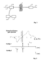
- FIG. 1 shows a first embodiment of the invention
- FIG. 2 a schematic wavelength scheme of the first embodiment
- FIG. 3 a second embodiment of the invention
- FIG. 4 a wavelength scheme for the second embodiment
- FIG. 5 the gain spectrum and phase responds of the device
- FIG. 6 a third embodiment of the invention
- FIG. 7 a symmetric Raman arrangement spectrum.
- FIG. 1 describes a first embodiment of the invention.
- the transmission line 4 is connected to a first coupler 3 a . Via the line 4 a line disturbed signal 1 is fed into the coupler 3 a .
- the second input of the coupler 3 a is connected to a Raman pump 6 A.
- the Raman pump 6 A is connected to a clock recovery device 7 .
- the output of the coupler 3 a is connected to Raman fiber piece 5 .
- the output of the Raman fiber piece 5 is than connected again to the line 4 via a filter 8 .
- the disturbed signal 1 carries the clock signal and the bit information in form of modulation of intensity of light. For several effect of the transmission line the signal is disturbed and the intensity of the modulation decreased.
- the Raman pump provides a periodic clock signal, which is derived from a clock recovery system, which recovers the bit rate frequency in an electronic way.
- a clock recovery circuit is described in EP 0 975 106.
- the resulting RF signal is converted to an optical signal using a standard low power gain switched DFB laser.
- the clock signal is derived optically from the line signal.
- a device for regenerating optical signals by amplitude and phase modulation of the optical signals comprising: a mode locked laser enabling a clock signal to be recovered representative of the clock rate of the bits in the optical signals to be regenerated; and a modulating interferometer structure having first and second interferometer arms and enabling the amplitude and the phase of the optical signals to be modulated by said clock signal, and including at least one semiconductor optical amplifier disposed in the first interferometer arm.
- the mode locked laser is coupled to said first interferometer arm in such a manner that said amplifier of the first interferometer arm is a component that is common both to the mode locked laser and to said interferometer structure.
- optical signals from the optical clock recovery device can be coupled directly into the second port of the coupler 3 A.
- This periodic Raman pump signal is fed into the Raman amplifying fiber 5 in phase with the disturbed line signal 1 .
- the Raman amplifying fiber 5 should be a fiber with a high Raman efficiency as for example the holy fiber of the prior art document.
- the invention is also realized using conventional available fiber without special high efficiency for Raman amplification.
- two configurations are possible as shown in FIG. 2 .
- FIG. 2 shows in the above spectrum the normalised Raman gain spectrum, which shows the efficiency verses the difference between pump wavelength and the signal wavelength.
- the Raman pump wavelength is shorter than the signal wavelength.
- the energy transfer from the pump wavelength to the signal wavelength is following a Stoke process.
- the pump wavelength is longer than the signal wavelength.
- the energy transfer is done in Anti-Stoke process.
- the Raman amplification takes place when the modulated Raman pump signal is in phase with the disturbed line signal. When the Raman pump signal is zero no amplification takes place and the disturbed signals or noise signals are suppressed. What can also derive from the normalised Raman spectrum is that the device works also in a wavelength multiplex and the Raman amplification can simultaneous regenerated a WDM wavelength comb when the WDM channels are resynchronised prior to the remodulation.
- the Raman pump process is realized in a co-propagation with the signals.
- a counter-propagation remodultion device is realized where the Raman pump signal is fed into the Raman amplifying fiber with a coupler arranged after the Raman amplifying fiber piece in direction of the signal.
- FIG. 3 shows a second embodiment of the invention. Additionally to the configuration of FIG. 1 a second coupler 3 B between the first coupler 3 A and the amplifying fiber piece 5 is arranged. This second coupler 3 B is connected to a second Raman pump 6 B. In this arrangement the modulated pump 6 A itself is amplified by the second Raman pump 6 B with a continuous wave signal. The weak signal from the optical clock recovery is directly lounged into the fiber to act as a modulated pump. The modulated signal is boosted by Raman amplification by the Raman pump 6 B.
- FIG. 4 shows the wavelength scheme for the configuration of the device described in FIG. 3 .
- the strong continuous-wave pump 6 B pumps in the first step with ⁇ (pump 6 B) the modulated Raman pump 6 A and the Raman pump 6 A with ⁇ (pump 6 A) in a second step the wavelength ⁇ (signal) of the signal.
- ⁇ signal
- the arrangement of FIG. 3 shows a copropagating Raman pumping scheme. This is only an example for the inventional solution. Also counter propagating or bi-directional pumping is used to obtain the result of the inventional method.
- the clock recovery device 7 is not explained in details. The clock recovery can be done in several ways all-optical or in electro-optical recovery unit. The connection of the optical clock recovery device 7 to the optical transmission line is not shown in the figure.
- FIG. 6 shows the third preferred embodiment of the invention.
- the first coupler 3 A is connected to a first Raman pump 6 A and a clock recovery device 7 A.
- the output of the first coupler 3 a is via the Raman amplifying fiber piece 5 connected to a second coupler 3 B.
- the second input of this coupler 3 B is connected to a second Raman pump 6 B which is also connected to a clock recovers device 7 B.
- the clock recovery devices 7 A and 7 B which are shown as two building blocks in the figure are realized as one device which couples the optical signals.
- the first Raman pump pumps the signal with a lower wavelength and the second Raman pump pumps the signal with higher wavelength.
- the two wavelengths are symmetrically arranged around the signal wavelength.
- Raman modulates phase the problem of a phase modulation induced by cross phase modulation effect between modulated pump signal and line signal.
- High speed signal processing applications require non linear device response in the ns/ps time scale. Such non linear responses can be generated in standard silica fibers through the optical Kerr effect, which causes self and cross-phase modulation. As these effect are based on third order non linear interactions with very weak susceptibilities the optical power required to observe them are relatively high.
- the Raman modulation effect can be described by equation (1) where the modulated pumps P has a periodic signal, C describes the Raman efficiency coefficient of the fiber at the pump wavelength and L is effected length of each pump:
- ⁇ ⁇ ⁇ P dB ⁇ ( t ) 10 ln ⁇ ( 10 ) ⁇ m ⁇ [ C R1 ⁇ P 1 ⁇ L eff1 ⁇ cos ⁇ ( 2 ⁇ ⁇ ⁇ ⁇ f ⁇ ⁇ t ) - C R2 ⁇ P 2 ⁇ L eff2 ⁇ cos ⁇ ( 2 ⁇ ⁇ ft + ⁇ ) ] ( 1 )
- ⁇ ⁇ ⁇ P dB ⁇ ( t ) 10 ln ⁇ ( 10 ) ⁇ mP 1 ⁇ L eff1 ⁇ ( C R1 + C R2 ) ⁇ cos ⁇ ( 2 ⁇ ⁇ ⁇ ⁇ f ⁇ ⁇ t + ⁇ )
- phase modulation is:
- ⁇ ⁇ ( t ) 4 ⁇ ⁇ ⁇ ⁇ n 2 A eff ⁇ mP 1 ⁇ L eff1 ⁇ ( 1 + C R1 C R2 ) ⁇ cos ⁇ ( 2 ⁇ ⁇ ⁇ ⁇ ft )
- the modulation transfer at high bit rates requires very low chromatic dispersion between pump and signal.
- the chromatic dispersion between the two pumps must also be very low.
- the Raman fiber should be enable the same group velocity for the three implied wavelength.
- the basic configuration of FIG. 6 includes also devices with more then the two Roman pumps. All kind of cascading Raman schemes working with symmetric Raman pumps are able to realize the method for remodulating a signal via a coupling of the different Raman pumps.
Landscapes
- Physics & Mathematics (AREA)
- Electromagnetism (AREA)
- Engineering & Computer Science (AREA)
- Computer Networks & Wireless Communication (AREA)
- Signal Processing (AREA)
- Nonlinear Science (AREA)
- Optical Modulation, Optical Deflection, Nonlinear Optics, Optical Demodulation, Optical Logic Elements (AREA)
- Optical Communication System (AREA)
- Lasers (AREA)
- Optical Couplings Of Light Guides (AREA)
Abstract
Description
- CRi: Raman efficiency coefficient of the fiber at each pump wavelength
- Leffi: Effective length of each pump
Raman Modulation Effect
coupling the two modulated pumps with the same intensity and a phase shift of φ=π the resulting cross phase modulation is zero, see relation 3.
→ Chirp-Free Intensity Modulation: (ref 1)
P 1 L eff1 =P 2 L eff2
and
φ=π
so that
ΔΦ(t)=0 (chirp free) (3)
C R1 P 1 L eff1 =C R2 P 2 L eff2
and
φ=0
so that
ΔP dB(t)=0 (constant intensity) (4)
Claims (10)
Applications Claiming Priority (2)
| Application Number | Priority Date | Filing Date | Title |
|---|---|---|---|
| EP02360129.7 | 2002-04-24 | ||
| EP02360129A EP1357686B1 (en) | 2002-04-24 | 2002-04-24 | Remodulator for optical communication systems |
Publications (2)
| Publication Number | Publication Date |
|---|---|
| US20030202797A1 US20030202797A1 (en) | 2003-10-30 |
| US7228076B2 true US7228076B2 (en) | 2007-06-05 |
Family
ID=28686026
Family Applications (1)
| Application Number | Title | Priority Date | Filing Date |
|---|---|---|---|
| US10/373,023 Active 2025-03-15 US7228076B2 (en) | 2002-04-24 | 2003-02-26 | Method for remodulation of a modulated optical signal and device for remodulation and transmission system |
Country Status (4)
| Country | Link |
|---|---|
| US (1) | US7228076B2 (en) |
| EP (1) | EP1357686B1 (en) |
| AT (1) | ATE387043T1 (en) |
| DE (1) | DE60225116T2 (en) |
Families Citing this family (4)
| Publication number | Priority date | Publication date | Assignee | Title |
|---|---|---|---|---|
| US20040212872A1 (en) * | 2003-03-25 | 2004-10-28 | Jean-Luc Auge | Optical signal processing system and method |
| EP1469621B1 (en) * | 2003-04-14 | 2005-09-07 | Alcatel | Raman amplifying device and method for pump modulation |
| JP5830872B2 (en) * | 2010-03-19 | 2015-12-09 | 富士通株式会社 | Optical signal processing apparatus, optical communication method, receiver, and optical network system |
| CN114041267A (en) * | 2019-07-29 | 2022-02-11 | 日本电气株式会社 | Remodulation device, demodulation reception device, modulation transmission device, modulation communication system, remodulation method, and recording medium |
Citations (6)
| Publication number | Priority date | Publication date | Assignee | Title |
|---|---|---|---|---|
| US5457559A (en) * | 1993-04-09 | 1995-10-10 | Nec Corporation | Apparatus for extracting an optical clock and apparatus for demultiplexing a time-division multiplexed signal |
| WO1999021316A1 (en) | 1997-10-21 | 1999-04-29 | Ciena Corporation | Remodulators for wdm optical communication systems |
| EP0975106B1 (en) | 1998-07-23 | 2001-12-12 | Alcatel | Device for on-line regeneration of an optical soliton signal by synchronous modulation of these solitons and transmission system comprising such a device |
| WO2002013423A2 (en) | 2000-08-09 | 2002-02-14 | Jds Uniphase Corporation | High order fiber raman amplifiers |
| US20020191277A1 (en) * | 2001-06-14 | 2002-12-19 | Jds Uniphase Corporation | Method and apparatus for amplifying an optical signal |
| US6657777B1 (en) * | 2001-12-05 | 2003-12-02 | Cisco Technology, Inc | Interleaved lumped raman amplifier structure based on highly nonlinear fibers for densely spaced WDM channels |
-
2002
- 2002-04-24 EP EP02360129A patent/EP1357686B1/en not_active Expired - Lifetime
- 2002-04-24 AT AT02360129T patent/ATE387043T1/en not_active IP Right Cessation
- 2002-04-24 DE DE60225116T patent/DE60225116T2/en not_active Expired - Lifetime
-
2003
- 2003-02-26 US US10/373,023 patent/US7228076B2/en active Active
Patent Citations (6)
| Publication number | Priority date | Publication date | Assignee | Title |
|---|---|---|---|---|
| US5457559A (en) * | 1993-04-09 | 1995-10-10 | Nec Corporation | Apparatus for extracting an optical clock and apparatus for demultiplexing a time-division multiplexed signal |
| WO1999021316A1 (en) | 1997-10-21 | 1999-04-29 | Ciena Corporation | Remodulators for wdm optical communication systems |
| EP0975106B1 (en) | 1998-07-23 | 2001-12-12 | Alcatel | Device for on-line regeneration of an optical soliton signal by synchronous modulation of these solitons and transmission system comprising such a device |
| WO2002013423A2 (en) | 2000-08-09 | 2002-02-14 | Jds Uniphase Corporation | High order fiber raman amplifiers |
| US20020191277A1 (en) * | 2001-06-14 | 2002-12-19 | Jds Uniphase Corporation | Method and apparatus for amplifying an optical signal |
| US6657777B1 (en) * | 2001-12-05 | 2003-12-02 | Cisco Technology, Inc | Interleaved lumped raman amplifier structure based on highly nonlinear fibers for densely spaced WDM channels |
Non-Patent Citations (1)
| Title |
|---|
| Lee J. H. et al: "A Holey Fibre Raman Amplifier and All-Optical Modulator" Optical Communication 2001, ECOC '01, vol. 6, Sep. 30, 2001-Oct. 4, 2001, pp. 46-47, XP002214540. |
Also Published As
| Publication number | Publication date |
|---|---|
| US20030202797A1 (en) | 2003-10-30 |
| EP1357686B1 (en) | 2008-02-20 |
| DE60225116D1 (en) | 2008-04-03 |
| ATE387043T1 (en) | 2008-03-15 |
| EP1357686A1 (en) | 2003-10-29 |
| DE60225116T2 (en) | 2009-02-19 |
Similar Documents
| Publication | Publication Date | Title |
|---|---|---|
| JP3419510B2 (en) | Optical communication system with chromatic dispersion compensation and phase conjugate light generator applicable to the system | |
| US8059966B2 (en) | Wavelength division multiplex optical regeneration system and wavelength division multiplex optical regeneration method | |
| US7076174B2 (en) | Method, device, and system for processing optical signal | |
| US8970946B2 (en) | Optical signal processing apparatus, optical receiving apparatus, and optical relay apparatus | |
| US6191877B1 (en) | WDM optical fiber system using Raman amplification | |
| EP1298485B1 (en) | Method, device, and system for waveform shaping of signal light | |
| US7027468B2 (en) | Phase-insensitive recovery of clock pulses of wavelength division multiplexed optical signals | |
| EP0792069A2 (en) | Cancellation of distortion components in a fiber optic link with feed-forward linearization | |
| JP2858400B2 (en) | Apparatus and method for changing the spectral characteristics of an optical signal | |
| EP1076428B1 (en) | Optical fiber communication system employing wavelength converter for broadband transmission | |
| Galili et al. | Optical wavelength conversion by cross-phase modulation of data signals up to 640 Gb/s | |
| Brener et al. | Cancellation of all Kerr nonlinearities in long fiber spans using a LiNbO/sub 3/phase conjugator and Raman amplification | |
| US6814376B2 (en) | Method and system for generating short pulse signals | |
| US7228076B2 (en) | Method for remodulation of a modulated optical signal and device for remodulation and transmission system | |
| JP3495036B2 (en) | Optical communication system with chromatic dispersion compensation and phase conjugate light generator applicable to the system | |
| Hu et al. | 320 Gb/s phase-transparent wavelength conversion in a silicon nanowire | |
| JP3914222B2 (en) | Optical communication system compensated for chromatic dispersion and phase conjugate light generator applicable to the system | |
| Hu et al. | All-optical wavelength conversion of a high-speed RZ-OOK signal in a silicon nanowire | |
| Galili et al. | Low-penalty Raman-assisted XPM wavelength conversion at 320 Gb/s | |
| JP2003248252A (en) | Optical communication system compensating wavelength dispersion and phase conjugate light generator applicable to the system | |
| Fok et al. | Wavelength-and width-tunable optical pulses generated from four-wave mixing in a 35-cm bismuth oxide highly nonlinear optical fiber | |
| Fu et al. | Highly nonlinear single-mode chalcogenide fibers for signal processing | |
| JPH03107131A (en) | Optical fiber laser amplifier using two photon absorption |
Legal Events
| Date | Code | Title | Description |
|---|---|---|---|
| AS | Assignment |
Owner name: ALCATEL, FRANCE Free format text: ASSIGNMENT OF ASSIGNORS INTEREST;ASSIGNORS:SEGUINEAU, FREDERIC;LECLERC, OLIVER;DESURVIRE, EMMANUEL;AND OTHERS;REEL/FRAME:013810/0586;SIGNING DATES FROM 20020624 TO 20020703 |
|
| STCF | Information on status: patent grant |
Free format text: PATENTED CASE |
|
| FPAY | Fee payment |
Year of fee payment: 4 |
|
| FPAY | Fee payment |
Year of fee payment: 8 |
|
| AS | Assignment |
Owner name: OMEGA CREDIT OPPORTUNITIES MASTER FUND, LP, NEW YORK Free format text: SECURITY INTEREST;ASSIGNOR:WSOU INVESTMENTS, LLC;REEL/FRAME:043966/0574 Effective date: 20170822 Owner name: OMEGA CREDIT OPPORTUNITIES MASTER FUND, LP, NEW YO Free format text: SECURITY INTEREST;ASSIGNOR:WSOU INVESTMENTS, LLC;REEL/FRAME:043966/0574 Effective date: 20170822 |
|
| AS | Assignment |
Owner name: WSOU INVESTMENTS, LLC, CALIFORNIA Free format text: ASSIGNMENT OF ASSIGNORS INTEREST;ASSIGNOR:ALCATEL LUCENT;REEL/FRAME:044000/0053 Effective date: 20170722 |
|
| FEPP | Fee payment procedure |
Free format text: MAINTENANCE FEE REMINDER MAILED (ORIGINAL EVENT CODE: REM.); ENTITY STATUS OF PATENT OWNER: LARGE ENTITY |
|
| AS | Assignment |
Owner name: BP FUNDING TRUST, SERIES SPL-VI, NEW YORK Free format text: SECURITY INTEREST;ASSIGNOR:WSOU INVESTMENTS, LLC;REEL/FRAME:049235/0068 Effective date: 20190516 |
|
| AS | Assignment |
Owner name: WSOU INVESTMENTS, LLC, CALIFORNIA Free format text: RELEASE BY SECURED PARTY;ASSIGNOR:OCO OPPORTUNITIES MASTER FUND, L.P. (F/K/A OMEGA CREDIT OPPORTUNITIES MASTER FUND LP;REEL/FRAME:049246/0405 Effective date: 20190516 |
|
| FEPP | Fee payment procedure |
Free format text: 11.5 YR SURCHARGE- LATE PMT W/IN 6 MO, LARGE ENTITY (ORIGINAL EVENT CODE: M1556); ENTITY STATUS OF PATENT OWNER: LARGE ENTITY |
|
| MAFP | Maintenance fee payment |
Free format text: PAYMENT OF MAINTENANCE FEE, 12TH YEAR, LARGE ENTITY (ORIGINAL EVENT CODE: M1553); ENTITY STATUS OF PATENT OWNER: LARGE ENTITY Year of fee payment: 12 |
|
| AS | Assignment |
Owner name: OT WSOU TERRIER HOLDINGS, LLC, CALIFORNIA Free format text: SECURITY INTEREST;ASSIGNOR:WSOU INVESTMENTS, LLC;REEL/FRAME:056990/0081 Effective date: 20210528 |
|
| AS | Assignment |
Owner name: WSOU INVESTMENTS, LLC, CALIFORNIA Free format text: RELEASE BY SECURED PARTY;ASSIGNOR:TERRIER SSC, LLC;REEL/FRAME:056526/0093 Effective date: 20210528 |