US7215274B2 - Reference voltage pre-charge in a multi-step sub-ranging analog-to-digital converter - Google Patents
Reference voltage pre-charge in a multi-step sub-ranging analog-to-digital converter Download PDFInfo
- Publication number
- US7215274B2 US7215274B2 US11/213,393 US21339305A US7215274B2 US 7215274 B2 US7215274 B2 US 7215274B2 US 21339305 A US21339305 A US 21339305A US 7215274 B2 US7215274 B2 US 7215274B2
- Authority
- US
- United States
- Prior art keywords
- fine
- converter
- during
- conversion cycle
- coarse
- Prior art date
- Legal status (The legal status is an assumption and is not a legal conclusion. Google has not performed a legal analysis and makes no representation as to the accuracy of the status listed.)
- Expired - Fee Related
Links
Images


Classifications
-
- H—ELECTRICITY
- H03—ELECTRONIC CIRCUITRY
- H03M—CODING; DECODING; CODE CONVERSION IN GENERAL
- H03M1/00—Analogue/digital conversion; Digital/analogue conversion
- H03M1/12—Analogue/digital converters
- H03M1/34—Analogue value compared with reference values
- H03M1/38—Analogue value compared with reference values sequentially only, e.g. successive approximation type
- H03M1/42—Sequential comparisons in series-connected stages with no change in value of analogue signal
Definitions
- the present invention relates to electronics, and, in particular, to multi-step sub-ranging analog-to-digital converters.
- FIG. 1 illustrates a block diagram of a conventional two-step sub-ranging analog-to-digital converter (ADC) 100 .
- ADC 100 comprises a front-end Sample-and-Hold (S/H) module 101 , a coarse converter 103 , a fine converter 104 , a reference ladder 105 , a reference switch network 102 , and an encoder 106 .
- An analog input signal 111 is received by S/H module 101 , which provides a stable input signal 112 for application to coarse converter module 103 and fine converter module 104 .
- Input signal 112 is converted by coarse converter 103 during a first phase of a conversion cycle based on a subset of reference voltages 113 provided by reference ladder 105 .
- Coarse converter 103 generates one or more of the most significant bit (MSB) values ( 115 ) for the digital representation 117 of analog input signal 111 .
- fine converter 104 converts input signal 112 to generate one or more of the least significant bit (LSB) values ( 116 ) for the digital representation of analog input signal 111 .
- reference switch network 102 provides a different subset of reference voltages 114 to fine converter 104 , where reference voltages 114 are selected based upon a control signal 120 generated by coarse converter 103 corresponding to the MSB values generated during the first phase of the conversion cycle.
- Encoder 117 combines the MSB values generated by coarse converter 103 and the LSB values generated by fine converter 104 to generate digital output signal 117 .
- Coarse converter 103 and fine converter 104 may be constructed using any suitable ADC circuits that provide the desired resolutions and accuracies.
- each converter is constructed using a set of analog comparators. Each of these comparators compares input signal 112 with a different reference voltage.
- ADC 100 generates an 8-bit digital output signal 117
- coarse converter 103 generates the four MSBs
- fine converter 104 generates the four LSBs of output signal 117 .
- reference ladder 105 generates 2 8 ⁇ 1 or 255 different (e.g., equally spaced) reference voltages that span the dynamic range of ADC 100 .
- the dynamic range of ADC 100 is from 0V to 256 mV
- reference ladder 105 generates 255 reference voltages from 1 mV to 255 mV at 1-mV increments.
- 4-bit coarse converter 103 and 4-bit fine converter 104 are both implemented with 15 comparators.
- coarse converter 103 receives 15 “coarse” reference voltages (e.g., corresponding to 16 mV, 32 mV, 48 mV, . . . , 240 mV), where each of the 15 comparators in coarse converter 103 compares input signal 112 to a different one of these 15 coarse reference voltages.
- the largest of these 15 coarse reference voltages that is smaller than input signal 112 (as determined by the comparator outputs) identifies the 4 MSBs of digital output 117 . Assume, for example, that this “largest smaller” coarse reference voltage is 144 mV.
- Coarse converter 103 generates control signal 120 based on this largest coarse reference voltage. Based on control signal 120 , reference switch network 102 selects 15 “fine” reference voltages from the 255 different reference voltages 113 generated by reference ladder 105 to provide to fine converter 104 . Continuing with the example in which the “largest smaller” coarse reference voltage is 144 mV, reference switch network 102 would select the following 15 fine reference voltages for use by fine converter 104 : 145 mV, 146 mV, 147 mv, . . . , 159 mV.
- fine converter 104 receives the 15 selected fine reference voltages, where each of the 15 fine-converter comparators compares input signal 112 to a different one of these 15 fine reference voltages. The largest of these 15 fine reference voltages that is smaller than input signal 112 identifies the 4 LSBs of digital output 117 .
- FIG. 2 illustrates a signal flow diagram for one of the fine reference voltages selected by reference switch network 102 of FIG. 1 for use by fine converter 104 during the second phase of the conversion cycle.
- One of the design challenges of two-step sub-ranging ADC 100 of FIG. 1 is the settling accuracy of reference switch network 102 when changing fine reference voltages 114 for fine converter 104 for different input signals. This settling error has to be lower than a certain level for a specific resolution requirement of ADC 100 .
- One major contributor to the settling error is a “memory effect” caused by electric charge stored at each reference input node 203 of fine converter 104 .
- the memory effect occurs because of parasitic capacitance 205 between each output node of reference switch network 102 and the corresponding reference input node to fine converter 104 .
- the reference settling process, and therefore the final settling accuracy depends on the fine reference voltage levels of the previous conversion cycle stored on parasitic capacitances ( 205 ) at the interface between reference switch network 102 and the reference input nodes of fine converter 104 .
- the settling error would be higher if the differences between the current fine reference voltages and the previous fine reference voltages become larger.
- the memory effect from parasitic capacitance 205 more time would be needed for the voltages at the reference input nodes of fine converter 104 to settle to the current fine reference voltages from the previous reference voltages.
- This memory effect causes an input-dependent settling error that lowers the observed Signal-to-Noise Ratio (SNR), and therefore the Effective Number of Bits (ENOB), of ADC 100 .
- SNR Signal-to-Noise Ratio
- ENOB Effective Number of Bits
- This problem becomes more severe in high-speed applications, where the input slew rate for analog input signal 111 of FIG. 1 , and therefore the slew rate of reference switching network 102 , is high and the time for reference switching is short.
- Other contributors to the reference settling error may include signal-dependent non-linearity and charge injection of the switch devices used in reference switch network 102 .
- Another previous attempt to reduce the reference settling error was to use two interleaved fine converters 104 , each working at half the conversion rate of ADC 100 .
- this architecture relaxes the time for the fine reference voltages to settle for each fine converter and therefore lowers the settling error
- the addition of the second interleaved fine converter significantly increases the complexity of ADC 100 , demands more die area for the entire circuit, and introduces errors caused by the interleaving operations, e.g., the “ping-pong” noise between the two fine converters.
- the present invention is an analog-to-digital converter (ADC) for converting an analog input signal into a digital output signal.
- the ADC comprises a coarse converter adapted to convert the analog input signal into one or more coarse bits for the digital output signal during an initial phase of a conversion cycle for the ADC, at least one fine converter adapted to convert the analog input signal into one or more fine bits for the digital output signal during a subsequent phase of the conversion cycle, a reference-voltage supply adapted to generate and apply one or more fine reference voltages to one or more reference input nodes of the fine converter for use by the fine converter during the subsequent phase of the conversion cycle, and an encoder module adapted to combine the coarse and fine bits to generate the digital output signal.
- the ADC is adapted to apply a pre-charge signal based on the analog input signal to at least one reference input node of the fine converter to pre-charge the at least one reference input node.
- the present invention is a method for converting an analog input signal into a digital output signal.
- the method converts, by a coarse converter, the analog input signal into one or more coarse bits for the digital output signal during an initial phase of an ADC conversion cycle, generates and applies one or more fine reference voltages to one or more reference input nodes of at least one fine converter for use by the fine converter during a subsequent phase of the conversion cycle, converts, by the fine converter, the analog input signal into one or more fine bits for the digital output signal during the subsequent phase of the conversion cycle, and combines the coarse and fine bits to generate the digital output signal.
- a pre-charge signal based on the analog input signal is applied to at least one reference input node of the fine converter to pre-charge the at least one reference input node.
- the present invention is an integrated circuit comprising an ADC for converting an analog input signal into a digital output signal.
- the ADC comprises a coarse converter adapted to convert the analog input signal into one or more coarse bits for the digital output signal during an initial phase of a conversion cycle for the ADC, at least one fine converter adapted to convert the analog input signal into one or more fine bits for the digital output signal during a subsequent phase of the conversion cycle, a reference-voltage supply adapted to generate and apply one or more fine reference voltages to one or more reference input nodes of the fine converter for use by the fine converter during the subsequent phase of the conversion cycle, and an encoder module adapted to combine the coarse and fine bits to generate the digital output signal.
- the ADC is adapted to apply a pre-charge signal based on the analog input signal to at least one reference input node of the fine converter to pre-charge the at least one reference input node.
- FIG. 1 illustrates a block diagram of a conventional two-step sub-ranging analog-to-digital converter (ADC).
- ADC analog-to-digital converter
- FIG. 2 illustrates a signal flow diagram for one of the fine reference voltages in the ADC of FIG. 1 .
- FIG. 3 illustrates a block diagram of a two-step sub-ranging ADC according to an embodiment of the present invention.
- FIG. 4 illustrates a signal flow diagram for one of the fine reference voltages in the ADC of FIG. 3 .
- FIG. 5 illustrates a timing diagram for the ADC of FIG. 3 .
- FIG. 3 illustrates a block diagram of a two-step sub-ranging analog-to-digital converter (ADC) 300 according to an embodiment of the present invention.
- ADC 300 operates in the manner described in reference to ADC 100 of FIG. 1 with the addition of pre-charge switch 301 and pre-charge signal 320 , which are used to “pre-charge” each reference input node of fine converter 104 .
- pre-charge signal 320 may be either a buffered or an un-buffered signal when driving the reference input node of fine converter 104 .
- pre-charge switch 301 provides input signal 112 as pre-charge signal 320 to pre-charge the fine reference input nodes.
- pre-charge switch 301 switches off pre-charge signal 320 , and reference switch network 102 uses control signal 120 to select and apply the set of fine reference voltages used by fine converter module 104 .
- input signal 112 will be within 16 mV of each fine reference voltage provided by reference switch network 102 to fine converter 104 during the second phase of the conversion cycle.
- reference ladder 105 generates only a subset of the full range of reference voltages (such as only the coarse reference voltages provided to coarse converter 103 ).
- reference switch network 102 selects one or more of the reference voltages from reference ladder 105 based on control signal 120 , and fine converter 104 uses those one or more selected reference voltages to generate (e.g., by interpolating between comparators) a set of fine reference voltages for converting stable input signal 112 .
- a two-stage ADC circuit is utilized.
- a multi-stage converter that uses any number of converter modules (i.e., a coarse converter and one or more progressively finer converters) to generate different sets of bit values for the converted input signal may be employed without deviating from the spirit and scope of the present invention as recited in the attached claims.
- the division of digital output signal 117 into multiple sets of bit values does not require the different sets to have the same number of bits.
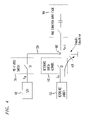
- FIG. 4 illustrates a signal flow diagram for one of the fine reference voltages in ADC 300 of FIG. 3
- FIG. 5 illustrates a timing diagram for ADC 300
- FIG. 4 shows the new signal path from S/H module 101 through pre-charge switch 301 to reference input node 403 of fine converter 104 .
- input signal 112 is also applied (in a non-switched manner) to the signal input node of fine converter 104 , as illustrated in FIG. 3 .
- switch S 1 of FIG. 4 is closed to apply pre-charge signal 320 to pre-charge parasitic capacitance 405 at reference input node 403 of fine converter 104 , while switch S 2 in reference switch network 102 is open.
- This reference voltage pre-charge process pulls the voltage of reference input node 403 of fine converter 104 to the level of input signal 112 and therefore to a level in the neighborhood of the fine reference voltage for the upcoming second phase.
- switch S 1 turns off and switch S 2 turns on ( 422 ) to apply the appropriate fine reference voltages to enable fine converter 104 to convert input signal 112 into the corresponding LSB values ( 431 ).
- the MSB and LSB values are combined together and latched out as final conversion results 117 of the ADC for Input 1.
- the above-described timing sequence is repeated to generate a digital conversion output value 117 for each successive input signal value 111 .
- Pre-charge of reference input node 403 of fine converter 104 reduces the settling error during the reference switching process in that it eliminates the input-dependent charge stored on input node 403 from the previous conversion cycle and replaces it with a voltage tracking the current input level that corresponds to a voltage close to the current fine reference level.
- the reference voltage settling process is more accurate and uniform since the difference between the initial voltage level, which is pre-charged to the current input level, and the current fine reference voltage level, is kept to within a known maximum value. This reduction in the memory effect is significant in high-speed applications where the slew rate of analog input signal 111 , and therefore the slew rate of the reference switching voltage, is high and correspondingly, the time allowed for the reference switching is short.
- this invention does not noticeably increase the power consumption and/or the die area of the ADC, since the settling accuracy of the pre-charge is simply not critical and the size of the switch devices for pre-charge could be made minimum.
- the disclosed embodiments for ADC circuits significantly reduce the reference settling error due to the memory effect with almost no area and power consumption penalty.
- a multi-stage ADC may be constructed using more than two converter modules.
- an ADC could have a coarse converter and first and second fine converters, with the second fine converter being finer than the first, where the three converters generate three different sets of bit values for the digital output.
- the coarse converter generates the first set of bit values (i.e., the MSB values)
- the input signal could be applied to pre-charge the reference input nodes at either or both of the two fine converters.
- the first fine converter generates the second set of bits (i.e., a set of intermediate bit values)
- the input signal could continue to pre-charge the reference input nodes at the second fine converter, which would next generate the LSB values.
- the present invention has been described in the context of ADCs having a reference-voltage supply consisting of a reference ladder and a reference switch network, the present invention can be implemented in the context of ADCs having other configurations of reference-voltage supplies designed to generate the reference voltages for the coarse and fine converters.
- the present invention may be implemented as circuit-based processes, including possible implementation as a single integrated circuit (such as an ASIC or an FPGA), a multi-chip module, a single card, or a multi-card circuit pack.
- a single integrated circuit such as an ASIC or an FPGA
- a multi-chip module such as a single card, or a multi-card circuit pack.
- various functions of circuit elements may also be implemented as processing steps in a software program.
- Such software may be employed in, for example, a digital signal processor, micro-controller, or general-purpose computer.
Landscapes
- Engineering & Computer Science (AREA)
- Theoretical Computer Science (AREA)
- Analogue/Digital Conversion (AREA)
Abstract
Description
Claims (24)
Priority Applications (1)
| Application Number | Priority Date | Filing Date | Title |
|---|---|---|---|
| US11/213,393 US7215274B2 (en) | 2005-07-29 | 2005-08-26 | Reference voltage pre-charge in a multi-step sub-ranging analog-to-digital converter |
Applications Claiming Priority (2)
| Application Number | Priority Date | Filing Date | Title |
|---|---|---|---|
| US70398905P | 2005-07-29 | 2005-07-29 | |
| US11/213,393 US7215274B2 (en) | 2005-07-29 | 2005-08-26 | Reference voltage pre-charge in a multi-step sub-ranging analog-to-digital converter |
Publications (2)
| Publication Number | Publication Date |
|---|---|
| US20070024484A1 US20070024484A1 (en) | 2007-02-01 |
| US7215274B2 true US7215274B2 (en) | 2007-05-08 |
Family
ID=37693739
Family Applications (1)
| Application Number | Title | Priority Date | Filing Date |
|---|---|---|---|
| US11/213,393 Expired - Fee Related US7215274B2 (en) | 2005-07-29 | 2005-08-26 | Reference voltage pre-charge in a multi-step sub-ranging analog-to-digital converter |
Country Status (1)
| Country | Link |
|---|---|
| US (1) | US7215274B2 (en) |
Cited By (15)
| Publication number | Priority date | Publication date | Assignee | Title |
|---|---|---|---|---|
| US20070252744A1 (en) * | 2006-05-01 | 2007-11-01 | Denso Corporation | A/D converter device and electronic control apparatus including same |
| US20080049825A1 (en) * | 2006-08-25 | 2008-02-28 | Broadcom Corporation | Equalizer with reorder |
| US20080049847A1 (en) * | 2006-08-25 | 2008-02-28 | Broadcom Corporation | Electronic dispersion compensation utilizing interleaved architecture and channel identification for assisting timing recovery |
| US20080069198A1 (en) * | 2006-08-25 | 2008-03-20 | Broadcom Corporation | Sequence decision feedback equalizer |
| US20080180296A1 (en) * | 2006-11-08 | 2008-07-31 | Sony Corporation | Analog-to-digital converter |
| US20080187082A1 (en) * | 2006-08-25 | 2008-08-07 | Broadcom Corporation | Electronic dispersion compensation utilizing interleaved architecture and channel identification for assisting timing recovery |
| US20090319972A1 (en) * | 2007-03-28 | 2009-12-24 | Fujitsu Microelectronics Limited | Computer program and apparatus for evaluating signal propagation delays |
| US20100103010A1 (en) * | 2008-10-28 | 2010-04-29 | Agere Systems Inc. | Two-step sub-ranging analog-to-digital converter and method for performing two-step sub-ranging in an analog-to-digital converter |
| US7755426B2 (en) | 2006-08-25 | 2010-07-13 | Broadcom Corporation | Variable gain amplifier and method for achieving variable gain amplification with high bandwidth and linearity |
| US20100182178A1 (en) * | 2009-01-20 | 2010-07-22 | Kenneth Thet Zin Oo | Two-Step Subranging ADC Architecture |
| US8300685B2 (en) | 2006-08-25 | 2012-10-30 | Broadcom Corporation | Non-linear decision feedback equalizer |
| US8502722B2 (en) | 2011-12-23 | 2013-08-06 | Industrial Technology Research Institute | Analog to digital converting apparatus and method thereof |
| US20130300459A1 (en) * | 2012-05-10 | 2013-11-14 | Pixart Imaging Inc. | Key press detecting circuit and method for detecting the status of multiple keys through a single pin |
| US10404264B2 (en) | 2017-09-11 | 2019-09-03 | Analog Devices, Inc. | Method of performing analog-to-digital conversion |
| US11239855B2 (en) * | 2020-02-11 | 2022-02-01 | Rambus Inc. | Low-noise differential-output capacitor DAC |
Families Citing this family (5)
| Publication number | Priority date | Publication date | Assignee | Title |
|---|---|---|---|---|
| US7525470B2 (en) * | 2006-08-25 | 2009-04-28 | Broadcom Corporation | Phase control for interleaved analog-to-digital conversion for electronic dispersion compensation |
| US7525462B2 (en) * | 2006-08-25 | 2009-04-28 | Broadcom Corporation | Gain control for interleaved analog-to-digital conversion for electronic dispersion compensation |
| US8483291B2 (en) * | 2011-06-30 | 2013-07-09 | Broadcom Corporation | Analog to digital converter with increased sub-range resolution |
| US9325340B2 (en) | 2014-09-02 | 2016-04-26 | Nxp, B.V. | Efficient analog to digital converter |
| US10256834B1 (en) * | 2017-09-29 | 2019-04-09 | Taiwan Semiconductor Manufacturing Company, Ltd. | Analog to digital converter |
Citations (4)
| Publication number | Priority date | Publication date | Assignee | Title |
|---|---|---|---|---|
| US6014097A (en) * | 1998-09-30 | 2000-01-11 | National Semiconductor Corporation | Fully differential interpolating comparator bank and method |
| US6177899B1 (en) * | 1998-07-29 | 2001-01-23 | Etrend Electronics, Inc. | Analog-to-digital converter having multiple reference voltage comparators and boundary voltage error correction |
| US6232907B1 (en) * | 1998-05-29 | 2001-05-15 | Texas Instruments Incorporated | Polarity shifting flash A/D converter and method |
| US6606049B1 (en) * | 2002-08-02 | 2003-08-12 | Ami Semiconductor, Inc. | Analog to digital converters based on transconveyance amplifiers |
-
2005
- 2005-08-26 US US11/213,393 patent/US7215274B2/en not_active Expired - Fee Related
Patent Citations (4)
| Publication number | Priority date | Publication date | Assignee | Title |
|---|---|---|---|---|
| US6232907B1 (en) * | 1998-05-29 | 2001-05-15 | Texas Instruments Incorporated | Polarity shifting flash A/D converter and method |
| US6177899B1 (en) * | 1998-07-29 | 2001-01-23 | Etrend Electronics, Inc. | Analog-to-digital converter having multiple reference voltage comparators and boundary voltage error correction |
| US6014097A (en) * | 1998-09-30 | 2000-01-11 | National Semiconductor Corporation | Fully differential interpolating comparator bank and method |
| US6606049B1 (en) * | 2002-08-02 | 2003-08-12 | Ami Semiconductor, Inc. | Analog to digital converters based on transconveyance amplifiers |
Cited By (28)
| Publication number | Priority date | Publication date | Assignee | Title |
|---|---|---|---|---|
| US7427936B2 (en) * | 2006-05-01 | 2008-09-23 | Denso Corporation | A/D converter device and electronic control apparatus including same |
| US20070252744A1 (en) * | 2006-05-01 | 2007-11-01 | Denso Corporation | A/D converter device and electronic control apparatus including same |
| US7755426B2 (en) | 2006-08-25 | 2010-07-13 | Broadcom Corporation | Variable gain amplifier and method for achieving variable gain amplification with high bandwidth and linearity |
| US20080049825A1 (en) * | 2006-08-25 | 2008-02-28 | Broadcom Corporation | Equalizer with reorder |
| US20080049847A1 (en) * | 2006-08-25 | 2008-02-28 | Broadcom Corporation | Electronic dispersion compensation utilizing interleaved architecture and channel identification for assisting timing recovery |
| US20080069198A1 (en) * | 2006-08-25 | 2008-03-20 | Broadcom Corporation | Sequence decision feedback equalizer |
| US8300685B2 (en) | 2006-08-25 | 2012-10-30 | Broadcom Corporation | Non-linear decision feedback equalizer |
| US20080187082A1 (en) * | 2006-08-25 | 2008-08-07 | Broadcom Corporation | Electronic dispersion compensation utilizing interleaved architecture and channel identification for assisting timing recovery |
| US7961781B2 (en) | 2006-08-25 | 2011-06-14 | Broadcom Corporation | Electronic dispersion compensation utilizing interleaved architecture and channel identification for assisting timing recovery |
| US7830987B2 (en) | 2006-08-25 | 2010-11-09 | Broadcom Corporation | Electronic dispersion compensation utilizing interleaved architecture and channel identification for assisting timing recovery |
| US7564395B2 (en) * | 2006-11-08 | 2009-07-21 | Sony Corporation | Subranging converter for converting an analog signal into an N-bit digital signal |
| US20080180296A1 (en) * | 2006-11-08 | 2008-07-31 | Sony Corporation | Analog-to-digital converter |
| US20090319972A1 (en) * | 2007-03-28 | 2009-12-24 | Fujitsu Microelectronics Limited | Computer program and apparatus for evaluating signal propagation delays |
| US8713500B2 (en) * | 2007-03-28 | 2014-04-29 | Fujitsu Semiconductor Limited | Computer program and apparatus for evaluating signal propagation delays |
| US7791523B2 (en) * | 2008-10-28 | 2010-09-07 | Agere Systems, Inc. | Two-step sub-ranging analog-to-digital converter and method for performing two-step sub-ranging in an analog-to-digital converter |
| US20100103010A1 (en) * | 2008-10-28 | 2010-04-29 | Agere Systems Inc. | Two-step sub-ranging analog-to-digital converter and method for performing two-step sub-ranging in an analog-to-digital converter |
| US9077364B2 (en) | 2009-01-20 | 2015-07-07 | Marvell World Trade Ltd. | Method and apparatus for converting an analog signal to a digital signal based on reference voltages provided by reference ladders |
| US20100182183A1 (en) * | 2009-01-20 | 2010-07-22 | Kenneth Thet Zin Oo | Reference Pre-Charging for Two-Step Subranging ADC Architecture |
| US8049652B2 (en) * | 2009-01-20 | 2011-11-01 | Marvell International Ltd. | Reference pre-charging for two-step subranging ADC architecture |
| US8077069B2 (en) * | 2009-01-20 | 2011-12-13 | Marvell World Trade Ltd. | Two-step subranging ADC architecture |
| US20100182178A1 (en) * | 2009-01-20 | 2010-07-22 | Kenneth Thet Zin Oo | Two-Step Subranging ADC Architecture |
| TWI506961B (en) * | 2009-01-20 | 2015-11-01 | Marvell World Trade Ltd | Two-step subranging adc architecture |
| US8742969B2 (en) | 2009-01-20 | 2014-06-03 | Marvell World Trade Ltd. | Two-step subranging ADC architecture |
| US8502722B2 (en) | 2011-12-23 | 2013-08-06 | Industrial Technology Research Institute | Analog to digital converting apparatus and method thereof |
| US9007097B2 (en) * | 2012-05-10 | 2015-04-14 | Pixart Imaging Inc. | Key press detecting circuit and method for detecting the status of multiple keys through a single pin |
| US20130300459A1 (en) * | 2012-05-10 | 2013-11-14 | Pixart Imaging Inc. | Key press detecting circuit and method for detecting the status of multiple keys through a single pin |
| US10404264B2 (en) | 2017-09-11 | 2019-09-03 | Analog Devices, Inc. | Method of performing analog-to-digital conversion |
| US11239855B2 (en) * | 2020-02-11 | 2022-02-01 | Rambus Inc. | Low-noise differential-output capacitor DAC |
Also Published As
| Publication number | Publication date |
|---|---|
| US20070024484A1 (en) | 2007-02-01 |
Similar Documents
| Publication | Publication Date | Title |
|---|---|---|
| US7215274B2 (en) | Reference voltage pre-charge in a multi-step sub-ranging analog-to-digital converter | |
| US7324038B2 (en) | Subranging analog to digital converter with multi-phase clock timing | |
| US7884749B2 (en) | A/D converting apparatus | |
| US8390501B2 (en) | Successive approximation register ADC with a window predictive function | |
| US9362939B1 (en) | Reduction of input dependent capacitor DAC switching current in flash-SAR analog-to-digital converters | |
| US10484000B2 (en) | Analog-to-digital converters | |
| US9148166B2 (en) | Adding predefined offset to coarse ADC residue output to SAR | |
| TWI521887B (en) | Successive approximation register anolog-to-digital converter | |
| US20070290915A1 (en) | Pipeline A/D converter conterting analog signal to digital signal | |
| US8542144B2 (en) | Analog to digital converter | |
| US10530382B2 (en) | Successive approximation register analog-to-digital converter and conversion method therefor | |
| US6229472B1 (en) | A/D converter | |
| US7821436B2 (en) | System and method for reducing power dissipation in an analog to digital converter | |
| US7102559B2 (en) | Analog-to-digital converter having interleaved coarse sections coupled to a single fine section | |
| JP4684028B2 (en) | Pipeline A / D converter | |
| US10812098B1 (en) | Analog-to-digital converter decision control | |
| US10547321B2 (en) | Method and apparatus for enabling wide input common-mode range in SAR ADCS with no additional active circuitry | |
| US8921790B2 (en) | IR detector system and method | |
| US6700523B2 (en) | Analog to digital converter selecting reference voltages in accordance with feedback from prior stages | |
| US20040257257A1 (en) | A/D converter and A/D conversion method | |
| JP4236519B2 (en) | A / D converter | |
| Lee et al. | Offset and dynamic gain-mismatch reduction techniques for 10b 200ms/s parallel pipeline ADCs | |
| Shen et al. | A 0.0033 mm 2 3.5 fJ/conversion-step SAR ADC with 2× Input Range Boosting | |
| US20220123761A1 (en) | Analog-to-digital converter | |
| JPH0879078A (en) | Series-parallel a/d converter |
Legal Events
| Date | Code | Title | Description |
|---|---|---|---|
| AS | Assignment |
Owner name: AGERE SYSTEMS, INC., PENNSYLVANIA Free format text: ASSIGNMENT OF ASSIGNORS INTEREST;ASSIGNOR:LIU, SONG;REEL/FRAME:016921/0321 Effective date: 20050823 |
|
| FEPP | Fee payment procedure |
Free format text: PAYOR NUMBER ASSIGNED (ORIGINAL EVENT CODE: ASPN); ENTITY STATUS OF PATENT OWNER: LARGE ENTITY |
|
| FPAY | Fee payment |
Year of fee payment: 4 |
|
| AS | Assignment |
Owner name: DEUTSCHE BANK AG NEW YORK BRANCH, AS COLLATERAL AG Free format text: PATENT SECURITY AGREEMENT;ASSIGNORS:LSI CORPORATION;AGERE SYSTEMS LLC;REEL/FRAME:032856/0031 Effective date: 20140506 |
|
| REMI | Maintenance fee reminder mailed | ||
| AS | Assignment |
Owner name: AVAGO TECHNOLOGIES GENERAL IP (SINGAPORE) PTE. LTD Free format text: ASSIGNMENT OF ASSIGNORS INTEREST;ASSIGNOR:AGERE SYSTEMS LLC;REEL/FRAME:035365/0634 Effective date: 20140804 |
|
| LAPS | Lapse for failure to pay maintenance fees | ||
| STCH | Information on status: patent discontinuation |
Free format text: PATENT EXPIRED DUE TO NONPAYMENT OF MAINTENANCE FEES UNDER 37 CFR 1.362 |
|
| FP | Lapsed due to failure to pay maintenance fee |
Effective date: 20150508 |
|
| AS | Assignment |
Owner name: LSI CORPORATION, CALIFORNIA Free format text: TERMINATION AND RELEASE OF SECURITY INTEREST IN PATENT RIGHTS (RELEASES RF 032856-0031);ASSIGNOR:DEUTSCHE BANK AG NEW YORK BRANCH, AS COLLATERAL AGENT;REEL/FRAME:037684/0039 Effective date: 20160201 Owner name: AGERE SYSTEMS LLC, PENNSYLVANIA Free format text: TERMINATION AND RELEASE OF SECURITY INTEREST IN PATENT RIGHTS (RELEASES RF 032856-0031);ASSIGNOR:DEUTSCHE BANK AG NEW YORK BRANCH, AS COLLATERAL AGENT;REEL/FRAME:037684/0039 Effective date: 20160201 |