US7106130B2 - Variable frequency PWM controller circuit - Google Patents
Variable frequency PWM controller circuit Download PDFInfo
- Publication number
- US7106130B2 US7106130B2 US10/656,420 US65642003A US7106130B2 US 7106130 B2 US7106130 B2 US 7106130B2 US 65642003 A US65642003 A US 65642003A US 7106130 B2 US7106130 B2 US 7106130B2
- Authority
- US
- United States
- Prior art keywords
- signal
- pwm
- ramp signal
- ramp
- error
- Prior art date
- Legal status (The legal status is an assumption and is not a legal conclusion. Google has not performed a legal analysis and makes no representation as to the accuracy of the status listed.)
- Expired - Lifetime, expires
Links
- 238000000034 method Methods 0.000 claims description 10
- 239000003990 capacitor Substances 0.000 claims description 9
- 230000000630 rising effect Effects 0.000 claims description 3
- 230000007274 generation of a signal involved in cell-cell signaling Effects 0.000 claims 3
- 230000001360 synchronised effect Effects 0.000 description 10
- 230000003247 decreasing effect Effects 0.000 description 4
- 230000001105 regulatory effect Effects 0.000 description 4
- 230000008901 benefit Effects 0.000 description 3
- 238000006243 chemical reaction Methods 0.000 description 2
- 238000013016 damping Methods 0.000 description 2
- 238000007599 discharging Methods 0.000 description 2
- 230000004075 alteration Effects 0.000 description 1
- 230000033228 biological regulation Effects 0.000 description 1
- 238000010586 diagram Methods 0.000 description 1
- 230000006872 improvement Effects 0.000 description 1
- 238000012986 modification Methods 0.000 description 1
- 230000004048 modification Effects 0.000 description 1
- 230000008569 process Effects 0.000 description 1
Images


Classifications
-
- H—ELECTRICITY
- H02—GENERATION; CONVERSION OR DISTRIBUTION OF ELECTRIC POWER
- H02M—APPARATUS FOR CONVERSION BETWEEN AC AND AC, BETWEEN AC AND DC, OR BETWEEN DC AND DC, AND FOR USE WITH MAINS OR SIMILAR POWER SUPPLY SYSTEMS; CONVERSION OF DC OR AC INPUT POWER INTO SURGE OUTPUT POWER; CONTROL OR REGULATION THEREOF
- H02M3/00—Conversion of dc power input into dc power output
- H02M3/02—Conversion of dc power input into dc power output without intermediate conversion into ac
- H02M3/04—Conversion of dc power input into dc power output without intermediate conversion into ac by static converters
- H02M3/10—Conversion of dc power input into dc power output without intermediate conversion into ac by static converters using discharge tubes with control electrode or semiconductor devices with control electrode
- H02M3/145—Conversion of dc power input into dc power output without intermediate conversion into ac by static converters using discharge tubes with control electrode or semiconductor devices with control electrode using devices of a triode or transistor type requiring continuous application of a control signal
- H02M3/155—Conversion of dc power input into dc power output without intermediate conversion into ac by static converters using discharge tubes with control electrode or semiconductor devices with control electrode using devices of a triode or transistor type requiring continuous application of a control signal using semiconductor devices only
- H02M3/156—Conversion of dc power input into dc power output without intermediate conversion into ac by static converters using discharge tubes with control electrode or semiconductor devices with control electrode using devices of a triode or transistor type requiring continuous application of a control signal using semiconductor devices only with automatic control of output voltage or current, e.g. switching regulators
-
- H—ELECTRICITY
- H02—GENERATION; CONVERSION OR DISTRIBUTION OF ELECTRIC POWER
- H02M—APPARATUS FOR CONVERSION BETWEEN AC AND AC, BETWEEN AC AND DC, OR BETWEEN DC AND DC, AND FOR USE WITH MAINS OR SIMILAR POWER SUPPLY SYSTEMS; CONVERSION OF DC OR AC INPUT POWER INTO SURGE OUTPUT POWER; CONTROL OR REGULATION THEREOF
- H02M1/00—Details of apparatus for conversion
- H02M1/0003—Details of control, feedback or regulation circuits
- H02M1/0032—Control circuits allowing low power mode operation, e.g. in standby mode
-
- H—ELECTRICITY
- H03—ELECTRONIC CIRCUITRY
- H03K—PULSE TECHNIQUE
- H03K3/00—Circuits for generating electric pulses; Monostable, bistable or multistable circuits
- H03K3/02—Generators characterised by the type of circuit or by the means used for producing pulses
- H03K3/023—Generators characterised by the type of circuit or by the means used for producing pulses by the use of differential amplifiers or comparators, with internal or external positive feedback
- H03K3/0231—Astable circuits
-
- Y—GENERAL TAGGING OF NEW TECHNOLOGICAL DEVELOPMENTS; GENERAL TAGGING OF CROSS-SECTIONAL TECHNOLOGIES SPANNING OVER SEVERAL SECTIONS OF THE IPC; TECHNICAL SUBJECTS COVERED BY FORMER USPC CROSS-REFERENCE ART COLLECTIONS [XRACs] AND DIGESTS
- Y02—TECHNOLOGIES OR APPLICATIONS FOR MITIGATION OR ADAPTATION AGAINST CLIMATE CHANGE
- Y02B—CLIMATE CHANGE MITIGATION TECHNOLOGIES RELATED TO BUILDINGS, e.g. HOUSING, HOUSE APPLIANCES OR RELATED END-USER APPLICATIONS
- Y02B70/00—Technologies for an efficient end-user side electric power management and consumption
- Y02B70/10—Technologies improving the efficiency by using switched-mode power supplies [SMPS], i.e. efficient power electronics conversion e.g. power factor correction or reduction of losses in power supplies or efficient standby modes
Definitions
- the present invention relates to switching mode power supplies, and more specifically to a varied frequency pulse width modulation controller for low standby loss solution.
- a flyback converter is the most commonly used topology for this application with pulse width modulation (PWM) control for the output regulation.
- PWM pulse width modulation
- the conventional PWM controller circuit always operates at a constant frequency, corresponding to the switching period T as shown in FIG. 1 , which shows the operating PWM signal for the normal and standby operation mode respectively.
- the power circuit operates with relatively a long on time PWM, Ton,nor, and thus a high duty cycle under normal load condition.
- Ton,sb In the standby operation mode, the power circuit always operates with relatively a very short time Ton,sb and thus a very small duty cycle, but the switching frequency is still high as normal operation, resulting in relatively much switching loss and driving loss of the main switch and much power loss of the controller which are the major parts of the standby loss. Therefore, the standby loss of the converter will be relatively high.
- the advantage of the PWM controller circuit is that the output ripple and noise are relatively very low even at the standby operation mode.
- the switching related loss which is the main component of the standby loss.
- One is to decrease the switching frequency by regulating the Toff time of the PWM signal while keeping a constant Ton time of the PWM signal for standby operation.
- Ton,sb which is equal to the counterpart Ton,nor for the normal operation mode.
- Toff time is regulated as Toff,sb, which is relatively much longer than that Toff,nor for the normal operation mode.
- the switching period is relatively much longer than that of the normal operation mode and the switching frequency is relatively much lower which benefits to the relatively low standby loss in the standby operation mode as mentioned before.
- the other method is a burst mode control for the standby operation mode.
- the PWM signal In the normal operation mode, the PWM signal is relatively with a high frequency and long on time as Ton,nor.
- Ton,nor In the standby operation mode, the on time of PWM signal can be regulated relatively short as Ton,sb at each switching period, but after several continuous switching periods, some switching periods will be skipped. Therefore, in the standby operation mode, the equivalent switching period will be Tsb/n, where n is the numbers of PWM pulses during the Tsb time. It can be seen that, in the standby operation mode, the equivalent switching period of the PWM signal is longer than that of the normal operation mode. So, the switching related loss can be effectively reduced and thus the relatively low standby loss can be achieved.
- each of the PWM signals will have relatively a long on time Ton,nor and a short switching period Tnor in the normal operation mode according to the present invention.
- the duty cycle Dnor which is equal to Ton,nor/Tnor
- the switching frequency fnor which is equal to 1/Tnor
- the on time of the PWM signal is decreased while the off time of the PWM signal is increased.
- the on time Ton,sb of the PWM signal is reduced to a relatively low value, the off time Toff,sb and thus the switching period Tsb are increased to a relatively high value in the standby operation mode. Therefore, relatively very low duty cycle and very low switching frequency can be achieved in the standby operation mode of the power converter, wherein relatively low standby loss, low output voltage noise and no audible noise are realized simultaneously.
- a circuit generating a wide range of variable frequency (VF) PWM control signals is provided.
- An error-amplified voltage V E/A is generated by a feedback loop. And then this V E/A is input into a ramp generator.
- the ramp generator is composed of a controllable charge current source, a controllable discharge current source, and a timing capacitor. These two current sources charge and discharge the timing capacitor, which generates a ramp signal.
- a PWM comparator, and a hysteretic voltage comparator will be employed to process this ramp signal and generate a PWM signal.
- the controllable charge current source and controllable discharge current source are controlled by the value of the error-amplified voltage V E/A .
- the lower the error-amplified voltage V E/A is, the higher the charge current and the lower the discharge current will be. Relatively, the rising time of the ramp signal will be shorter, and the descending time will be longer. Therefore, the generated PWM signal features relatively a lower duty cycle and a lower frequency.
- the present invention allows relatively a low duty cycle and a low frequency operation, which makes a power converter operate with relatively low ripple, low noise and low standby loss. This is a significant improvement over the prior art.
- FIG. 1 shows a PWM signal generating scheme of a conventional PWM controller
- FIG. 2 shows a frequency decreasing PWM signal generating scheme for low standby loss
- FIG. 3 shows a burst mode PWM signal generating scheme for low standby loss
- FIG. 4 shows a PWM signal generating scheme for low standby loss according to the present invention
- FIG. 5 shows a preferred embodiment of the controller circuit according to the present invention
- FIG. 6 shows the operation waveforms of the controller circuit according to the first preferred embodiment of the present invention
- FIG. 7 shows another preferred embodiment of the controller circuit according to the present invention.
- FIG. 8 shows the operation waveforms of the controller circuit according to the second preferred embodiment of the present invention.
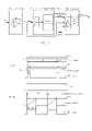
- FIG. 5 a circuit diagram to realize the VF PWM control scheme according to the present invention is shown.
- the overall circuit of the invention has three parts including a feedback loop, a synchronous signal generator and a PWM comparator.
- the output voltage is input to the feedback loop which in-turn outputs an error-amplified voltage V E/A .
- the V E/A signal is firstly input to a synchronous signal generator, which includes a VCO (Voltage Control Oscillator) and selectively includes a pulse generator, which is an optional component coupled to the VCO and can be omitted without damping the functions of the synchronous generator, and outputs a variable frequency synchronous signal according to the value of the V E/A signal.
- the PWM comparator including a comparator AP and a RS flip flop, with the synchronous signal, the V E/A signal and a ramp signal as inputs and generates a PWM signal.
- the operation waveforms can be illustrated in FIG. 6 a and FIG. 6 b , wherein FIG. 6 a shows the standby operation mode and FIG. 6 b shows the normal operation mode.
- the V E/A signal has relatively low value.
- the VCO of the synchronous signal generator produces a relatively low frequency oscillating waveform to the pulse generator according to the value of the V E/A signal.
- the pulse generator outputs a pulse with this relatively low frequency, 1/Tsb, to the PWM comparator as the synchronous signal.
- the synchronous signal is coupled to the S terminal of the RS flip-flop.
- the V E/A signal is coupled to one input of the comparator AP of the PWM comparator and a ramp signal is coupled to another input of the comparator AP.
- the ramp signal can be a current signal of the main switch of the power converter.
- the voltage of the V E/A signal is relatively high.
- the generated synchronous signal will have relatively a high frequency corresponding to a low period as Tnor.
- the PWM signal will have a relatively long on time shown as Ton,nor.
- Ton,nor the PWM signal features relatively the high frequency and high duty cycle at normal operation mode.
- FIG. 7 another controller circuit according to the present invention is shown, in which the off time and the on time of the generated PWM signal are changed with the error-amplified voltage simultaneously.
- a PWM signal with relatively a very low duty cycle and a low frequency can be generated by this means.
- the overall circuit of this invention comprises three parts: a feedback loop, which inputs with an output voltage Vo of a switching mode power converter (not shown) and outputs an error-amplified voltage V E/A , a ramp generator, and a PWM comparator.
- the ramp generator is formed with a charge current source I c , a discharge current source I d , and a timing capacitor CT.
- V H and V L are connected to a noninverting terminal of the comparator A 1 and an inverting terminal of the comparator A 2 respectively.
- the output voltage Vo of the switching mode power converter is input into the feedback loop.
- An error-amplified voltage is generated by the feedback loop as V E/A .
- V E/A As the conventional design of the feedback loop, when the output load is high, V E/A will be high relatively.
- the V E/A voltage controls the charge current source I c and the discharge current source I d .
- the voltage of the V E/A controls the values of I c and I d .
- the output PWM signal which is an optional input of the ramp generator, can be selectively omitted without damping the functions of the ramp generator.
- V E/A When V E/A is high, the value of I c of the ramp generator will be high and the value of its I d will be low relatively.
- FIG. 8 a and FIG. 8 b show the standby operation mode and FIG. 8 b shows the normal operation mode.
- the charge current I c will be high in the standby operation mode due to the relatively low V E/A .
- the Ton time of the PWM signal which is the time of the charge current I c charging the voltage across CT from V L to V H
- the discharge current I d is relatively low
- the Toff time of the PWM signal which is the time of the discharge current I d discharging the voltage across CT from V H to V L
- the Ton time of the PWM signal will be relatively long while Toff time is relatively short.
- this PWTM controller features with relatively a high switching frequency and a high duty cycle under the normal load operation, and a low switching frequency and a low duty cycle under the light load operation with this second embodiment of the present invention.
- the switching mode converter can be designed with relatively high frequency, which benefits to high power density. At light load, the converter will be operated in relatively a low switching frequency and a low duty cycle, therefore, a relatively low standby loss with low output ripple.
- the charging and discharging of I c and I d can be modulated by output PWM signal.
Landscapes
- Engineering & Computer Science (AREA)
- Power Engineering (AREA)
- Dc-Dc Converters (AREA)
Abstract
The present invention discloses a circuit that generates a variable frequency pulse width modulation (VF PWM) signal. Different from the conventional PWM controller, the frequency and duty cycle of the output PWM signal vary with the error-amplified voltage of the feedback loop simultaneously in this invention. The higher the error-amplified voltage of the feedback loop is, the lower the duty cycle with lower frequency will be. A very low duty cycle PWM signal can be generated stably while its frequency is very low.
Description
The present invention relates to switching mode power supplies, and more specifically to a varied frequency pulse width modulation controller for low standby loss solution.
The trend in the design of switching mode power supplies has been toward relatively low power loss, low ripple and low noise under light load condition, especially for those widely used adaptors for notebooks, computers, and chargers for mobile telecommunication apparatus. This kind of power supplies frequently operates under a light or zero load condition, which is named as the standby operation mode.
A flyback converter is the most commonly used topology for this application with pulse width modulation (PWM) control for the output regulation. To achieve relatively very low power loss under light or open load condition, it is the key factor to control the power stage to operate at a relatively very low switching frequency to decrease the switching loss and driving loss of the generally used MOSFET power switch. Meanwhile, the control circuit dissipates relatively low loss due to relatively low frequency operation.
The conventional PWM controller circuit according to the general prior art always operates at a constant frequency, corresponding to the switching period T as shown in FIG. 1 , which shows the operating PWM signal for the normal and standby operation mode respectively. The power circuit operates with relatively a long on time PWM, Ton,nor, and thus a high duty cycle under normal load condition. In the standby operation mode, the power circuit always operates with relatively a very short time Ton,sb and thus a very small duty cycle, but the switching frequency is still high as normal operation, resulting in relatively much switching loss and driving loss of the main switch and much power loss of the controller which are the major parts of the standby loss. Therefore, the standby loss of the converter will be relatively high. However the advantage of the PWM controller circuit is that the output ripple and noise are relatively very low even at the standby operation mode.
Moreover, there are generally two methods to decrease the switching related loss which is the main component of the standby loss. One is to decrease the switching frequency by regulating the Toff time of the PWM signal while keeping a constant Ton time of the PWM signal for standby operation. Please refer to FIG. 2 . In the standby operation mode, the constant switching on time of PWM signal is Ton,sb, which is equal to the counterpart Ton,nor for the normal operation mode. But the Toff time is regulated as Toff,sb, which is relatively much longer than that Toff,nor for the normal operation mode. As a result, the switching period is relatively much longer than that of the normal operation mode and the switching frequency is relatively much lower which benefits to the relatively low standby loss in the standby operation mode as mentioned before.
One drawback of this control method is that the conversion power at each switching cycle will be relatively high due to the constant on time of the PWM signal in the standby operation mode. Therefore, relatively high output voltage noise and even audible noise might be introduced to the converter though the standby loss can be effectively reduced.
The other method is a burst mode control for the standby operation mode. Please refer to FIG. 3 for the operation PWM signal with this control mode. In the normal operation mode, the PWM signal is relatively with a high frequency and long on time as Ton,nor. In the standby operation mode, the on time of PWM signal can be regulated relatively short as Ton,sb at each switching period, but after several continuous switching periods, some switching periods will be skipped. Therefore, in the standby operation mode, the equivalent switching period will be Tsb/n, where n is the numbers of PWM pulses during the Tsb time. It can be seen that, in the standby operation mode, the equivalent switching period of the PWM signal is longer than that of the normal operation mode. So, the switching related loss can be effectively reduced and thus the relatively low standby loss can be achieved.
But there are problems with this control mode also. In the standby operation mode, the conversion power of the converter during the several continuous switching periods with PWM pulses will be relatively high, resulting in relatively high output voltage noise. Meanwhile, the several continuous switching periods with PWM pulses occur during a relatively long Tsb period corresponding to a relatively low frequency. This will also introduces the audible noise to the converter.
It is therefore attempted by the applicant to deal with the above situation encountered with the prior art.
A new PWM signal generating scheme is presented, as shown in FIG. 4 . The on time and the off time of the PWM signal are regulated simultaneously according to the scheme. Each of the generated PWM signals will have relatively a very short on time and a very low frequency in the standby operation mode, and have relatively a high frequency and a long on time in the normal operation mode, thus the aforementioned ripple and noise can be eliminated while the relatively low standby loss feature is maintained.
In more details, each of the PWM signals will have relatively a long on time Ton,nor and a short switching period Tnor in the normal operation mode according to the present invention. Thus, the duty cycle Dnor, which is equal to Ton,nor/Tnor, is relatively high and the switching frequency fnor, which is equal to 1/Tnor, is relatively high too. These relatively high duty cycle and high switching frequency are advantageous to the relatively high power density and high efficiency design of the power converter.
As the load decreasing, the on time of the PWM signal is decreased while the off time of the PWM signal is increased. As a result, the on time Ton,sb of the PWM signal is reduced to a relatively low value, the off time Toff,sb and thus the switching period Tsb are increased to a relatively high value in the standby operation mode. Therefore, relatively very low duty cycle and very low switching frequency can be achieved in the standby operation mode of the power converter, wherein relatively low standby loss, low output voltage noise and no audible noise are realized simultaneously.
In accordance with the preferred embodiment of the present invention, a circuit generating a wide range of variable frequency (VF) PWM control signals is provided. An error-amplified voltage VE/A is generated by a feedback loop. And then this VE/A is input into a ramp generator. The ramp generator is composed of a controllable charge current source, a controllable discharge current source, and a timing capacitor. These two current sources charge and discharge the timing capacitor, which generates a ramp signal. Typically, a PWM comparator, and a hysteretic voltage comparator will be employed to process this ramp signal and generate a PWM signal.
The controllable charge current source and controllable discharge current source are controlled by the value of the error-amplified voltage VE/A. Corresponding to the load decreasing condition, the lower the error-amplified voltage VE/A is, the higher the charge current and the lower the discharge current will be. Relatively, the rising time of the ramp signal will be shorter, and the descending time will be longer. Therefore, the generated PWM signal features relatively a lower duty cycle and a lower frequency.
The present invention allows relatively a low duty cycle and a low frequency operation, which makes a power converter operate with relatively low ripple, low noise and low standby loss. This is a significant improvement over the prior art.
The present invention may best be understood through the following description with reference to the accompanying drawings, in which:
Although this invention is susceptible to embodiments of many different forms, a preferred embodiment will be described and illustrated in detail herein. The present disclosure exemplifies the principle of the invention and is not being considered a limitation to the broader aspects of the invention to the particular embodiment as described.
In FIG. 5 , a circuit diagram to realize the VF PWM control scheme according to the present invention is shown. The overall circuit of the invention has three parts including a feedback loop, a synchronous signal generator and a PWM comparator.
The output voltage is input to the feedback loop which in-turn outputs an error-amplified voltage VE/A. The VE/A signal is firstly input to a synchronous signal generator, which includes a VCO (Voltage Control Oscillator) and selectively includes a pulse generator, which is an optional component coupled to the VCO and can be omitted without damping the functions of the synchronous generator, and outputs a variable frequency synchronous signal according to the value of the VE/A signal. The PWM comparator, including a comparator AP and a RS flip flop, with the synchronous signal, the VE/A signal and a ramp signal as inputs and generates a PWM signal.
The operation waveforms can be illustrated in FIG. 6 a and FIG. 6 b, wherein FIG. 6 a shows the standby operation mode and FIG. 6 b shows the normal operation mode. In the standby operation mode, the VE/A signal has relatively low value. As a result, the VCO of the synchronous signal generator produces a relatively low frequency oscillating waveform to the pulse generator according to the value of the VE/A signal. Then, the pulse generator outputs a pulse with this relatively low frequency, 1/Tsb, to the PWM comparator as the synchronous signal. In more details, the synchronous signal is coupled to the S terminal of the RS flip-flop. Meanwhile, the VE/A signal is coupled to one input of the comparator AP of the PWM comparator and a ramp signal is coupled to another input of the comparator AP. Hereby, the ramp signal can be a current signal of the main switch of the power converter. Once the synchronous signal triggers the RS flip-flop, the PWM signal begins its high level till the voltage of the ramp signal rises to equal with the voltage of VE/A signal. This time duration, shown as Ton,sb which is the on time of the PWM signal, is relatively very low because of the relatively low voltage of the VE/A signal in the standby operation mode. Therefore, the output PWM signal will have a relatively short on time Ton,sb and a relatively low frequency.
As to the normal operation mode with the operations waveforms shown in FIG. 6 b, the voltage of the VE/A signal is relatively high. With the same scheme as aforementioned in the standby operation mode, the generated synchronous signal will have relatively a high frequency corresponding to a low period as Tnor. While the PWM signal will have a relatively long on time shown as Ton,nor. Thus the PWM signal features relatively the high frequency and high duty cycle at normal operation mode.
In FIG. 7 , another controller circuit according to the present invention is shown, in which the off time and the on time of the generated PWM signal are changed with the error-amplified voltage simultaneously. A PWM signal with relatively a very low duty cycle and a low frequency can be generated by this means.
The overall circuit of this invention comprises three parts: a feedback loop, which inputs with an output voltage Vo of a switching mode power converter (not shown) and outputs an error-amplified voltage VE/A, a ramp generator, and a PWM comparator.
The ramp generator is formed with a charge current source Ic, a discharge current source Id, and a timing capacitor CT.
Two comparators, shown in FIG. 7 as A1 and A2, and a RS flip-flop make up the PWM comparator. VH and VL, as a high reference voltage and a low reference voltage respectively, are connected to a noninverting terminal of the comparator A1 and an inverting terminal of the comparator A2 respectively.
The output voltage Vo of the switching mode power converter is input into the feedback loop. An error-amplified voltage is generated by the feedback loop as VE/A. As the conventional design of the feedback loop, when the output load is high, VE/A will be high relatively. The VE/A voltage controls the charge current source Ic and the discharge current source Id. The voltage of the VE/A controls the values of Ic and Id. The output PWM signal, which is an optional input of the ramp generator, can be selectively omitted without damping the functions of the ramp generator. When VE/A is high, the value of Ic of the ramp generator will be high and the value of its Id will be low relatively.
The operation waveforms can be illustrated in FIG. 8 a and FIG. 8 b, wherein FIG. 8 a shows the standby operation mode and FIG. 8 b shows the normal operation mode. It can be seen from the aforementioned analysis, the charge current Ic will be high in the standby operation mode due to the relatively low VE/A. Thus, the Ton time of the PWM signal, which is the time of the charge current Ic charging the voltage across CT from VL to VH, will be relatively short. Meanwhile, the discharge current Id is relatively low and the Toff time of the PWM signal, which is the time of the discharge current Id discharging the voltage across CT from VH to VL, will be relatively long. Please refer to FIG. 8 b. With the same principle, when the converter operates under a normal load condition, the Ton time of the PWM signal will be relatively long while Toff time is relatively short.
As a result, this PWTM controller features with relatively a high switching frequency and a high duty cycle under the normal load operation, and a low switching frequency and a low duty cycle under the light load operation with this second embodiment of the present invention.
Therefore, with the PWM control of the present invention, the switching mode converter can be designed with relatively high frequency, which benefits to high power density. At light load, the converter will be operated in relatively a low switching frequency and a low duty cycle, therefore, a relatively low standby loss with low output ripple. For low control circuit loss at standby mode operation, the charging and discharging of Ic and Id can be modulated by output PWM signal. When the PWM signal is in a high voltage level, the Ic is set to the value as aforementioned while the value of Id is set to zero. When the PWM signal is in a low voltage level, the Id is set to the value as aforementioned while the value of Ic is set to zero.
Although the present invention has been described in terms of the presently preferred embodiment, it is to be understood that such disclosure is not to be interpreted as limiting. Various alterations and modifications will no doubt become apparent to those skilled in the art after having read the above disclosure.
Claims (11)
1. A circuit that generates a ramp signal used in a pulse width modulation (PWM) signal generation, comprising:
a feedback loop for generating an error-amplified voltage; and
a ramp generator coupled to said feedback loop for receiving said error-amplified voltage and being controlled by said error-amplified voltage to generate said ramp signal,
wherein said ramp generator comprises:
a timing capacitor to be charged and discharged for generating said ramp signal;
a charge current source in which its magnitude is controlled by said error-amplified voltage so as to charge said timing capacitor and generate a rising slope of said ramp signal; and
a discharge current source in which its magnitude is controlled by said error-amplified voltage so as to discharge said timing capacitor and generate a descending slope of said ramp signal.
2. The circuit according to claim 1 , wherein said circuit further comprises a PWM comparator coupled to said ramp generator for receiving said ramp signal to generate said PWM signal.
3. The circuit according to claim 2 , wherein said PWM signal is selectively input to said ramp generator with said error-amplified voltage so as to generate said ramp signal.
4. The circuit according to claim 2 , wherein said PWM comparator comprises:
a first comparator coupled its inverting input to said ramp signal and its noninverting input to a high level reference voltage for comparing said ramp signal with said high level reference voltage to produce a first comparison output;
a second comparator coupled its noninverting input to said ramp signal and its inverting input to a low level reference voltage for comparing said ramp signal with said low level reference voltage to produce a second comparison output; and
a flip-flop circuit coupled to an output of said first and second comparators for generating said PWM signal.
5. The circuit according to claim 2 , wherein said PWM comparator is a hysteretic comparator.
6. A ramp signal generation method used in a pulse width modulation (PWM) signal generation employing a circuit comprising a feedback loop and a ramp generator with a charge current source, a timing capacitor and a discharge current source, comprising steps of:
generating an error-amplified voltage from said feedback loop;
controlling said charge current source to charge said timing capacitor and generate a rising slope of said ramp signal in which said charge current source's magnitude is controlled by said error-amplified voltage and said charge current source's power on state is controlled by a high level of a PWM signal; and
controlling said discharge current source to discharge said timing capacitor and generate a descending slope of said ramp signal in which said discharge current source's magnitude is controlled by said error-amplified voltage and said discharge current source's power on state is controlled by a low level of said PWM signal.
7. The method according to claim 6 , wherein said ramp generator is coupled to said feedback loop for receiving said error-amplified voltage and being controlled by said error-amplified voltage to generate said ramp signal.
8. The method according to claim 6 wherein said circuit further comprises a PWM comparator coupled to said ramp generator for receiving said ramp signal to generate said PWM signal.
9. The method according to claim 8 , wherein said PWM signal is selectively input to said ramp generator with said error-amplified voltage so as to generate said ramp signal.
10. The method according to claim 8 , wherein said PWM comparator comprises:
a first comparator coupled its inverting input to said ramp signal and its noninverting input to a high level reference voltage for comparing said ramp signal with said high level reference voltage to produce a first comparison output;
a second comparator coupled its noninverting input to said ramp signal and its inverting input to a low level reference voltage for comparing said ramp signal with said low level reference voltage to produce a second comparison output; and
a flip-flop circuit coupled to an output of said first and second comparators for generating said PWM signal.
11. The method according to claim 8 , wherein said PWM comparator is a hysteretic comparator.
Priority Applications (3)
| Application Number | Priority Date | Filing Date | Title |
|---|---|---|---|
| US10/656,420 US7106130B2 (en) | 2003-09-05 | 2003-09-05 | Variable frequency PWM controller circuit |
| TW093126808A TWI271037B (en) | 2003-09-05 | 2004-09-03 | Variable frequency PWM controller circuit |
| CNB2004100769458A CN100342629C (en) | 2003-09-05 | 2004-09-03 | Variable frequency PWM controller circuit |
Applications Claiming Priority (1)
| Application Number | Priority Date | Filing Date | Title |
|---|---|---|---|
| US10/656,420 US7106130B2 (en) | 2003-09-05 | 2003-09-05 | Variable frequency PWM controller circuit |
Publications (2)
| Publication Number | Publication Date |
|---|---|
| US20050052249A1 US20050052249A1 (en) | 2005-03-10 |
| US7106130B2 true US7106130B2 (en) | 2006-09-12 |
Family
ID=34226330
Family Applications (1)
| Application Number | Title | Priority Date | Filing Date |
|---|---|---|---|
| US10/656,420 Expired - Lifetime US7106130B2 (en) | 2003-09-05 | 2003-09-05 | Variable frequency PWM controller circuit |
Country Status (3)
| Country | Link |
|---|---|
| US (1) | US7106130B2 (en) |
| CN (1) | CN100342629C (en) |
| TW (1) | TWI271037B (en) |
Cited By (21)
| Publication number | Priority date | Publication date | Assignee | Title |
|---|---|---|---|---|
| US20060152184A1 (en) * | 2005-01-13 | 2006-07-13 | Yuichi Matsushita | Pulse width modulation circuit |
| US20060250191A1 (en) * | 2005-05-05 | 2006-11-09 | Alan Daniel | Apparatus and method for reducing power consumption within an oscillator |
| US20080048789A1 (en) * | 2006-08-25 | 2008-02-28 | Ameritherm, Inc. | Automatic Frequency Compensation for Pulse Width Modulated RF Level Control |
| US20080074183A1 (en) * | 2006-09-26 | 2008-03-27 | Tai-1 Microelectronics Corp. | Compensated gain control device |
| US20080094049A1 (en) * | 2006-10-20 | 2008-04-24 | Wenkai Wu | PWM modulator for scalable converters |
| US20080158760A1 (en) * | 2004-08-23 | 2008-07-03 | Monolithic Power Systems, Inc. | Method and apparatus for fault detection scheme for cold cathode florescent lamp (ccfl) integrated circuits |
| US20090273330A1 (en) * | 2008-04-30 | 2009-11-05 | International Rectifier Corporation | Merged ramp/oscillator for precise ramp control in one cycle pfc converter |
| US20090302911A1 (en) * | 2008-06-06 | 2009-12-10 | Niko Semiconductor Co., Ltd. | Frequency jitter generator and pwm controller |
| US20100141033A1 (en) * | 2008-12-10 | 2010-06-10 | Yen-Hui Wang | Efficient pwm controller |
| US20110068763A1 (en) * | 2006-09-07 | 2011-03-24 | Richtek Technology Corp. | Duty feed forward method and apparatus for modulating a duty of a pmw signal and power converting method and power converter using the same |
| US8063570B2 (en) | 2007-11-29 | 2011-11-22 | Monolithic Power Systems, Inc. | Simple protection circuit and adaptive frequency sweeping method for CCFL inverter |
| US20110291575A1 (en) * | 2010-05-25 | 2011-12-01 | Green Solution Technology Co., Ltd. | Led driving circuit and control circuit |
| US8164293B2 (en) | 2009-09-08 | 2012-04-24 | Hoffman Enclosures, Inc. | Method of controlling a motor |
| US8183810B2 (en) | 2009-09-08 | 2012-05-22 | Hoffman Enclosures, Inc. | Method of operating a motor |
| US8297369B2 (en) | 2009-09-08 | 2012-10-30 | Sta-Rite Industries, Llc | Fire-extinguishing system with servo motor-driven foam pump |
| US20130027012A1 (en) * | 2011-07-27 | 2013-01-31 | Upi Semiconductor Corp. | Dc-dc converter and voltage conversion method thereof |
| US20130093515A1 (en) * | 2010-12-15 | 2013-04-18 | Liang Cheng | Pwm comparator and class d amplifier |
| US20130127557A1 (en) * | 2011-11-21 | 2013-05-23 | Intersil Americas LLC | System and method of maintaining gain linearity of variable frequency modulator |
| US8493047B2 (en) | 2011-05-23 | 2013-07-23 | Alpha And Omega Semiconductor Incorporated | Constant on-time switching regulator implementing dual control loops |
| US20140225583A1 (en) * | 2011-07-27 | 2014-08-14 | Upi Semiconductor Corp. | Dc-dc converter and voltage conversion method thereof |
| US11005455B2 (en) * | 2019-04-04 | 2021-05-11 | Silanna Asia Pte Ltd | Generating voltage pulse with controllable width |
Families Citing this family (25)
| Publication number | Priority date | Publication date | Assignee | Title |
|---|---|---|---|---|
| JP4461842B2 (en) * | 2004-03-09 | 2010-05-12 | 株式会社デンソー | Switching regulator and switching regulator control method |
| US6992470B1 (en) * | 2004-06-30 | 2006-01-31 | Giga-Byte Technology Co., Ltd. | Switching power supply system for automatically regulating circuit operating frequency and method thereof |
| EP1900087A2 (en) * | 2005-07-06 | 2008-03-19 | Cambridge Semiconductor Limited | Switch mode power supply control systems |
| US7710098B2 (en) * | 2005-12-16 | 2010-05-04 | Cambridge Semiconductor Limited | Power supply driver circuit |
| GB2433654A (en) * | 2005-12-22 | 2007-06-27 | Cambridge Semiconductor Ltd | Switch mode power supply controller |
| GB0615029D0 (en) * | 2005-12-22 | 2006-09-06 | Cambridge Semiconductor Ltd | Switch mode power supply controllers |
| US7733098B2 (en) * | 2005-12-22 | 2010-06-08 | Cambridge Semiconductor Limited | Saturation detection circuits |
| TWI304293B (en) | 2005-12-23 | 2008-12-11 | Ind Tech Res Inst | Duty cycle corrector circuit with widely operating range |
| CN1992493B (en) * | 2005-12-30 | 2011-05-18 | 艾默生网络能源系统北美公司 | Resonance DC/DC converter and control method thereof |
| US7999415B2 (en) * | 2007-05-29 | 2011-08-16 | Christopher Vance Beckman | Electronic leakage reduction techniques |
| US7528590B2 (en) * | 2007-10-01 | 2009-05-05 | Silicon Laboratories Inc. | DC/DC boost converter with pulse skipping circuitry |
| US7944086B2 (en) * | 2007-10-18 | 2011-05-17 | Hammerhead International, Llc | System and method for load control |
| US7800251B2 (en) * | 2007-10-18 | 2010-09-21 | Hammerhead International, Llc | System and method for load control |
| TWI396954B (en) * | 2009-11-11 | 2013-05-21 | Richtek Technology Corp | Frequency control circuit and method for a non-constant frequency voltage regulator |
| TWI395082B (en) * | 2009-11-11 | 2013-05-01 | Richtek Technology Corp | Frequency control circuit and method for a non-constant frequency voltage regulator |
| US20110122656A1 (en) * | 2009-11-25 | 2011-05-26 | Chang-Hsing Chen | Power device with isolated varying-frequency pwm control |
| DE102010006227B4 (en) * | 2010-01-11 | 2017-03-30 | Gesellschaft für Antriebs- und Energietechnik Regelungs- und Automatisierungssysteme mbH (AERAS-GmbH) | Current sensor unit and method for signal and / or data transmission |
| CN102013795B (en) * | 2010-12-30 | 2013-04-24 | 武汉帕沃电源设备制造有限公司 | Drive circuit for limited bipolar converter |
| TW201332288A (en) * | 2012-01-17 | 2013-08-01 | Ind Tech Res Inst | Switch capacitor dynamic on off time control circuit and control method thereof |
| CN103384117B (en) * | 2012-05-03 | 2016-01-27 | 台达电子企业管理(上海)有限公司 | A kind of variable mode transducer and regulate and control method thereof |
| EP2717062B1 (en) * | 2012-10-05 | 2016-04-27 | Dialog Semiconductor GmbH | Artificial ramp generating in PWM modulator for current control mode |
| CN103956997B (en) * | 2014-05-13 | 2016-08-17 | 电子科技大学 | A kind of PWM wave generation circuit |
| CN109217806A (en) * | 2017-07-03 | 2019-01-15 | 北京信邦同安电子有限公司 | The split type power optimization mould group of solar components |
| CN109245712A (en) * | 2017-07-03 | 2019-01-18 | 北京信邦同安电子有限公司 | Solar components and its split type power optimization terminal box |
| TWI802952B (en) * | 2021-08-09 | 2023-05-21 | 國立陽明交通大學 | Voltage-controlled modulator circuit with tunable frequency and varied pulse width |
Citations (6)
| Publication number | Priority date | Publication date | Assignee | Title |
|---|---|---|---|---|
| US3944949A (en) * | 1974-11-18 | 1976-03-16 | Ampex Corporation | Frequency modulator |
| US6107894A (en) * | 1998-04-09 | 2000-08-22 | U.S. Philips Corporation | Coupled sawtooth oscillator |
| US6225872B1 (en) * | 1997-04-24 | 2001-05-01 | Technische Universiteit Delft | Resonator having a selection circuit for selecting a resonance mode |
| US6608521B1 (en) * | 2002-05-14 | 2003-08-19 | Texas Instruments Incorporated | Pulse width modulation regulator control circuit having precise frequency and amplitude control |
| US6728121B2 (en) * | 2002-05-31 | 2004-04-27 | Green Power Technologies Ltd. | Method and apparatus for active power factor correction with minimum input current distortion |
| US20050077971A1 (en) * | 2003-10-10 | 2005-04-14 | Aniruddha Bashar | Integrated relaxation oscillator with improved sensitivity to component variation due to process-shift |
Family Cites Families (1)
| Publication number | Priority date | Publication date | Assignee | Title |
|---|---|---|---|---|
| JPH04281606A (en) * | 1991-03-11 | 1992-10-07 | Matsushita Electric Ind Co Ltd | Pulse width modulation amplifier |
-
2003
- 2003-09-05 US US10/656,420 patent/US7106130B2/en not_active Expired - Lifetime
-
2004
- 2004-09-03 CN CNB2004100769458A patent/CN100342629C/en active Active
- 2004-09-03 TW TW093126808A patent/TWI271037B/en active
Patent Citations (6)
| Publication number | Priority date | Publication date | Assignee | Title |
|---|---|---|---|---|
| US3944949A (en) * | 1974-11-18 | 1976-03-16 | Ampex Corporation | Frequency modulator |
| US6225872B1 (en) * | 1997-04-24 | 2001-05-01 | Technische Universiteit Delft | Resonator having a selection circuit for selecting a resonance mode |
| US6107894A (en) * | 1998-04-09 | 2000-08-22 | U.S. Philips Corporation | Coupled sawtooth oscillator |
| US6608521B1 (en) * | 2002-05-14 | 2003-08-19 | Texas Instruments Incorporated | Pulse width modulation regulator control circuit having precise frequency and amplitude control |
| US6728121B2 (en) * | 2002-05-31 | 2004-04-27 | Green Power Technologies Ltd. | Method and apparatus for active power factor correction with minimum input current distortion |
| US20050077971A1 (en) * | 2003-10-10 | 2005-04-14 | Aniruddha Bashar | Integrated relaxation oscillator with improved sensitivity to component variation due to process-shift |
Cited By (40)
| Publication number | Priority date | Publication date | Assignee | Title |
|---|---|---|---|---|
| US20080158760A1 (en) * | 2004-08-23 | 2008-07-03 | Monolithic Power Systems, Inc. | Method and apparatus for fault detection scheme for cold cathode florescent lamp (ccfl) integrated circuits |
| US7894174B2 (en) | 2004-08-23 | 2011-02-22 | Monolithic Power Systems, Inc. | Method and apparatus for fault detection scheme for cold cathode fluorescent lamp (CCFL) integrated circuits |
| US7268639B2 (en) * | 2005-01-13 | 2007-09-11 | Oki Electric Industry Co., Ltd. | Pulse width modulation circuit |
| US20060152184A1 (en) * | 2005-01-13 | 2006-07-13 | Yuichi Matsushita | Pulse width modulation circuit |
| US20060250191A1 (en) * | 2005-05-05 | 2006-11-09 | Alan Daniel | Apparatus and method for reducing power consumption within an oscillator |
| US7280000B2 (en) * | 2005-05-05 | 2007-10-09 | Infineon Technologies Ag | Apparatus and method for reducing power consumption within an oscillator |
| US8283985B2 (en) * | 2006-08-25 | 2012-10-09 | Ameritherm, Inc. | Automatic frequency compensation for pulse width modulated RF level control |
| US7626463B2 (en) * | 2006-08-25 | 2009-12-01 | Ameritherm, Inc. | Automatic frequency compensation for pulse width modulated RF level control |
| US20100073093A1 (en) * | 2006-08-25 | 2010-03-25 | Ameritherm, Inc. | Automatic Frequency Compensation for Pulse Width Modulated RF Level Control |
| US20080048789A1 (en) * | 2006-08-25 | 2008-02-28 | Ameritherm, Inc. | Automatic Frequency Compensation for Pulse Width Modulated RF Level Control |
| US20110068763A1 (en) * | 2006-09-07 | 2011-03-24 | Richtek Technology Corp. | Duty feed forward method and apparatus for modulating a duty of a pmw signal and power converting method and power converter using the same |
| US8169206B2 (en) * | 2006-09-07 | 2012-05-01 | Richtek Technology Corp. | Duty feed forward method and apparatus for modulating duty cycle of PMW signal and power converting method and power converter using the same |
| US20080074183A1 (en) * | 2006-09-26 | 2008-03-27 | Tai-1 Microelectronics Corp. | Compensated gain control device |
| WO2008051499A2 (en) * | 2006-10-20 | 2008-05-02 | International Rectifier Corporation | Pwm modulator for scalable converters |
| WO2008051499A3 (en) * | 2006-10-20 | 2008-06-26 | Int Rectifier Corp | Pwm modulator for scalable converters |
| US20080094049A1 (en) * | 2006-10-20 | 2008-04-24 | Wenkai Wu | PWM modulator for scalable converters |
| US7816901B2 (en) | 2006-10-20 | 2010-10-19 | International Rectifier Corporation | PWM modulator for scalable converters |
| US8063570B2 (en) | 2007-11-29 | 2011-11-22 | Monolithic Power Systems, Inc. | Simple protection circuit and adaptive frequency sweeping method for CCFL inverter |
| US20090273330A1 (en) * | 2008-04-30 | 2009-11-05 | International Rectifier Corporation | Merged ramp/oscillator for precise ramp control in one cycle pfc converter |
| US8085562B2 (en) * | 2008-04-30 | 2011-12-27 | International Rectifier Corporation | Merged ramp/oscillator for precise ramp control in one cycle PFC converter |
| TWI382647B (en) * | 2008-06-06 | 2013-01-11 | Niko Semiconductor Co Ltd | The frequency jitter of frequency generator and pwm controller |
| US7855586B2 (en) * | 2008-06-06 | 2010-12-21 | Niko Semiconductor Co., Ltd. | Frequency jitter generator and PWM controller |
| US20090302911A1 (en) * | 2008-06-06 | 2009-12-10 | Niko Semiconductor Co., Ltd. | Frequency jitter generator and pwm controller |
| US20100141033A1 (en) * | 2008-12-10 | 2010-06-10 | Yen-Hui Wang | Efficient pwm controller |
| US8044651B2 (en) * | 2008-12-10 | 2011-10-25 | Grenergy Opto., Inc. | Efficient PWM controller |
| US8164293B2 (en) | 2009-09-08 | 2012-04-24 | Hoffman Enclosures, Inc. | Method of controlling a motor |
| US8183810B2 (en) | 2009-09-08 | 2012-05-22 | Hoffman Enclosures, Inc. | Method of operating a motor |
| US8297369B2 (en) | 2009-09-08 | 2012-10-30 | Sta-Rite Industries, Llc | Fire-extinguishing system with servo motor-driven foam pump |
| US20110291575A1 (en) * | 2010-05-25 | 2011-12-01 | Green Solution Technology Co., Ltd. | Led driving circuit and control circuit |
| US8629630B2 (en) * | 2010-05-25 | 2014-01-14 | Green Solution Technology Co., Ltd. | LED driving circuit and control circuit |
| US20130093515A1 (en) * | 2010-12-15 | 2013-04-18 | Liang Cheng | Pwm comparator and class d amplifier |
| US8836419B2 (en) * | 2010-12-15 | 2014-09-16 | Csmc Technologies Fab1 Co., Ltd. | PWM comparator and class D amplifier |
| US8493047B2 (en) | 2011-05-23 | 2013-07-23 | Alpha And Omega Semiconductor Incorporated | Constant on-time switching regulator implementing dual control loops |
| US20130027012A1 (en) * | 2011-07-27 | 2013-01-31 | Upi Semiconductor Corp. | Dc-dc converter and voltage conversion method thereof |
| US8742745B2 (en) * | 2011-07-27 | 2014-06-03 | Upi Semiconductor Corp. | DC-DC converter and voltage conversion method thereof |
| US20140225583A1 (en) * | 2011-07-27 | 2014-08-14 | Upi Semiconductor Corp. | Dc-dc converter and voltage conversion method thereof |
| US9178417B2 (en) * | 2011-07-27 | 2015-11-03 | Upi Semiconductor Corp. | DC-DC converter and voltage conversion method thereof |
| US8786377B2 (en) * | 2011-11-21 | 2014-07-22 | Intersil Americas LLC | System and method of maintaining gain linearity of variable frequency modulator |
| US20130127557A1 (en) * | 2011-11-21 | 2013-05-23 | Intersil Americas LLC | System and method of maintaining gain linearity of variable frequency modulator |
| US11005455B2 (en) * | 2019-04-04 | 2021-05-11 | Silanna Asia Pte Ltd | Generating voltage pulse with controllable width |
Also Published As
| Publication number | Publication date |
|---|---|
| CN100342629C (en) | 2007-10-10 |
| CN1592052A (en) | 2005-03-09 |
| TWI271037B (en) | 2007-01-11 |
| US20050052249A1 (en) | 2005-03-10 |
| TW200511726A (en) | 2005-03-16 |
Similar Documents
| Publication | Publication Date | Title |
|---|---|---|
| US7106130B2 (en) | Variable frequency PWM controller circuit | |
| KR101331721B1 (en) | Buck-boost control logic for pwm regulator | |
| CN100490287C (en) | Switching power supply and its control circuit, and electronic apparatus employing such switching power supply | |
| US7411316B2 (en) | Dual-input power converter and control methods thereof | |
| US5402060A (en) | Controller for two-switch buck-boost converter | |
| US6348781B1 (en) | Buck or boost power converter | |
| USRE43291E1 (en) | PFM-PWM DC-DC converter providing DC offset correction to PWM error amplifier and equalizing regulated voltage conditions when transitioning between PFM and PWM modes | |
| US7652453B2 (en) | Topology for a positive buck-boost switching regulator | |
| US6600300B2 (en) | Digitally controlled DC/DC converter | |
| US7324358B2 (en) | Power supply apparatus including charge-pump type step-up circuit operated at clock signal frequency | |
| US20170257026A1 (en) | Voltage converter control circuits and methods | |
| US7489529B2 (en) | Control circuit having frequency modulation to reduce EMI of power converters | |
| US7990127B2 (en) | Method and apparatus for AC to DC power conversion with reduced harmonic current | |
| US9287773B2 (en) | Switch power supply controller and control method | |
| US6819154B2 (en) | Constant deadtime control in a feed forward enabled pulse width modulator controller | |
| CN109687704B (en) | Capacitance control method and device of three-level buck converter and buck conversion system | |
| US8198881B2 (en) | Chopper type DC-DC converter | |
| US20100117699A1 (en) | PWM Controller with Frequency Jitter Functionality and Related Method | |
| CN207304377U (en) | Boost-buck power converter and lifting pressure controller | |
| US8194418B2 (en) | Frequency-hopping control method and module, and DC/DC converter | |
| CN114629440A (en) | Programmable oscillator circuit and power management chip | |
| US11594954B2 (en) | Soft start method for a single inductor multiple output power supply | |
| Lu et al. | Current programmed mode control of multi-level flying capacitor converter near zero-ripple current region | |
| JPH08130871A (en) | Dc-dc converter | |
| CN110504823A (en) | Turn-off time compensation circuit, compensation method and switch converters |
Legal Events
| Date | Code | Title | Description |
|---|---|---|---|
| AS | Assignment |
Owner name: DELTA ELECTRONICS, INC., TAIWAN Free format text: ASSIGNMENT OF ASSIGNORS INTEREST;ASSIGNORS:GAN, HONGJIAN;WANG, BO;ZHANG, ALPHA J.;REEL/FRAME:014488/0957 Effective date: 20030425 |
|
| STCF | Information on status: patent grant |
Free format text: PATENTED CASE |
|
| FPAY | Fee payment |
Year of fee payment: 4 |
|
| FPAY | Fee payment |
Year of fee payment: 8 |
|
| MAFP | Maintenance fee payment |
Free format text: PAYMENT OF MAINTENANCE FEE, 12TH YEAR, LARGE ENTITY (ORIGINAL EVENT CODE: M1553) Year of fee payment: 12 |