US7102934B1 - Sense amplifier systems and methods - Google Patents
Sense amplifier systems and methods Download PDFInfo
- Publication number
- US7102934B1 US7102934B1 US11/435,956 US43595606A US7102934B1 US 7102934 B1 US7102934 B1 US 7102934B1 US 43595606 A US43595606 A US 43595606A US 7102934 B1 US7102934 B1 US 7102934B1
- Authority
- US
- United States
- Prior art keywords
- bitlines
- sense amplifier
- precharge
- memory array
- trip
- Prior art date
- Legal status (The legal status is an assumption and is not a legal conclusion. Google has not performed a legal analysis and makes no representation as to the accuracy of the status listed.)
- Expired - Lifetime
Links
- 238000000034 method Methods 0.000 title abstract description 10
- 230000007704 transition Effects 0.000 claims description 25
- 238000001514 detection method Methods 0.000 abstract description 6
- 238000010586 diagram Methods 0.000 description 11
- 230000000295 complement effect Effects 0.000 description 5
- 230000003111 delayed effect Effects 0.000 description 3
- 238000003491 array Methods 0.000 description 2
- 230000001934 delay Effects 0.000 description 2
- 238000012544 monitoring process Methods 0.000 description 2
- 230000003071 parasitic effect Effects 0.000 description 2
- 230000005669 field effect Effects 0.000 description 1
- 230000006870 function Effects 0.000 description 1
- 238000012986 modification Methods 0.000 description 1
- 230000004048 modification Effects 0.000 description 1
- 230000008569 process Effects 0.000 description 1
- 230000011664 signaling Effects 0.000 description 1
Images


Classifications
-
- G—PHYSICS
- G11—INFORMATION STORAGE
- G11C—STATIC STORES
- G11C7/00—Arrangements for writing information into, or reading information out from, a digital store
- G11C7/06—Sense amplifiers; Associated circuits, e.g. timing or triggering circuits
- G11C7/08—Control thereof
-
- G—PHYSICS
- G11—INFORMATION STORAGE
- G11C—STATIC STORES
- G11C7/00—Arrangements for writing information into, or reading information out from, a digital store
- G11C7/06—Sense amplifiers; Associated circuits, e.g. timing or triggering circuits
- G11C7/065—Differential amplifiers of latching type
-
- G—PHYSICS
- G11—INFORMATION STORAGE
- G11C—STATIC STORES
- G11C7/00—Arrangements for writing information into, or reading information out from, a digital store
- G11C7/12—Bit line control circuits, e.g. drivers, boosters, pull-up circuits, pull-down circuits, precharging circuits, equalising circuits, for bit lines
-
- G—PHYSICS
- G11—INFORMATION STORAGE
- G11C—STATIC STORES
- G11C7/00—Arrangements for writing information into, or reading information out from, a digital store
- G11C7/22—Read-write [R-W] timing or clocking circuits; Read-write [R-W] control signal generators or management
Definitions
- the present invention relates generally to electrical circuits and, more particularly, to sense amplifiers.
- Sense amplifiers are employed in a variety of applications to monitor data signals and provide output signals based on the data signals.
- a sense amplifier typically is utilized in a memory array to read data from one or more bitlines.
- the bitlines are generally routed from a memory cell in the memory array to the sense amplifier via column decode pass gates.
- the sense amplifier reads the data and provides its output, which completes the read process.
- One drawback of some conventional sense amplifier applications is the relatively long time delay from the start of a read to the start of the next read (i.e., read cycle time).
- One technique to reduce the amount of time required to complete a read cycle is to precharge the bitlines prior to each read.
- typically there is still a relatively long read cycle time especially with large memory arrays having significant signal propagation delays.
- a sense amplifier having an associated precharge circuit and a read completion detection circuit.
- the precharge circuit and the read completion detection circuit reduce the amount of time required to complete a read cycle as compared to some conventional sense amplifier circuits.
- Additional logic circuits may be provided to provide the desired application granularity so that the techniques disclosed herein may apply, for example, to one, four, eight, or more bits at a time.
- a sense amplifier circuit includes a sense amplifier coupled to a first input line and a second input line and adapted to receive an enable signal, wherein the enable signal controls whether the sense amplifier is enabled; a first inverter coupled to the first input line and adapted to provide a first output signal; a second inverter coupled to the second input line and adapted to provide a second output signal; and a logic gate adapted to receive the first output signal and the second output signal and to provide a trip signal.
- a memory array includes a plurality of sense amplifiers adapted to read data provided on bitlines; a plurality of corresponding precharge circuits adapted to precharge the bitlines coupled to the sense amplifiers; a plurality of corresponding inverters coupled to the bitlines and adapted to provide output signals based on signal levels on the bitlines coupled to the sense amplifiers; a plurality of corresponding logic gates adapted to receive the output signals from the corresponding inverters and to provide trip signals based on the output signals; and a plurality of corresponding latches adapted to store the output signals from one of the corresponding inverters under control of the corresponding trip signals, wherein the trip signals transition to a first value if the corresponding bitlines are precharged and transition to a second value if the corresponding sense amplifiers read the data on the corresponding bitlines.
- a method of reading data from data lines includes disabling a sense amplifier coupled to the data lines; precharging the data lines; providing a first signal value via inverters coupled to the data lines about when the data lines are precharged; providing the data on the data lines about when the first signal value is provided; enabling the sense amplifier to read the data placed on the data lines about when the first signal value is provided; and providing a second signal value via the inverters coupled to the data lines about when the sense amplifier has read the data placed on the data lines.
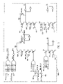
- FIG. 1 shows a circuit diagram utilizing a sense amplifier in accordance with an embodiment of the present invention.
- FIG. 2 shows an exemplary circuit for a portion of the circuit diagram of FIG. 1 in accordance with an embodiment of the present invention.
- FIG. 3 shows an exemplary circuit for a portion of the circuit diagram of FIG. 1 in accordance with an embodiment of the present invention.
- FIG. 4 shows a block diagram of a sense amplifier application in accordance with an embodiment of the present invention.
- FIG. 5 shows a circuit diagram for a portion of the block diagram of FIG. 4 in accordance with an embodiment of the present invention.
- FIG. 6 shows a state diagram for the circuit diagram of FIG. 5 in accordance with an embodiment of the present invention.
- FIG. 1 shows a circuit 100 in accordance with an embodiment of the present invention.
- Circuit 100 represents, for example, a portion of a memory array and illustrates certain aspects of the present invention.
- one or more of the techniques disclosed herein are applicable to a number of different types of sense amplifier applications, such as for example for sense amplifier applications within a product term circuit of a programmable logic device.
- Circuit 100 includes logic gates 102 , 104 , 106 , and 108 , precharge circuits 110 and 112 , a sense amplifier 114 , a latch 116 , pass gates 122 , and inverters 124 and 126 .
- a column select signal 128 and an enable signal 130 are asserted (e.g., a logical high level)
- logic gate 102 e.g., a NAND gate
- logic gate 104 switches off precharge circuit 112 and switches on sense amplifier 114 via an enable signal 138 to initiate a read operation of bitlines 118 and 120 by sense amplifier 114 .
- Precharge circuit 110 in general, is switched off at approximately the same time as when precharge circuit 112 is switched off to allow sense amplifier 114 to read the values on bitlines 118 and 120 from the selected memory cell (not shown). Precharge circuit 110 is switched on to precharge bitlines 118 and 120 (e.g., globally within the memory array of which circuit 100 forms a part of) after the completion of a read cycle (e.g., after all trip signals, such as a trip signal 134 described herein, are asserted and the selected word line for the read cycle has been deasserted). In general, bitlines 118 and 120 (e.g., globally and locally to sense amplifier 114 ) must be precharged prior to each read by sense amplifier 114 .
- Inverters 124 and 126 are coupled to bitlines 118 and 120 leading into sense amplifier 114 and, along with logic gate 106 (e.g., a NOR gate), form a read completion detection circuit.
- a trip signal 136 provided by logic gate 106 transitions to a logical low level (or its complement, a trip signal 134 , transitions to a logical high level) once a read operation is completed by sense amplifier 114 .
- Trip signal 136 remains at a logical low level until the precharging is completed by precharge circuit 112 of bitlines 118 and 120 (i.e., at the input to sense amplifier 114 ).
- Inverters 124 and 126 help to isolate sense amplifier 114 from large capacitive loads and to provide their outputs (labeled DOUTB and DOUT, respectively) to logic gate 106 .
- Inverters 124 and 126 are placed between bitlines 118 and 120 and logic gate 106 to reduce parasitic capacitances.
- a logic gate e.g., a NAND gate
- inverters 124 and 126 not implemented would typically have parasitic capacitances associated with its n-channel field effect transistors (NFETS) that couple to nodes with different potentials within the logic gate and, consequently would not present identical loads to bitlines 118 and 120 .
- NETS n-channel field effect transistors
- the output signal (labeled DOUT) from inverter 126 is also provided to latch 116 (e.g., a D flip flop), while trip signal 134 is utilized as a clock for latch 116 .
- Latch 116 may also receive a reset signal 132 (e.g., a global reset). Latch 116 stores the result of a read operation by sense amplifier 114 and provides the result as an output signal 140 .
- the precharge cycle for the next read operation can begin immediately.
- enable signal 130 may transition to a logical low level (e.g., deasserted), which results in logic gate 102 switching off pass gates 122 and logic gate 104 switching off sense amplifier 114 and switching on precharge circuit 112 to begin charging bitlines 118 and 120 locally at sense amplifier 114 .
- Precharge circuit 110 would begin precharging bitlines 118 and 120 globally within the memory array, for example, once all of the sense amplifiers within the memory array have completed their read operation and the selected word line has been deasserted.
- FIG. 2 shows a circuit 200 , which is an exemplary circuit implementation for sense amplifier 114 of FIG. 1 in accordance with an embodiment of the present invention.
- Circuit 200 includes two cross-coupled inverters whose connection to a reference voltage (e.g., ground) is opened when enable signal 138 is deasserted. Thus, when enable signal 138 is asserted, circuit 200 performs a read operation of bitlines 118 and 120 .
- a reference voltage e.g., ground
- FIG. 3 shows a circuit 300 , which is an exemplary circuit implementation for precharge circuit 112 of FIG. 1 in accordance with an embodiment of the present invention.
- Circuit 300 may also be an exemplary circuit implementation for precharge circuit 110 , but its control signal would generally differ (i.e., enable signal 138 would be replaced, such as by a control signal 142 labeled BL_PCHG_B in FIG. 1 ) and transistor sizes may differ (e.g., transistor sizes for precharge circuit 110 would increase relative to precharge circuit 112 ), depending upon the size of the memory array with precharge circuit 110 generally having to precharge a longer portion of bitlines 118 and 120 than precharge circuit 112 .
- circuit 100 includes a read completion detection circuit and a self-timed precharge circuit.
- circuit 100 detects when sense amplifier 114 has read a bit (also referred to as when sense amplifier 114 has tripped) on bitlines 118 and 120 (i.e., trip signal 136 transitions to a logical low level).
- Circuit 100 also detects when the inputs to sense amplifier 114 have completed their precharge cycle (i.e., when precharge circuit 112 has locally precharged bitlines 118 and 120 at sense amplifier 114 ) by monitoring trip signal 136 for a transition to a logical high level (or by monitoring its complement, trip signal 134 ).
- circuit 100 may be extended to select from a number of bitline pairs.
- column select signal 128 may represent complementary signals (as indicated by ⁇ 1:0> notation in FIG. 1 and by a similar notation for other elements in FIG. 1 ), with logic gate 102 representing two logic gates, pass gates 122 representing two pairs of pass gates, and bitlines 118 and 120 representing two pairs of bitlines.
- the two pairs of pass gates 122 form a column multiplexer, which is controlled to select which pair of bitlines to route to sense amplifier 114 .
- Precharge circuit 110 may also represent two precharge circuits, one for each pair of bitlines.
- Enable signal 130 would be fed to both logic gates represented by logic gate 102 , with one of the column select signals routed to one logic gate and the complement routed to the other logic gate.
- the description herein may reference certain figure elements (e.g., logic gate 102 , pass gates 122 , etc.) in a singular sense, but it should be understood that a number of these figure elements may be implemented, for example, to accommodate the selection of any number of bitline pairs to route to sense amplifier 114 in accordance with one or more embodiments of the present invention.
- More than one sense amplifier 114 may be controlled by a control circuit (e.g., a sense amplifier controller). For example, depending on the actual granularity (e.g., a bit, a nibble, or a word) of the sense amplifier controllers for sense amplifiers 114 within the memory array, this technique may reduce the read precharge cycle time by eliminating the signal propagation delays associated with large memory arrays.
- a control circuit e.g., a sense amplifier controller
- FIG. 4 shows a block diagram 400 for sense amplifier control in accordance with an embodiment of the present invention.
- a block 402 represents a sense amplifier controller, which provides an enable signal 414 to four sense amplifiers circuits (e.g., enable signal 414 corresponding to enable signal 130 is provided to control four of circuits 100 ) represented by a block 404 (i.e., block 404 represents four sense amplifier circuits, as indicated by the notation ⁇ 3:0>, with each sense amplifier circuit selecting between two pairs of bitlines).
- block 402 controls the reading of four bits (i.e., a granularity of a nibble).
- Block 402 receives a read enable signal 406 , a reset signal 408 , four trip signals 410 , and four trip signals 412 (corresponding complements of trip signals 410 ) and provides enable signal 414 to block 404 .
- Read enable signal 406 may be delayed appropriately so that sense amplifiers within block 404 are not enabled before their associated bitlines have started to separate in terms of their voltage.
- Reset signal 408 may be a global reset signal (e.g., the same signal as reset signal 132 of FIG. 1 ).
- Trip signals 410 and 412 provide true and complement trip signals from completion detection circuits within block 404 , whose operation is as described similarly in reference to FIG. 1 for trip signals 134 and 136 .
- Block 404 provides trip signals 410 and 412 , as discussed above, along with four output signals 416 and receives four control signals 418 , two column select signals 420 , reset signal 408 , and eight bitlines 422 and 424 .
- Output signals 416 provide the results from the four sense amplifiers as described similarly in reference to FIG. 1 for output signal 140 .
- control signals 418 , column select signals 420 , and bitlines 422 and 424 operate in a similar fashion as described similarly in reference to FIG. 1 for control signal 142 , column select signal 128 , and bitlines 118 and 120 , respectively.
- FIG. 5 shows a circuit 500 , which is an exemplary circuit implementation for block 402 of FIG. 4 in accordance with an embodiment of the present invention.
- FIG. 6 shows a state diagram 600 for circuit 500 of FIG. 5 in accordance with an embodiment of the present invention.
- the appropriate signal may be chosen from trip 1 , trip 2 , trip 3 , and trip 4 signals shown in FIG. 5 for state diagram 600 , based on whether all of the trip signals should be logically high or logically low for a desired state transition and on the polarity required.
- the signals listed to the left of the slash “/” indicate a transition or input, while the signals listed to the right of the slash “/” indicate a result of the transition or the input as a transition from one state to the next occurs.
- a transition from state zero to state three occurs if reset signal 408 is asserted, with a return to state zero when reset signal 408 is deasserted.
- enable signal 414 is asserted and a transition to state one occurs.
- the column pass gates are enabled, the precharge circuits are switched off, and the sense amplifiers are switched on.
- a transition to state two occurs (i.e., the trip signals from the monitored sense amplifiers are asserted)
- the sense amplifiers are switched off and the precharge of the bitlines begins again.
- the trip signals are deasserted and a transition to state six occurs followed by a transition to state zero when read enable signal 406 is deasserted.
- the trip signals from four adjacent bits may be fed to a single sense amplifier enable state machine.
- This level of granularity may accommodate various memory configurations of the memory array. Other levels of granularity, however, may be implemented based on one or more embodiments of the present invention and on the requirements of the desired application.
- one of the basic functions of the sense amplifier enable state machine is to appropriately assert the enable signal when a read enable input signal is asserted, and appropriately deassert the enable signal when all of the trip signals are asserted (as described herein).
- a new read address and the read enable signal are latched into their input registers by a read clock. While the read address is decoded and the correct wordline is enabled, the registered read enable signal is delayed by a similar amount of time so that the sense amplifier is not enabled before the bitlines have started to separate in terms of their voltage.
- the delayed read enable signal (e.g., read enable signal 406 ) is then received by a sense amplifier enable state machine (e.g., block 402 ), which enables a column multiplexer to connect the correct column bitlines to the local sense amplifier bitlines and terminates the precharge of the sense amplifier bitlines.
- the sense amplifier e.g., sense amplifier 114
- the read enable register is cleared, resulting in the registered read enable signal to go low.
- the trip signal will go low, signaling the sense amplifier enable state machine that the sense amplifier is ready for the next read cycle.
Landscapes
- Static Random-Access Memory (AREA)
- Dram (AREA)
- Amplifiers (AREA)
Abstract
Description
Claims (10)
Priority Applications (1)
| Application Number | Priority Date | Filing Date | Title |
|---|---|---|---|
| US11/435,956 US7102934B1 (en) | 2004-03-09 | 2006-05-17 | Sense amplifier systems and methods |
Applications Claiming Priority (2)
| Application Number | Priority Date | Filing Date | Title |
|---|---|---|---|
| US10/797,759 US7068556B2 (en) | 2004-03-09 | 2004-03-09 | Sense amplifier systems and methods |
| US11/435,956 US7102934B1 (en) | 2004-03-09 | 2006-05-17 | Sense amplifier systems and methods |
Related Parent Applications (1)
| Application Number | Title | Priority Date | Filing Date |
|---|---|---|---|
| US10/797,759 Division US7068556B2 (en) | 2004-03-09 | 2004-03-09 | Sense amplifier systems and methods |
Publications (2)
| Publication Number | Publication Date |
|---|---|
| US7102934B1 true US7102934B1 (en) | 2006-09-05 |
| US20060209608A1 US20060209608A1 (en) | 2006-09-21 |
Family
ID=34920114
Family Applications (2)
| Application Number | Title | Priority Date | Filing Date |
|---|---|---|---|
| US10/797,759 Active 2024-10-15 US7068556B2 (en) | 2004-03-09 | 2004-03-09 | Sense amplifier systems and methods |
| US11/435,956 Expired - Lifetime US7102934B1 (en) | 2004-03-09 | 2006-05-17 | Sense amplifier systems and methods |
Family Applications Before (1)
| Application Number | Title | Priority Date | Filing Date |
|---|---|---|---|
| US10/797,759 Active 2024-10-15 US7068556B2 (en) | 2004-03-09 | 2004-03-09 | Sense amplifier systems and methods |
Country Status (2)
| Country | Link |
|---|---|
| US (2) | US7068556B2 (en) |
| WO (1) | WO2005091934A2 (en) |
Cited By (2)
| Publication number | Priority date | Publication date | Assignee | Title |
|---|---|---|---|---|
| US8654600B1 (en) | 2011-03-01 | 2014-02-18 | Lattice Semiconductor Corporation | Low-voltage current sense amplifier |
| US20170178742A1 (en) * | 2015-12-18 | 2017-06-22 | Texas Instruments Incorporated | Self-Latch Sense Timing in a One-Time-Programmable Memory Architecture |
Families Citing this family (4)
| Publication number | Priority date | Publication date | Assignee | Title |
|---|---|---|---|---|
| US7477551B2 (en) * | 2006-11-08 | 2009-01-13 | Texas Instruments Incorporated | Systems and methods for reading data from a memory array |
| CN103178812B (en) * | 2011-12-26 | 2015-10-14 | 上海华虹宏力半导体制造有限公司 | A kind of clock synchronization read operation control signal generator |
| CN104575606B (en) * | 2013-10-10 | 2018-05-22 | 无锡华润上华科技有限公司 | A kind of reading circuit and control method with self-detection circuit |
| US11568948B2 (en) | 2021-02-12 | 2023-01-31 | Taiwan Semiconductor Manufacturing Company, Ltd. | Memory circuit and method of operating same |
Citations (15)
| Publication number | Priority date | Publication date | Assignee | Title |
|---|---|---|---|---|
| US4107556A (en) | 1977-05-12 | 1978-08-15 | Rca Corporation | Sense circuit employing complementary field effect transistors |
| US5361227A (en) * | 1991-12-19 | 1994-11-01 | Kabushiki Kaisha Toshiba | Non-volatile semiconductor memory device and memory system using the same |
| US5867443A (en) * | 1995-08-17 | 1999-02-02 | The United States Of America As Represented By The Secretary Of The Air Force | Shared bitline heterogeneous memory |
| US5973992A (en) | 1997-08-14 | 1999-10-26 | Micron Technology, Inc. | Tracking signals |
| US6072738A (en) | 1998-03-09 | 2000-06-06 | Lsi Logic Corporation | Cycle time reduction using an early precharge |
| US6195277B1 (en) | 1999-09-13 | 2001-02-27 | Lara Technology, Inc. | Multiple signal detection circuit |
| US6285583B1 (en) | 2000-02-17 | 2001-09-04 | Advanced Micro Devices, Inc. | High speed sensing to detect write protect state in a flash memory device |
| US6324110B1 (en) | 1999-03-12 | 2001-11-27 | Monolithic Systems Technology, Inc. | High-speed read-write circuitry for semi-conductor memory |
| US6418073B1 (en) | 1999-05-14 | 2002-07-09 | Nec Corporation | Semiconductor memory device |
| US6618313B2 (en) * | 2001-02-23 | 2003-09-09 | Intel Corporation | Self-timed activation logic for memory |
| US20040196686A1 (en) * | 2003-04-03 | 2004-10-07 | Kauffmann Brian R. | Static random access memory (sram) without precharge circuitry |
| US20060034121A1 (en) * | 2003-09-17 | 2006-02-16 | Shahzad Khalid | Non-volatile memory and method with bit line compensation dependent on neighboring operating modes |
| US20060034139A1 (en) * | 2004-08-11 | 2006-02-16 | Hynix Semiconductor Inc. | Semiconductor memory device |
| US20060087898A1 (en) * | 2004-10-22 | 2006-04-27 | Hynix Semiconductor Inc. | Leakage current control device of semiconductor memory device |
| US20060120184A1 (en) * | 2003-06-25 | 2006-06-08 | Samsung Electronics, Co., Ltd. | Sense amplifier driver and semiconductor device comprising the same |
-
2004
- 2004-03-09 US US10/797,759 patent/US7068556B2/en active Active
-
2005
- 2005-03-02 WO PCT/US2005/006716 patent/WO2005091934A2/en active Application Filing
-
2006
- 2006-05-17 US US11/435,956 patent/US7102934B1/en not_active Expired - Lifetime
Patent Citations (15)
| Publication number | Priority date | Publication date | Assignee | Title |
|---|---|---|---|---|
| US4107556A (en) | 1977-05-12 | 1978-08-15 | Rca Corporation | Sense circuit employing complementary field effect transistors |
| US5361227A (en) * | 1991-12-19 | 1994-11-01 | Kabushiki Kaisha Toshiba | Non-volatile semiconductor memory device and memory system using the same |
| US5867443A (en) * | 1995-08-17 | 1999-02-02 | The United States Of America As Represented By The Secretary Of The Air Force | Shared bitline heterogeneous memory |
| US5973992A (en) | 1997-08-14 | 1999-10-26 | Micron Technology, Inc. | Tracking signals |
| US6072738A (en) | 1998-03-09 | 2000-06-06 | Lsi Logic Corporation | Cycle time reduction using an early precharge |
| US6324110B1 (en) | 1999-03-12 | 2001-11-27 | Monolithic Systems Technology, Inc. | High-speed read-write circuitry for semi-conductor memory |
| US6418073B1 (en) | 1999-05-14 | 2002-07-09 | Nec Corporation | Semiconductor memory device |
| US6195277B1 (en) | 1999-09-13 | 2001-02-27 | Lara Technology, Inc. | Multiple signal detection circuit |
| US6285583B1 (en) | 2000-02-17 | 2001-09-04 | Advanced Micro Devices, Inc. | High speed sensing to detect write protect state in a flash memory device |
| US6618313B2 (en) * | 2001-02-23 | 2003-09-09 | Intel Corporation | Self-timed activation logic for memory |
| US20040196686A1 (en) * | 2003-04-03 | 2004-10-07 | Kauffmann Brian R. | Static random access memory (sram) without precharge circuitry |
| US20060120184A1 (en) * | 2003-06-25 | 2006-06-08 | Samsung Electronics, Co., Ltd. | Sense amplifier driver and semiconductor device comprising the same |
| US20060034121A1 (en) * | 2003-09-17 | 2006-02-16 | Shahzad Khalid | Non-volatile memory and method with bit line compensation dependent on neighboring operating modes |
| US20060034139A1 (en) * | 2004-08-11 | 2006-02-16 | Hynix Semiconductor Inc. | Semiconductor memory device |
| US20060087898A1 (en) * | 2004-10-22 | 2006-04-27 | Hynix Semiconductor Inc. | Leakage current control device of semiconductor memory device |
Cited By (4)
| Publication number | Priority date | Publication date | Assignee | Title |
|---|---|---|---|---|
| US8654600B1 (en) | 2011-03-01 | 2014-02-18 | Lattice Semiconductor Corporation | Low-voltage current sense amplifier |
| US20170178742A1 (en) * | 2015-12-18 | 2017-06-22 | Texas Instruments Incorporated | Self-Latch Sense Timing in a One-Time-Programmable Memory Architecture |
| US9881687B2 (en) * | 2015-12-18 | 2018-01-30 | Texas Instruments Incorporated | Self-latch sense timing in a one-time-programmable memory architecture |
| US10192629B2 (en) | 2015-12-18 | 2019-01-29 | Texas Instruments Incorporated | Self-latch sense timing in a one-time-programmable memory architecture |
Also Published As
| Publication number | Publication date |
|---|---|
| US7068556B2 (en) | 2006-06-27 |
| US20060209608A1 (en) | 2006-09-21 |
| WO2005091934A3 (en) | 2006-09-14 |
| US20050201172A1 (en) | 2005-09-15 |
| WO2005091934A2 (en) | 2005-10-06 |
Similar Documents
| Publication | Publication Date | Title |
|---|---|---|
| US5828610A (en) | Low power memory including selective precharge circuit | |
| EP0554489B1 (en) | Multi-port static random access memory with fast write-thru scheme | |
| US8422313B2 (en) | Reduced power consumption memory circuitry | |
| JP3221900B2 (en) | Semiconductor memory having precharge type redundant multiplex operation | |
| US6392957B1 (en) | Fast read/write cycle memory device having a self-timed read/write control circuit | |
| JPH04291093A (en) | Reading/writing memory provided with improved writing driver | |
| JPH04298892A (en) | Semiconductor memory having column balancing in data change during writing cycle period | |
| US5777935A (en) | Memory device with fast write recovery and related write recovery method | |
| KR20080046639A (en) | Memory with robust data sensing and method for sensing data | |
| CN107750380B (en) | High speed pseudo-dual port memory with split precharge control | |
| US7102934B1 (en) | Sense amplifier systems and methods | |
| US7483289B2 (en) | Synchronous SRAM capable of faster read-modify-write operation | |
| JP3754593B2 (en) | Integrated circuit having memory cells for storing data bits and method for writing write data bits to memory cells in integrated circuits | |
| US7355881B1 (en) | Memory array with global bitline domino read/write scheme | |
| US6058052A (en) | Redundancy scheme providing improvements in redundant circuit access time and integrated circuit layout area | |
| US7289373B1 (en) | High performance memory device | |
| US8325543B2 (en) | Global bit select circuit interface with false write through blocking | |
| US6249471B1 (en) | Fast full signal differential output path circuit for high-speed memory | |
| US7233542B2 (en) | Method and apparatus for address generation | |
| US6320794B1 (en) | Late-write type semiconductor memory device with multi-channel data output multiplexer | |
| JP2588936B2 (en) | Semiconductor storage device | |
| US6219285B1 (en) | Semiconductor storage device with synchronized selection of normal and redundant columns | |
| JPH0883491A (en) | Data read-out circuit | |
| JP3281034B2 (en) | Semiconductor storage device | |
| EP0685851B1 (en) | Control circuitry for shared data bus in a memory integrated circuit |
Legal Events
| Date | Code | Title | Description |
|---|---|---|---|
| FEPP | Fee payment procedure |
Free format text: PAYOR NUMBER ASSIGNED (ORIGINAL EVENT CODE: ASPN); ENTITY STATUS OF PATENT OWNER: LARGE ENTITY |
|
| AS | Assignment |
Owner name: LATTICE SEMICONDUCTRO CORPORATION, OREGON Free format text: ASSIGNMENT OF ASSIGNORS INTEREST;ASSIGNORS:CRUZ, LOUIS DE LA;WHITE, ALLEN;REEL/FRAME:017704/0530 Effective date: 20040308 |
|
| STCF | Information on status: patent grant |
Free format text: PATENTED CASE |
|
| FPAY | Fee payment |
Year of fee payment: 4 |
|
| FPAY | Fee payment |
Year of fee payment: 8 |
|
| AS | Assignment |
Owner name: JEFFERIES FINANCE LLC, NEW YORK Free format text: SECURITY INTEREST;ASSIGNORS:LATTICE SEMICONDUCTOR CORPORATION;SIBEAM, INC.;SILICON IMAGE, INC.;AND OTHERS;REEL/FRAME:035223/0001 Effective date: 20150310 |
|
| MAFP | Maintenance fee payment |
Free format text: PAYMENT OF MAINTENANCE FEE, 12TH YEAR, LARGE ENTITY (ORIGINAL EVENT CODE: M1553) Year of fee payment: 12 |
|
| AS | Assignment |
Owner name: DVDO, INC., OREGON Free format text: RELEASE BY SECURED PARTY;ASSIGNOR:JEFFERIES FINANCE LLC;REEL/FRAME:049827/0326 Effective date: 20190517 Owner name: SILICON IMAGE, INC., OREGON Free format text: RELEASE BY SECURED PARTY;ASSIGNOR:JEFFERIES FINANCE LLC;REEL/FRAME:049827/0326 Effective date: 20190517 Owner name: LATTICE SEMICONDUCTOR CORPORATION, OREGON Free format text: RELEASE BY SECURED PARTY;ASSIGNOR:JEFFERIES FINANCE LLC;REEL/FRAME:049827/0326 Effective date: 20190517 Owner name: SIBEAM, INC., OREGON Free format text: RELEASE BY SECURED PARTY;ASSIGNOR:JEFFERIES FINANCE LLC;REEL/FRAME:049827/0326 Effective date: 20190517 Owner name: WELLS FARGO BANK, NATIONAL ASSOCIATION, AS ADMINIS Free format text: SECURITY INTEREST;ASSIGNOR:LATTICE SEMICONDUCTOR CORPORATION;REEL/FRAME:049980/0786 Effective date: 20190517 Owner name: WELLS FARGO BANK, NATIONAL ASSOCIATION, AS ADMINISTRATIVE AGENT, COLORADO Free format text: SECURITY INTEREST;ASSIGNOR:LATTICE SEMICONDUCTOR CORPORATION;REEL/FRAME:049980/0786 Effective date: 20190517 |