US7038483B1 - System and method for measuring transistor leakage current with a ring oscillator - Google Patents
System and method for measuring transistor leakage current with a ring oscillator Download PDFInfo
- Publication number
- US7038483B1 US7038483B1 US11/070,630 US7063005A US7038483B1 US 7038483 B1 US7038483 B1 US 7038483B1 US 7063005 A US7063005 A US 7063005A US 7038483 B1 US7038483 B1 US 7038483B1
- Authority
- US
- United States
- Prior art keywords
- test
- leakage
- signal
- leakage current
- generation circuit
- Prior art date
- Legal status (The legal status is an assumption and is not a legal conclusion. Google has not performed a legal analysis and makes no representation as to the accuracy of the status listed.)
- Expired - Lifetime
Links
Images


Classifications
-
- G—PHYSICS
- G01—MEASURING; TESTING
- G01R—MEASURING ELECTRIC VARIABLES; MEASURING MAGNETIC VARIABLES
- G01R31/00—Arrangements for testing electric properties; Arrangements for locating electric faults; Arrangements for electrical testing characterised by what is being tested not provided for elsewhere
- G01R31/26—Testing of individual semiconductor devices
- G01R31/2607—Circuits therefor
- G01R31/2621—Circuits therefor for testing field effect transistors, i.e. FET's
-
- G—PHYSICS
- G01—MEASURING; TESTING
- G01R—MEASURING ELECTRIC VARIABLES; MEASURING MAGNETIC VARIABLES
- G01R31/00—Arrangements for testing electric properties; Arrangements for locating electric faults; Arrangements for electrical testing characterised by what is being tested not provided for elsewhere
- G01R31/50—Testing of electric apparatus, lines, cables or components for short-circuits, continuity, leakage current or incorrect line connections
- G01R31/52—Testing for short-circuits, leakage current or ground faults
-
- G—PHYSICS
- G01—MEASURING; TESTING
- G01R—MEASURING ELECTRIC VARIABLES; MEASURING MAGNETIC VARIABLES
- G01R31/00—Arrangements for testing electric properties; Arrangements for locating electric faults; Arrangements for electrical testing characterised by what is being tested not provided for elsewhere
- G01R31/26—Testing of individual semiconductor devices
- G01R31/27—Testing of devices without physical removal from the circuit of which they form part, e.g. compensating for effects surrounding elements
-
- G—PHYSICS
- G01—MEASURING; TESTING
- G01R—MEASURING ELECTRIC VARIABLES; MEASURING MAGNETIC VARIABLES
- G01R31/00—Arrangements for testing electric properties; Arrangements for locating electric faults; Arrangements for electrical testing characterised by what is being tested not provided for elsewhere
- G01R31/28—Testing of electronic circuits, e.g. by signal tracer
- G01R31/2851—Testing of integrated circuits [IC]
- G01R31/2884—Testing of integrated circuits [IC] using dedicated test connectors, test elements or test circuits on the IC under test
Definitions
- Embodiments of the present invention relate to the field of semi-conductor circuits. More specifically, embodiments of the present invention relate to the field of ring oscillators for measuring characteristics of a semi-conductor device.
- the power dissipated by a digital chip has two basic sources which are switching current and leakage current.
- switching current When a gate is switching from one logical value to another, there is a brief period time where current passes through the transistors dissipating power in the form of heat. Historically, this switching current has been the focus of the designer's attention because it was substantially greater than the nominal leakage current that occurred when the gate was not switching and the transistors were “off”.
- the leakage current is a significantly larger proportion of the power production problem.
- chip designers need to develop both on and off chip techniques for dealing with leakage current.
- One of the challenges is accurately measuring the amount of leakage current that is actually present on a particular chip.
- Embodiments of the present invention are directed toward a system and method for accurately measuring the leakage current of one or more transistors on a chip. Specifically, a ring oscillator with a frequency directly related to the leakage current is described herein.
- a signal generation circuit has a dynamic node driver with a pre-charge device and a leakage test device that is biased to an off state, a differential amplifier coupled to the dynamic node driver and to a delay unit.
- the delay unit drives the pre-charge device.
- a signal generation circuit is described with a pre-charge device and a leakage test device that may be biased to an off state forming a dynamic node driver.
- the dynamic node driver drives a test delay unit that may drive the pre-charge device.
- a signal generation circuit comprising a test oscillator with a dynamic node driver and a test loop delay and are reference oscillator with a reference loop delay.
- the dynamic node driver has a leakage test device that is biased to an off state.
- the reference loop delay can be comparable to the test loop delay.
- a method of generating a signal with a frequency related to leakage current involves driving a ring oscillator with a dynamic node driver.
- the dynamic node driver may have a pre-charge device and a leakage test device biased to an off state.
- a method of measuring the leakage current involves driving a ring oscillator with a dynamic node driver having a leakage test device biased to an off state to produce a test signal.
- the test signal is extracted and the frequency is measured.
- the leakage current is estimated from the measured frequency.
- FIG. 1 is a block diagram of a leakage current measurement system in accordance with an embodiment of the present invention.
- FIG. 2 is a block diagram of a signal measurement unit in accordance with an embodiment of the present invention.
- FIG. 3 is a schematic for an exemplary ring oscillator having a fundamental frequency proportional to the leakage current in a device under test in accordance with an embodiment of the present invention.
- FIG. 4 is an example of a signal at the dynamic node in the schematic of FIG. 3 in accordance with an embodiment of the present invention.
- FIG. 5 is an example of a signal after processing by a differential amplifier in accordance with an embodiment of the present invention.
- FIG. 6 is an example of a signal after passing through a flip-flop in accordance with an embodiment of the present invention.
- FIG. 7 is a block diagram of an exemplary leakage current measurement system using a reference circuit in accordance with an embodiment of the present invention.
- FIG. 8 is a schematic of an exemplary reference circuit in accordance with an embodiment of the present invention.
- FIG. 9 is a block diagram of a leakage current measurement system that provides for multiplexing gates to use the same differential amplifier and delay unit for both reference and test measurements.
- FIG. 10 is a schematic of an exemplary ring oscillator supporting a test and reference mode.
- FIG. 11 is an NMOS transistor configured for use as a device under test to measure the transistor leakage current in accordance with an embodiment of the present invention.
- FIG. 12 is a PMOS transistor configured for use as a device under test to measure the transistor leakage current in accordance with an embodiment of the present invention.
- FIG. 13 is an NMOS transistor configured for use as a device under test to measure the gate leakage current in accordance with an embodiment of the present invention.
- FIG. 14 is a PMOS transistor configured for use as a device under test to measure the gate leakage current in accordance with an embodiment of the present invention.
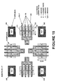
- FIG. 15 is the layout of four NMOS transistors implementing the schematic of FIG. 11 in accordance with an embodiment of the present invention.
- FIG. 16 is the layout of four PMOS transistors implementing the schematic of FIG. 12 in accordance with an embodiment of the present invention.
- FIG. 17 is the layout of four NMOS transistors implementing the schematic of FIG. 13 in accordance with an embodiment of the present invention.
- FIG. 18 is the layout of four PMOS transistors implementing the schematic of FIG. 14 in accordance with an embodiment of the present invention.
- FIG. 1 shows a block diagram of an exemplary embodiment of the present invention.
- One exemplary structure is a ring oscillator composed of a pre-charge device 100 , a leakage test device 105 , a differential amplifier 110 , and a delay unit 120 .
- the leakage test device 105 is also known as the device under test (DUT). It is biased to the off-state.
- the leakage test device 105 and the pre-charge device together form a dynamic node driver.
- the pre-charge device 100 When the pre-charge device 100 is turned on, it brings the dynamic node 109 up to voltage V dd .
- the leakage test device 105 lets the charge accumulated at the dynamic node 109 bleed off.
- the resulting ring oscillator generates a periodic signal with a frequency that is directly related to the leakage current—a high leakage current results in a high frequency while a low leakage current results in a relatively low frequency.
- the delay unit 120 in combination with the differential amplifier 110 and the pre-charge device 100 must present an odd number of inversions around the loop.
- the periodic signal is tapped at test signal node 132 .
- the test signal measurement unit 130 conditions the test signal at the test signal node 132 by running it through one or more flip-flops (or comparable numbers of latches) as well as measuring the fundamental frequency of the test signal.
- the leakage current estimation unit 170 performs a calculation on the measured frequency to estimate the leakage current in the leakage test device 105 .
- FIG. 2 shows an exemplary embodiment of the test signal measurement unit 130 .
- the signal is conditioned by running through a divider 133 having one or more flip-flops (or comparable numbers of latches).
- the divider 133 serves to convert the test signal from a pulse to a waveform with a 50% duty cycle.
- the divider serves to divide the frequency of test signal to a suitable level for the counter 135 .
- the signal produced by the divider 133 increments counter 135 .
- the counter 135 has a reset 136 that is strobed with a periodic timing signal generated from a system clock or other stable and well-defined timing signal.
- the counter value 138 thus represents the number of cycles in the test signal in the time of one period of the periodic timing signal.
- the counter value 138 is thus proportional to the frequency of the test signal.
- FIG. 3 shows a schematic of an exemplary embodiment of the present invention.
- the pre-charge device 100 is a PMOS device and the leakage test device 105 is an NMOS device configured to measure transistor leakage current.
- the differential amplifier 110 compares the voltage of the dynamic node 109 with a reference voltage 108 (Vref). In one embodiment, V ref is taken to be one half of V dd .
- the differential amplifier produces a signal at differential node 111 .
- the delay unit in this embodiment is composed of a sequence of inverters 121 . If desired, additional delay can be placed in supplemental delay unit 122 .
- the delay unit in this embodiment also includes an enabling gate 123 with an enable input 127 .
- the enable input 127 can be used to stop the ring oscillator shown from operating.
- the flip-flop 134 is part of the divider 133 .
- FIGS. 4 , 5 and 6 illustrate the operation of an embodiment of the present invention by showing waveforms at various nodes in the circuit as a function of time.
- FIG. 4 shows the voltage at the dynamic node 109 .
- FIG. 5 shows that the result of the differential amplifier comparing the dynamic node 109 voltage to the reference voltage 108 , V ref .
- the ring oscillator is initialized by setting the enable input 127 to a low value. This prevents oscillation and yet turns the pre-charge device 100 on. This drives the dynamic node 109 to a high value.
- the enable input goes to a high value, the pre-charge device 100 is turned off.
- the dynamic node 109 is initially at greater value than V ref
- the differential amplifier and the delay elements with the appropriate number of inverters thus initially keeps the pre-charge device 100 turned off.
- the leakage test device 10 S is biased to the off-state, it does have a leakage current that bleeds off the charge at the dynamic node 109 until the dynamic node 109 voltage reaches V ref .
- FIG. 6 shows the result of having cleaned up the test signal by running it through a flip-flop.
- the average leakage current (per unit length) of a test leakage device 105 configured for transistor leakage current can be estimated with the following relationship:
- the average leakage current (per unit area) of a test leakage device 105 configured for gate leakage current can be estimated with the following relationship:
- I off C ⁇ ( V dd - V ref ) ⁇ 2 n ⁇ f t L ⁇ W
- the differential amplifier could be replaced with one or more inverters.
- the test signal can be obtained from any point within the ring oscillator. The total delay around the loop should be sufficient to permit the proper operation of test signal measurement unit 130 .
- FIG. 7 shows a system block diagram of an embodiment of the present invention to measure the leakage current in that situation.
- FIG. 7 shows a reference ring oscillator having a reference differential amplifier 140 and a reference delay unit 150 .
- the ring oscillator produces a reference signal with a fundamental frequency that is measured by the reference signal measurement unit 160 .
- the reference signal measurement unit 160 can have a similar structure to the test signal measurement unit 130 .
- the leakage current estimation unit 170 uses information about the test signal and the reference signal to compute an improved estimate of the leakage current.
- FIG. 8 shows a schematic of an embodiment of the reference oscillator in FIG. 7 .
- the reference differential amplifier 210 compares the voltage of the reference node 209 with a reference voltage 208 (Vref). In one embodiment, Vref is taken to be one half of V dd .
- the differential amplifier produces a signal at differential node 211 .
- the delay unit in this embodiment is composed of a sequence of inverters 221 . If desired, additional delay can be placed in supplemental delay unit 222 .
- the delay unit in this embodiment also includes an enabling gate 223 with an enable input 227 .
- the enable input 227 can be used to stop the reference oscillator shown from operating.
- the flip-flop 234 is part of the reference signal measurement unit 160 . The components of the reference oscillator should be adjusted and selected to produce a delay around the loop that is comparable to the delay found in the test differential amplifier 110 and test delay unit 120 .
- FIG. 9 shows a block diagram of an embodiment of the present invention that allows the reference oscillator and the test oscillator to share the differential amplifier and most of the delay unit.
- the components are the same as in the embodiment shown in FIG. 1 with the addition of isolation gate 107 and bypass gate 108 .
- at least one inverter 145 should be extracted from the delay unit 120 and placed after the connection to the bypass gate 108 .
- the isolation gate 107 is activated and the bypass gate is deactivated.
- the signal measurement unit 230 measures the frequency of the test signal.
- the isolation gate 107 is deactivated and the bypass gate 108 is activated, thus isolating the leakage test device 105 .
- the signal measurement unit 230 measures the frequency of the reference signal.
- the leakage current estimation unit 270 estimates the leakage current with two time-separated measurements made by the signal measurement unit 230 with the ring oscillator in different modes.
- FIG. 10 is a schematic illustrating the use of a common differential amplifier 110 and delay unit 120 to generate both a reference signal and a test signal.
- the isolation gate 107 is implemented as a pass gate 147 .
- the bypass gate is implemented as another pass gate 148 .
- a test mode signal 190 and the test mode signal negation 141 control the pass gates. To make effective measurements the transistors forming the pass gates 147 , 148 should be significantly smaller than the leakage test device 105 .
- the average leakage current (per unit length) of a test leakage device 105 configured for transistor leakage current can be estimated with the following relationship:
- the average leakage current (per unit area) of a test leakage device 105 configured for gate leakage current can be estimated with the following relationship:
- FIG. 11 shows a schematic for an NMOS leakage test device configured for measuring transistor leakage current.
- FIG. 12 shows a schematic for a PMOS leakage test device configured for measuring transistor leakage current.
- FIG. 13 shows a schematic for an NMOS leakage test device configured for measuring the gate leakage current.
- FIG. 14 shows a schematic for a PMOS leakage test device configured for measuring gate leakage current.
- FIG. 15 shows an embodiment of a layout of several NMOS transistors orthogonally arranged implementing the schematic of FIG. 11 .
- Four multi-fingered (or folded) transistors are shown. Each transistor is on top of the P substrate.
- Each transistor comprises an N-diffusion region 310 and a gate 315 formed with one or more gate fingers formed with polysilicon.
- the drain 320 and the source 321 are the alternating sub-regions of the N-diffusion region 310 .
- drain 320 is electrically connected to dynamic node 109 .
- the source 321 and the gate 315 are electrically connected to ground.
- the P-diffusion tap 305 is also connected to ground.
- source 321 is connected to dynamic node 109 and drain 320 is connected to ground.
- the effective width of the entire leakage test device is the number of gate fingers times the individual device width 330 .
- FIG. 16 shows an embodiment of a layout of several PMOS transistors orthogonally arranged implementing the schematic of FIG. 12 .
- Four multi-fingered (or folded) transistors are shown. Each transistor is on top of an N-well 350 formed in a P substrate.
- Each transistor comprises a P-diffusion region 360 and a gate 365 formed with one or more gate fingers formed with polysilicon.
- the drain 371 and the source 370 are the alternating sub-regions of the P-diffusion region 360 .
- drain 371 is connected to ground while the source 370 , the gate 365 and the N-diffusion tap 355 are connected to the dynamic node 109 .
- drain 371 is connected to the dynamic node 109 while the source 370 is connected to ground.
- the effective width of the entire leakage test device is the number of gate fingers times the individual device width 380 .
- FIG. 17 shows an embodiment of a layout of several transistors orthogonally arranged implementing the schematic of FIG. 13 .
- Four multi-fingered (or folded) transistors are shown.
- Each transistor is on top of the P substrate.
- Each transistor comprises an N-diffusion region 310 and a gate 315 formed with one or more gate fingers formed with polysilicon.
- the drain 320 and the source 321 are the alternating sub-regions of the N-diffusion region 310 .
- the gate 315 is electrically connected to dynamic node 109 and the drain 320 , the source 321 and the P-diffusion tap 305 are electrically connected to ground.
- the effective width of the entire leakage test device is the number of gate fingers times the individual device width 330 .
- the effective length of the transistor is the individual gate length 335 .
- FIG. 18 shows an embodiment of a layout of several transistors orthogonally arranged implementing the schematic of FIG. 14 .
- Four multi-fingered (or folded) transistors are shown.
- Each transistor is on top of an N-well 350 formed in a P substrate.
- Each transistor comprises a P-diffusion region 360 and a gate 365 formed with one more gate fingers formed with polysilicon.
- the drain 371 and the source 370 are the alternating sub-regions of the P-diffusion region 360 .
- the drain 371 , the source 370 and the N-diffusion tap 355 are connected to the dynamic node 109 while the gate 365 is connected to ground.
- the effective width of the entire leakage test device is the number of gate fingers times the individual device width 380 .
- the effective length of the transistor is the individual gate length 385 .
- the present invention a system and method for measuring leakage current have thus been disclosed. Using the present invention, an accurate estimate of the leakage current associated with a particular circuit device on a particular chip is obtained. While the present invention has been described in particular embodiments, it should be appreciated that the present invention should not be construed as limited by such embodiments, but rather construed according to the below claims.
Abstract
Description
-
- where n is the number of flip-flops before initiating counting in the test
signal measurement unit 130, W is the effective width of the test leakage device, C is the capacitance of thedynamic node 109, Vdd is the supply voltage, Vref is the reference voltage used in the differential amplifier, and ft is the frequency measured by the testsignal measurement unit 130.
- where n is the number of flip-flops before initiating counting in the test
-
- where n is the number of flip-flops before initiating counting in the test
signal measurement unit 130, W is the effective width of thetest leakage device 105, L is the effective length of the test leakage device, C is the capacitance of thedynamic node 109, Vdd is the supply voltage, Vref is the reference voltage used in the differential amplifier, and ft is the frequency of the test signal measured by the testsignal measurement unit 130.
- where n is the number of flip-flops before initiating counting in the test
-
- where n is the number of flip-flops before initiating counting in the test
signal measurement unit 130, W is the effective width of the test leakage device, C is the capacitance of thedynamic node 109, Vdd is the supply voltage, Vref is the reference voltage used in the differential amplifier, ft is the frequency measured by the testsignal measurement unit 130, and fr is the frequency measured by the reference signal measurement unit 160.
- where n is the number of flip-flops before initiating counting in the test
-
- where n is the number of flip-flops before initiating counting in the test
signal measurement unit 130, W is the effective width of thetest leakage device 105, L is the effective length of the test leakage device, C is the capacitance of thedynamic node 109, Vdd is the supply voltage, Vref is the reference voltage used in the differential amplifier, ft is the frequency of the test signal measured by the testsignal measurement unit 130, and fr is the frequency measured by the reference signal measurement unit 160.
- where n is the number of flip-flops before initiating counting in the test
Claims (19)
Priority Applications (1)
| Application Number | Priority Date | Filing Date | Title |
|---|---|---|---|
| US11/070,630 US7038483B1 (en) | 2002-04-16 | 2005-03-01 | System and method for measuring transistor leakage current with a ring oscillator |
Applications Claiming Priority (2)
| Application Number | Priority Date | Filing Date | Title |
|---|---|---|---|
| US10/124,152 US6882172B1 (en) | 2002-04-16 | 2002-04-16 | System and method for measuring transistor leakage current with a ring oscillator |
| US11/070,630 US7038483B1 (en) | 2002-04-16 | 2005-03-01 | System and method for measuring transistor leakage current with a ring oscillator |
Related Parent Applications (1)
| Application Number | Title | Priority Date | Filing Date |
|---|---|---|---|
| US10/124,152 Division US6882172B1 (en) | 2002-04-16 | 2002-04-16 | System and method for measuring transistor leakage current with a ring oscillator |
Publications (1)
| Publication Number | Publication Date |
|---|---|
| US7038483B1 true US7038483B1 (en) | 2006-05-02 |
Family
ID=34434256
Family Applications (3)
| Application Number | Title | Priority Date | Filing Date |
|---|---|---|---|
| US10/124,152 Expired - Lifetime US6882172B1 (en) | 2002-04-16 | 2002-04-16 | System and method for measuring transistor leakage current with a ring oscillator |
| US10/672,793 Expired - Lifetime US6885210B1 (en) | 2002-04-16 | 2003-09-26 | System and method for measuring transistor leakage current with a ring oscillator with backbias controls |
| US11/070,630 Expired - Lifetime US7038483B1 (en) | 2002-04-16 | 2005-03-01 | System and method for measuring transistor leakage current with a ring oscillator |
Family Applications Before (2)
| Application Number | Title | Priority Date | Filing Date |
|---|---|---|---|
| US10/124,152 Expired - Lifetime US6882172B1 (en) | 2002-04-16 | 2002-04-16 | System and method for measuring transistor leakage current with a ring oscillator |
| US10/672,793 Expired - Lifetime US6885210B1 (en) | 2002-04-16 | 2003-09-26 | System and method for measuring transistor leakage current with a ring oscillator with backbias controls |
Country Status (1)
| Country | Link |
|---|---|
| US (3) | US6882172B1 (en) |
Cited By (25)
| Publication number | Priority date | Publication date | Assignee | Title |
|---|---|---|---|---|
| US20070109006A1 (en) * | 2005-11-17 | 2007-05-17 | P.A. Semi, Inc. | Digital leakage detector |
| US7642866B1 (en) | 2005-12-30 | 2010-01-05 | Robert Masleid | Circuits, systems and methods relating to a dynamic dual domino ring oscillator |
| US7768356B2 (en) | 2005-12-30 | 2010-08-03 | Robert P Masleid | Dynamic ring oscillators |
| US7889014B1 (en) | 2004-11-04 | 2011-02-15 | Stoiber Steven T | Ring based impedance control of an output driver |
| US8942932B2 (en) | 2010-08-31 | 2015-01-27 | Advanced Micro Devices, Inc. | Determining transistor leakage for an integrated circuit |
| US9602083B2 (en) | 2013-07-03 | 2017-03-21 | Nvidia Corporation | Clock generation circuit that tracks critical path across process, voltage and temperature variation |
| US9766649B2 (en) | 2013-07-22 | 2017-09-19 | Nvidia Corporation | Closed loop dynamic voltage and frequency scaling |
| US9939883B2 (en) | 2012-12-27 | 2018-04-10 | Nvidia Corporation | Supply-voltage control for device power management |
| US10103719B2 (en) | 2013-07-22 | 2018-10-16 | Nvidia Corporation | Integrated voltage regulator with in-built process, temperature and aging compensation |
| CN109709465A (en) * | 2019-01-02 | 2019-05-03 | 电子科技大学 | A kind of MOSFET leakage current extraction circuit |
| US10473716B2 (en) | 2017-06-07 | 2019-11-12 | Samsung Electronics Co., Ltd. | Leakage current measurement circuit, integrated circuit and system including same |
| WO2021019539A1 (en) * | 2019-07-29 | 2021-02-04 | Proteantecs Ltd. | On-die thermal sensing network for integrated circuits |
| US11132485B2 (en) | 2018-06-19 | 2021-09-28 | Proteantecs Ltd. | Efficient integrated circuit simulation and testing |
| US11275700B2 (en) | 2018-12-30 | 2022-03-15 | Proteantecs Ltd. | Integrated circuit I/O integrity and degradation monitoring |
| US11293977B2 (en) | 2020-04-20 | 2022-04-05 | Proteantecs Ltd. | Die-to-die connectivity monitoring |
| US11313900B2 (en) | 2020-08-24 | 2022-04-26 | Stmicroelectronics International N.V. | Methods and devices for measuring leakage current |
| US11385282B2 (en) | 2017-11-15 | 2022-07-12 | Proteantecs Ltd. | Integrated circuit margin measurement and failure prediction device |
| US11391771B2 (en) | 2017-11-23 | 2022-07-19 | Proteantecs Ltd. | Integrated circuit pad failure detection |
| US11408932B2 (en) | 2018-01-08 | 2022-08-09 | Proteantecs Ltd. | Integrated circuit workload, temperature and/or subthreshold leakage sensor |
| US20220268857A1 (en) * | 2021-02-12 | 2022-08-25 | Nordic Semiconductor Asa | Power leakage testing |
| US11619551B1 (en) | 2022-01-27 | 2023-04-04 | Proteantecs Ltd. | Thermal sensor for integrated circuit |
| US11740281B2 (en) | 2018-01-08 | 2023-08-29 | Proteantecs Ltd. | Integrated circuit degradation estimation and time-of-failure prediction using workload and margin sensing |
| US11762013B2 (en) | 2018-04-16 | 2023-09-19 | Proteantecs Ltd. | Integrated circuit profiling and anomaly detection |
| US11815551B1 (en) | 2022-06-07 | 2023-11-14 | Proteantecs Ltd. | Die-to-die connectivity monitoring using a clocked receiver |
| US11929131B2 (en) | 2019-12-04 | 2024-03-12 | Proteantecs Ltd. | Memory device degradation monitoring |
Families Citing this family (64)
| Publication number | Priority date | Publication date | Assignee | Title |
|---|---|---|---|---|
| US7315178B1 (en) * | 2002-04-16 | 2008-01-01 | Transmeta Corporation | System and method for measuring negative bias thermal instability with a ring oscillator |
| US6882172B1 (en) * | 2002-04-16 | 2005-04-19 | Transmeta Corporation | System and method for measuring transistor leakage current with a ring oscillator |
| US7336090B1 (en) | 2002-04-16 | 2008-02-26 | Transmeta Corporation | Frequency specific closed loop feedback control of integrated circuits |
| US7941675B2 (en) * | 2002-12-31 | 2011-05-10 | Burr James B | Adaptive power control |
| US7212022B2 (en) * | 2002-04-16 | 2007-05-01 | Transmeta Corporation | System and method for measuring time dependent dielectric breakdown with a ring oscillator |
| US7112978B1 (en) | 2002-04-16 | 2006-09-26 | Transmeta Corporation | Frequency specific closed loop feedback control of integrated circuits |
| US7953990B2 (en) | 2002-12-31 | 2011-05-31 | Stewart Thomas E | Adaptive power control based on post package characterization of integrated circuits |
| US7949864B1 (en) | 2002-12-31 | 2011-05-24 | Vjekoslav Svilan | Balanced adaptive body bias control |
| US7228242B2 (en) | 2002-12-31 | 2007-06-05 | Transmeta Corporation | Adaptive power control based on pre package characterization of integrated circuits |
| US7109734B2 (en) * | 2003-12-18 | 2006-09-19 | Xilinx, Inc. | Characterizing circuit performance by separating device and interconnect impact on signal delay |
| US7692477B1 (en) | 2003-12-23 | 2010-04-06 | Tien-Min Chen | Precise control component for a substrate potential regulation circuit |
| US7649402B1 (en) | 2003-12-23 | 2010-01-19 | Tien-Min Chen | Feedback-controlled body-bias voltage source |
| US7129771B1 (en) | 2003-12-23 | 2006-10-31 | Transmeta Corporation | Servo loop for well bias voltage source |
| US7012461B1 (en) | 2003-12-23 | 2006-03-14 | Transmeta Corporation | Stabilization component for a substrate potential regulation circuit |
| US7336103B1 (en) | 2004-06-08 | 2008-02-26 | Transmeta Corporation | Stacked inverter delay chain |
| US7498846B1 (en) | 2004-06-08 | 2009-03-03 | Transmeta Corporation | Power efficient multiplexer |
| US7142018B2 (en) | 2004-06-08 | 2006-11-28 | Transmeta Corporation | Circuits and methods for detecting and assisting wire transitions |
| US7405597B1 (en) | 2005-06-30 | 2008-07-29 | Transmeta Corporation | Advanced repeater with duty cycle adjustment |
| US7304503B2 (en) | 2004-06-08 | 2007-12-04 | Transmeta Corporation | Repeater circuit with high performance repeater mode and normal repeater mode, wherein high performance repeater mode has fast reset capability |
| US7071747B1 (en) | 2004-06-15 | 2006-07-04 | Transmeta Corporation | Inverting zipper repeater circuit |
| US7774625B1 (en) | 2004-06-22 | 2010-08-10 | Eric Chien-Li Sheng | Adaptive voltage control by accessing information stored within and specific to a microprocessor |
| US7562233B1 (en) | 2004-06-22 | 2009-07-14 | Transmeta Corporation | Adaptive control of operating and body bias voltages |
| US7313779B1 (en) | 2004-10-12 | 2007-12-25 | Transmeta Corporation | Method and system for tiling a bias design to facilitate efficient design rule checking |
| US7205805B1 (en) | 2004-11-02 | 2007-04-17 | Western Digital Technologies, Inc. | Adjusting power consumption of digital circuitry relative to critical path circuit having the largest propagation delay error |
| US7788508B1 (en) | 2005-05-26 | 2010-08-31 | National Semiconductor Corporation | System and method for rapidly increasing a rising slew rate of an adjustable supply voltage in adaptive voltage scaling |
| US20070013425A1 (en) * | 2005-06-30 | 2007-01-18 | Burr James B | Lower minimum retention voltage storage elements |
| US7663408B2 (en) | 2005-06-30 | 2010-02-16 | Robert Paul Masleid | Scannable dynamic circuit latch |
| US7394681B1 (en) | 2005-11-14 | 2008-07-01 | Transmeta Corporation | Column select multiplexer circuit for a domino random access memory array |
| US7486060B1 (en) | 2006-03-30 | 2009-02-03 | Western Digital Technologies, Inc. | Switching voltage regulator comprising a cycle comparator for dynamic voltage scaling |
| US7551383B1 (en) | 2006-06-28 | 2009-06-23 | Western Digital Technologies, Inc. | Adjusting voltage delivered to disk drive circuitry based on a selected zone |
| US7710153B1 (en) | 2006-06-30 | 2010-05-04 | Masleid Robert P | Cross point switch |
| US7495466B1 (en) * | 2006-06-30 | 2009-02-24 | Transmeta Corporation | Triple latch flip flop system and method |
| US7330019B1 (en) | 2006-10-31 | 2008-02-12 | Western Digital Technologies, Inc. | Adjusting on-time for a discontinuous switching voltage regulator |
| WO2008129625A1 (en) * | 2007-04-10 | 2008-10-30 | Fujitsu Microelectronics Limited | Leak current detector circuit, body bias control circuit, semiconductor device, and semiconductor device testing method |
| ES2291143B2 (en) * | 2007-07-27 | 2008-07-16 | Universidad Politecnica De Madrid | DEVICE FOR MEASURING TEMPERATURE AND LEAK CURRENT IN A CHIP. |
| US7733189B1 (en) | 2007-09-14 | 2010-06-08 | Western Digital Technologies, Inc. | Oscillator comprising foldover detection |
| US7921312B1 (en) | 2007-09-14 | 2011-04-05 | National Semiconductor Corporation | System and method for providing adaptive voltage scaling with multiple clock domains inside a single voltage domain |
| US8085020B1 (en) | 2008-06-13 | 2011-12-27 | Western Digital Technologies, Inc. | Switching voltage regulator employing dynamic voltage scaling with hysteretic comparator |
| JP4693880B2 (en) * | 2008-08-12 | 2011-06-01 | 株式会社東芝 | Semiconductor integrated circuit |
| US8330478B2 (en) * | 2009-11-03 | 2012-12-11 | Arm Limited | Operating parameter monitoring circuit and method |
| US8154353B2 (en) * | 2009-11-03 | 2012-04-10 | Arm Limited | Operating parameter monitor for an integrated circuit |
| US8937404B1 (en) | 2010-08-23 | 2015-01-20 | Western Digital Technologies, Inc. | Data storage device comprising dual mode independent/parallel voltage regulators |
| US9425772B2 (en) | 2011-07-27 | 2016-08-23 | Nvidia Corporation | Coupling resistance and capacitance analysis systems and methods |
| US9496853B2 (en) | 2011-07-22 | 2016-11-15 | Nvidia Corporation | Via resistance analysis systems and methods |
| US8860817B2 (en) | 2011-07-25 | 2014-10-14 | Aptina Imaging Corporation | Imaging systems with verification circuitry for monitoring standby leakage current levels |
| US8952705B2 (en) | 2011-11-01 | 2015-02-10 | Nvidia Corporation | System and method for examining asymetric operations |
| US9448125B2 (en) | 2011-11-01 | 2016-09-20 | Nvidia Corporation | Determining on-chip voltage and temperature |
| CN103983809A (en) | 2013-02-08 | 2014-08-13 | 辉达公司 | PCB and online testing structure thereof, and manufacturing method of online testing structure |
| FR3014266B1 (en) * | 2013-12-03 | 2017-07-21 | Stmicroelectronics Rousset | METHOD AND DEVICE FOR CONTROLLING A BLOCKER SAMPLE. |
| CN105162419B (en) * | 2015-07-01 | 2017-11-17 | 东南大学 | Silicon substrate low-leakage current clamped beam grid metal-oxide-semiconductor cross coupled oscillator and preparation method |
| CN104967407B (en) * | 2015-07-01 | 2017-11-14 | 东南大学 | Gallium nitride base low-leakage current cantilever switch cross coupled oscillator and preparation method |
| CN105141261B (en) * | 2015-07-01 | 2017-11-17 | 东南大学 | Silicon substrate low-leakage current cantilever beam grid field effect transistor difference amplifier |
| CN104935252B (en) * | 2015-07-01 | 2018-01-16 | 东南大学 | The ring oscillator and preparation method of silicon substrate low-leakage current clamped beam grid |
| CN104993792B (en) * | 2015-07-01 | 2017-10-13 | 东南大学 | Gallium nitride base low-leakage current clamped beam switch cross coupled oscillator and preparation method |
| US10191108B2 (en) | 2015-11-19 | 2019-01-29 | Globalfoundries Inc. | On-chip sensor for monitoring active circuits on integrated circuit (IC) chips |
| US9863994B2 (en) | 2016-03-03 | 2018-01-09 | International Business Machines Corporation | On-chip leakage measurement |
| US10746785B2 (en) | 2016-08-05 | 2020-08-18 | International Business Machines Corporation | Dynamic predictor of semiconductor lifetime limits |
| US10394471B2 (en) | 2016-08-24 | 2019-08-27 | Qualcomm Incorporated | Adaptive power regulation methods and systems |
| US10365702B2 (en) | 2017-04-10 | 2019-07-30 | International Business Machines Corporation | Autonomic supply voltage compensation for degradation of circuits over circuit lifetime |
| US10539604B2 (en) * | 2017-05-08 | 2020-01-21 | Illinois Tool Works Inc. | Methods and apparatus for detecting leakage current |
| WO2019084878A1 (en) * | 2017-11-02 | 2019-05-09 | 深圳驿普乐氏科技有限公司 | Charging leak current detection circuit |
| US10996261B2 (en) | 2018-08-07 | 2021-05-04 | Qualcomm Incorporated | Sensor for gate leakage detection |
| US11079432B2 (en) * | 2019-02-19 | 2021-08-03 | Nxp B.V. | Integrated laser voltage probe pad for measuring DC or low frequency AC electrical parameters with laser based optical probing techniques |
| US20230417841A1 (en) * | 2022-06-27 | 2023-12-28 | Infineon Technologies Austria Ag | Current leak detection for solid state devices |
Citations (12)
| Publication number | Priority date | Publication date | Assignee | Title |
|---|---|---|---|---|
| US5410278A (en) * | 1991-12-19 | 1995-04-25 | Sharp Kabushiki Kaisha | Ring oscillator having a variable oscillating frequency |
| US5568103A (en) * | 1994-12-28 | 1996-10-22 | Mitsubishi Electric Engineering Co., Ltd. | Current control circuit of ring oscillator |
| US5594360A (en) * | 1994-10-19 | 1997-01-14 | Intel Corporation | Low current reduced area programming voltage detector for flash memory |
| US5680359A (en) * | 1995-03-24 | 1997-10-21 | Hyundai Electronics Industries Co., Ltd. | Self-refresh period adjustment circuit for semiconductor memory device |
| US5764110A (en) * | 1996-07-15 | 1998-06-09 | Mitsubishi Denki Kabushiki Kaisha | Voltage controlled ring oscillator stabilized against supply voltage fluctuations |
| US5796313A (en) * | 1996-04-25 | 1998-08-18 | Waferscale Integration Inc. | Low power programmable ring oscillator |
| US5977763A (en) * | 1996-02-27 | 1999-11-02 | Micron Technology, Inc. | Circuit and method for measuring and forcing an internal voltage of an integrated circuit |
| US6172943B1 (en) * | 1997-10-07 | 2001-01-09 | Seiko Instruments Inc. | Electronic clock having an electric power generating element |
| US6229747B1 (en) * | 1998-12-23 | 2001-05-08 | Hyundai Electronics Industries Co., Ltd. | Self-refresh apparatus for a semiconductor memory device |
| US6242936B1 (en) * | 1998-08-11 | 2001-06-05 | Texas Instruments Incorporated | Circuit for driving conductive line and testing conductive line for current leakage |
| US6489796B2 (en) * | 2000-06-30 | 2002-12-03 | Mitsubishi Denki Kabushiki Kaisha | Semiconductor device provided with boost circuit consuming less current |
| US6882172B1 (en) * | 2002-04-16 | 2005-04-19 | Transmeta Corporation | System and method for measuring transistor leakage current with a ring oscillator |
Family Cites Families (6)
| Publication number | Priority date | Publication date | Assignee | Title |
|---|---|---|---|---|
| US4739252A (en) * | 1986-04-24 | 1988-04-19 | International Business Machines Corporation | Current attenuator useful in a very low leakage current measuring device |
| US6011403A (en) * | 1997-10-31 | 2000-01-04 | Credence Systems Corporation | Circuit arrangement for measuring leakage current utilizing a differential integrating capacitor |
| US6426641B1 (en) * | 1998-10-21 | 2002-07-30 | International Business Machines Corporation | Single pin performance screen ring oscillator with frequency division |
| US6407571B1 (en) * | 1999-04-14 | 2002-06-18 | Matsushita Electric Industrial Co., Ltd. | Voltage detecting circuit for a power system |
| US6657504B1 (en) * | 2002-04-30 | 2003-12-02 | Unisys Corporation | System and method of determining ring oscillator speed |
| US6815971B2 (en) * | 2002-11-06 | 2004-11-09 | Taiwan Semiconductor Manufacturing Co., Ltd | Method and apparatus for stress testing integrated circuits using an adjustable AC hot carrier injection source |
-
2002
- 2002-04-16 US US10/124,152 patent/US6882172B1/en not_active Expired - Lifetime
-
2003
- 2003-09-26 US US10/672,793 patent/US6885210B1/en not_active Expired - Lifetime
-
2005
- 2005-03-01 US US11/070,630 patent/US7038483B1/en not_active Expired - Lifetime
Patent Citations (13)
| Publication number | Priority date | Publication date | Assignee | Title |
|---|---|---|---|---|
| US5410278A (en) * | 1991-12-19 | 1995-04-25 | Sharp Kabushiki Kaisha | Ring oscillator having a variable oscillating frequency |
| US5594360A (en) * | 1994-10-19 | 1997-01-14 | Intel Corporation | Low current reduced area programming voltage detector for flash memory |
| US5568103A (en) * | 1994-12-28 | 1996-10-22 | Mitsubishi Electric Engineering Co., Ltd. | Current control circuit of ring oscillator |
| US5680359A (en) * | 1995-03-24 | 1997-10-21 | Hyundai Electronics Industries Co., Ltd. | Self-refresh period adjustment circuit for semiconductor memory device |
| US5977763A (en) * | 1996-02-27 | 1999-11-02 | Micron Technology, Inc. | Circuit and method for measuring and forcing an internal voltage of an integrated circuit |
| US5796313A (en) * | 1996-04-25 | 1998-08-18 | Waferscale Integration Inc. | Low power programmable ring oscillator |
| US5764110A (en) * | 1996-07-15 | 1998-06-09 | Mitsubishi Denki Kabushiki Kaisha | Voltage controlled ring oscillator stabilized against supply voltage fluctuations |
| US6172943B1 (en) * | 1997-10-07 | 2001-01-09 | Seiko Instruments Inc. | Electronic clock having an electric power generating element |
| US6242936B1 (en) * | 1998-08-11 | 2001-06-05 | Texas Instruments Incorporated | Circuit for driving conductive line and testing conductive line for current leakage |
| US6229747B1 (en) * | 1998-12-23 | 2001-05-08 | Hyundai Electronics Industries Co., Ltd. | Self-refresh apparatus for a semiconductor memory device |
| US6489796B2 (en) * | 2000-06-30 | 2002-12-03 | Mitsubishi Denki Kabushiki Kaisha | Semiconductor device provided with boost circuit consuming less current |
| US6882172B1 (en) * | 2002-04-16 | 2005-04-19 | Transmeta Corporation | System and method for measuring transistor leakage current with a ring oscillator |
| US6885210B1 (en) * | 2002-04-16 | 2005-04-26 | Transmeta Corporation | System and method for measuring transistor leakage current with a ring oscillator with backbias controls |
Cited By (33)
| Publication number | Priority date | Publication date | Assignee | Title |
|---|---|---|---|---|
| US7889014B1 (en) | 2004-11-04 | 2011-02-15 | Stoiber Steven T | Ring based impedance control of an output driver |
| US8624680B2 (en) | 2004-11-04 | 2014-01-07 | Steven T. Stoiber | Ring based impedance control of an output driver |
| US7411409B2 (en) | 2005-11-17 | 2008-08-12 | P.A. Semi, Inc. | Digital leakage detector that detects transistor leakage current in an integrated circuit |
| US20070109006A1 (en) * | 2005-11-17 | 2007-05-17 | P.A. Semi, Inc. | Digital leakage detector |
| US7642866B1 (en) | 2005-12-30 | 2010-01-05 | Robert Masleid | Circuits, systems and methods relating to a dynamic dual domino ring oscillator |
| US7768356B2 (en) | 2005-12-30 | 2010-08-03 | Robert P Masleid | Dynamic ring oscillators |
| US8942932B2 (en) | 2010-08-31 | 2015-01-27 | Advanced Micro Devices, Inc. | Determining transistor leakage for an integrated circuit |
| US10386916B2 (en) | 2012-12-27 | 2019-08-20 | Nvidia Corporation | Supply-voltage control for device power management |
| US9939883B2 (en) | 2012-12-27 | 2018-04-10 | Nvidia Corporation | Supply-voltage control for device power management |
| US9602083B2 (en) | 2013-07-03 | 2017-03-21 | Nvidia Corporation | Clock generation circuit that tracks critical path across process, voltage and temperature variation |
| US9912322B2 (en) | 2013-07-03 | 2018-03-06 | Nvidia Corporation | Clock generation circuit that tracks critical path across process, voltage and temperature variation |
| US9766649B2 (en) | 2013-07-22 | 2017-09-19 | Nvidia Corporation | Closed loop dynamic voltage and frequency scaling |
| US10200022B2 (en) | 2013-07-22 | 2019-02-05 | Nvidia Corporation | Integrated voltage regulator with in-built process, temperature and aging compensation |
| US10103719B2 (en) | 2013-07-22 | 2018-10-16 | Nvidia Corporation | Integrated voltage regulator with in-built process, temperature and aging compensation |
| US10473716B2 (en) | 2017-06-07 | 2019-11-12 | Samsung Electronics Co., Ltd. | Leakage current measurement circuit, integrated circuit and system including same |
| US11841395B2 (en) | 2017-11-15 | 2023-12-12 | Proteantecs Ltd. | Integrated circuit margin measurement and failure prediction device |
| US11385282B2 (en) | 2017-11-15 | 2022-07-12 | Proteantecs Ltd. | Integrated circuit margin measurement and failure prediction device |
| US11391771B2 (en) | 2017-11-23 | 2022-07-19 | Proteantecs Ltd. | Integrated circuit pad failure detection |
| US11408932B2 (en) | 2018-01-08 | 2022-08-09 | Proteantecs Ltd. | Integrated circuit workload, temperature and/or subthreshold leakage sensor |
| US11740281B2 (en) | 2018-01-08 | 2023-08-29 | Proteantecs Ltd. | Integrated circuit degradation estimation and time-of-failure prediction using workload and margin sensing |
| US11762013B2 (en) | 2018-04-16 | 2023-09-19 | Proteantecs Ltd. | Integrated circuit profiling and anomaly detection |
| US11132485B2 (en) | 2018-06-19 | 2021-09-28 | Proteantecs Ltd. | Efficient integrated circuit simulation and testing |
| US11275700B2 (en) | 2018-12-30 | 2022-03-15 | Proteantecs Ltd. | Integrated circuit I/O integrity and degradation monitoring |
| US11762789B2 (en) | 2018-12-30 | 2023-09-19 | Proteantecs Ltd. | Integrated circuit I/O integrity and degradation monitoring |
| CN109709465B (en) * | 2019-01-02 | 2020-10-27 | 电子科技大学 | MOSFET leakage current extraction circuit |
| CN109709465A (en) * | 2019-01-02 | 2019-05-03 | 电子科技大学 | A kind of MOSFET leakage current extraction circuit |
| WO2021019539A1 (en) * | 2019-07-29 | 2021-02-04 | Proteantecs Ltd. | On-die thermal sensing network for integrated circuits |
| US11929131B2 (en) | 2019-12-04 | 2024-03-12 | Proteantecs Ltd. | Memory device degradation monitoring |
| US11293977B2 (en) | 2020-04-20 | 2022-04-05 | Proteantecs Ltd. | Die-to-die connectivity monitoring |
| US11313900B2 (en) | 2020-08-24 | 2022-04-26 | Stmicroelectronics International N.V. | Methods and devices for measuring leakage current |
| US20220268857A1 (en) * | 2021-02-12 | 2022-08-25 | Nordic Semiconductor Asa | Power leakage testing |
| US11619551B1 (en) | 2022-01-27 | 2023-04-04 | Proteantecs Ltd. | Thermal sensor for integrated circuit |
| US11815551B1 (en) | 2022-06-07 | 2023-11-14 | Proteantecs Ltd. | Die-to-die connectivity monitoring using a clocked receiver |
Also Published As
| Publication number | Publication date |
|---|---|
| US6882172B1 (en) | 2005-04-19 |
| US6885210B1 (en) | 2005-04-26 |
Similar Documents
| Publication | Publication Date | Title |
|---|---|---|
| US7038483B1 (en) | System and method for measuring transistor leakage current with a ring oscillator | |
| JP4994228B2 (en) | System and method for measuring time-dependent breakdown | |
| CN102075184B (en) | Operating parameter monitoring circuit and method | |
| US5625288A (en) | On-clip high frequency reliability and failure test structures | |
| US7235998B1 (en) | System and method for measuring time dependent dielectric breakdown with a ring oscillator | |
| JP4974886B2 (en) | System and method for measuring negative bias temperature instability | |
| CN100443912C (en) | Method and apparatus for measuring transfer characteristics of a semiconductor device | |
| US20140145707A1 (en) | Voltage fluctuation detection circuit and semiconductor integrated circuit | |
| US7791357B2 (en) | On silicon interconnect capacitance extraction | |
| An et al. | All-digital on-chip process sensor using ratioed inverter-based ring oscillator | |
| JP2009518978A (en) | Ring oscillator for determining delay from multiplexer selection to output | |
| US7193427B2 (en) | Method and apparatus for measuring relative, within-die leakage current and/or providing a temperature variation profile using a leakage inverter and ring oscillator | |
| US7595654B2 (en) | Methods and apparatus for inline variability measurement of integrated circuit components | |
| Ketchen et al. | Ring oscillator based test structure for NBTI analysis | |
| US6774395B1 (en) | Apparatus and methods for characterizing floating body effects in SOI devices | |
| US8310269B2 (en) | Measurement of partially depleted silicon-on-insulator CMOS circuit leakage current under different steady state switching conditions | |
| JP2002026099A (en) | Circuit for evaluating electromigration | |
| Cho et al. | Characterization of inverse temperature dependence in logic circuits | |
| Oner et al. | A compact monitoring circuit for real-time on-chip diagnosis of hot-carrier induced degradation | |
| Igarashi et al. | An on-die digital aging monitor against HCI and xBTI in 16 nm Fin-FET bulk CMOS technology | |
| Bhushan et al. | Generation, elimination and utilization of harmonics in ring oscillators | |
| US5869992A (en) | Delay time control circuit | |
| US20230119770A1 (en) | Temperature sensor circuit | |
| US6462598B1 (en) | Delay time control circuit | |
| Islam et al. | On-chip monitoring and compensation scheme with fine-grain body biasing for robust and energy-efficient operations |
Legal Events
| Date | Code | Title | Description |
|---|---|---|---|
| STCF | Information on status: patent grant |
Free format text: PATENTED CASE |
|
| AS | Assignment |
Owner name: TRANSMETA LLC, CALIFORNIA Free format text: MERGER;ASSIGNOR:TRANSMETA CORPORATION;REEL/FRAME:022454/0522 Effective date: 20090127 Owner name: TRANSMETA LLC,CALIFORNIA Free format text: MERGER;ASSIGNOR:TRANSMETA CORPORATION;REEL/FRAME:022454/0522 Effective date: 20090127 |
|
| AS | Assignment |
Owner name: INTELLECTUAL VENTURE FUNDING LLC, NEVADA Free format text: ASSIGNMENT OF ASSIGNORS INTEREST;ASSIGNOR:TRANSMETA LLC;REEL/FRAME:023268/0771 Effective date: 20090128 Owner name: INTELLECTUAL VENTURE FUNDING LLC,NEVADA Free format text: ASSIGNMENT OF ASSIGNORS INTEREST;ASSIGNOR:TRANSMETA LLC;REEL/FRAME:023268/0771 Effective date: 20090128 |
|
| FPAY | Fee payment |
Year of fee payment: 4 |
|
| FPAY | Fee payment |
Year of fee payment: 8 |
|
| AS | Assignment |
Owner name: INTELLECTUAL VENTURES HOLDING 81 LLC, NEVADA Free format text: MERGER;ASSIGNOR:INTELLECTUAL VENTURE FUNDING LLC;REEL/FRAME:036711/0160 Effective date: 20150827 |
|
| AS | Assignment |
Owner name: INTELLECTUAL VENTURES HOLDING 81 LLC, NEVADA Free format text: CORRECTIVE ASSIGNMENT TO CORRECT THE ASSIGNOR'S NAME PREVIOUSLY RECORDED AT REEL: 036711 FRAME: 0160. ASSIGNOR(S) HEREBY CONFIRMS THE MERGER;ASSIGNOR:INTELLECTUAL VENTURES FUNDING LLC;REEL/FRAME:036797/0356 Effective date: 20150827 |
|
| MAFP | Maintenance fee payment |
Free format text: PAYMENT OF MAINTENANCE FEE, 12TH YEAR, LARGE ENTITY (ORIGINAL EVENT CODE: M1553) Year of fee payment: 12 |
|
| AS | Assignment |
Owner name: INTELLECTUAL VENTURES ASSETS 88 LLC, DELAWARE Free format text: ASSIGNMENT OF ASSIGNORS INTEREST;ASSIGNOR:INTELLECTUAL VENTURES HOLDING 81 LLC;REEL/FRAME:047014/0629 Effective date: 20180810 |
|
| AS | Assignment |
Owner name: FACEBOOK, INC., CALIFORNIA Free format text: ASSIGNMENT OF ASSIGNORS INTEREST;ASSIGNOR:INTELLECTUAL VENTURES ASSETS 88 LLC;REEL/FRAME:048136/0179 Effective date: 20180917 |
|
| AS | Assignment |
Owner name: META PLATFORMS, INC., CALIFORNIA Free format text: CHANGE OF NAME;ASSIGNOR:FACEBOOK, INC.;REEL/FRAME:058871/0336 Effective date: 20211028 |
|
| AS | Assignment |
Owner name: TRANSMETA CORPORATION, CALIFORNIA Free format text: ASSIGNMENT OF ASSIGNORS INTEREST;ASSIGNORS:SUZUKI, SHINGO;BURR, JAMES;SIGNING DATES FROM 20020626 TO 20021121;REEL/FRAME:059538/0205 |