US7022595B2 - Method for the selective formation of a silicide on a wafer using an implantation residue layer - Google Patents
Method for the selective formation of a silicide on a wafer using an implantation residue layer Download PDFInfo
- Publication number
- US7022595B2 US7022595B2 US10/871,356 US87135604A US7022595B2 US 7022595 B2 US7022595 B2 US 7022595B2 US 87135604 A US87135604 A US 87135604A US 7022595 B2 US7022595 B2 US 7022595B2
- Authority
- US
- United States
- Prior art keywords
- layer
- ions
- region
- resist layer
- forming
- Prior art date
- Legal status (The legal status is an assumption and is not a legal conclusion. Google has not performed a legal analysis and makes no representation as to the accuracy of the status listed.)
- Active
Links
- 238000000034 method Methods 0.000 title claims abstract description 45
- 229910021332 silicide Inorganic materials 0.000 title claims abstract description 29
- FVBUAEGBCNSCDD-UHFFFAOYSA-N silicide(4-) Chemical compound [Si-4] FVBUAEGBCNSCDD-UHFFFAOYSA-N 0.000 title claims abstract description 27
- 238000002513 implantation Methods 0.000 title claims abstract description 25
- 230000015572 biosynthetic process Effects 0.000 title claims abstract description 15
- 150000002500 ions Chemical class 0.000 claims abstract description 32
- 239000002184 metal Substances 0.000 claims abstract description 25
- 229910052751 metal Inorganic materials 0.000 claims abstract description 25
- 238000010438 heat treatment Methods 0.000 claims abstract description 10
- 239000000463 material Substances 0.000 claims abstract description 8
- 238000000151 deposition Methods 0.000 claims abstract description 7
- 206010010144 Completed suicide Diseases 0.000 claims abstract 5
- XUIMIQQOPSSXEZ-UHFFFAOYSA-N Silicon Chemical compound [Si] XUIMIQQOPSSXEZ-UHFFFAOYSA-N 0.000 claims description 21
- 229910052710 silicon Inorganic materials 0.000 claims description 21
- 239000010703 silicon Substances 0.000 claims description 21
- 239000002019 doping agent Substances 0.000 claims description 11
- 229910052786 argon Inorganic materials 0.000 claims description 4
- 229910052732 germanium Inorganic materials 0.000 claims description 4
- 229910052759 nickel Inorganic materials 0.000 claims description 4
- 229910052697 platinum Inorganic materials 0.000 claims description 4
- 239000011347 resin Substances 0.000 claims description 4
- 229920005989 resin Polymers 0.000 claims description 4
- 229910052719 titanium Inorganic materials 0.000 claims description 4
- 229910052724 xenon Inorganic materials 0.000 claims description 4
- 238000013329 compounding Methods 0.000 claims 1
- 239000007943 implant Substances 0.000 claims 1
- 239000004065 semiconductor Substances 0.000 abstract description 9
- 150000001875 compounds Chemical group 0.000 description 7
- VYPSYNLAJGMNEJ-UHFFFAOYSA-N Silicium dioxide Chemical compound O=[Si]=O VYPSYNLAJGMNEJ-UHFFFAOYSA-N 0.000 description 6
- 238000005516 engineering process Methods 0.000 description 5
- 239000000758 substrate Substances 0.000 description 5
- 238000003486 chemical etching Methods 0.000 description 4
- 238000010586 diagram Methods 0.000 description 4
- PXHVJJICTQNCMI-UHFFFAOYSA-N Nickel Chemical compound [Ni] PXHVJJICTQNCMI-UHFFFAOYSA-N 0.000 description 3
- BOTDANWDWHJENH-UHFFFAOYSA-N Tetraethyl orthosilicate Chemical compound CCO[Si](OCC)(OCC)OCC BOTDANWDWHJENH-UHFFFAOYSA-N 0.000 description 3
- BASFCYQUMIYNBI-UHFFFAOYSA-N platinum Chemical compound [Pt] BASFCYQUMIYNBI-UHFFFAOYSA-N 0.000 description 3
- 239000000377 silicon dioxide Substances 0.000 description 3
- XKRFYHLGVUSROY-UHFFFAOYSA-N Argon Chemical compound [Ar] XKRFYHLGVUSROY-UHFFFAOYSA-N 0.000 description 2
- 229910052581 Si3N4 Inorganic materials 0.000 description 2
- 238000004458 analytical method Methods 0.000 description 2
- 238000005229 chemical vapour deposition Methods 0.000 description 2
- 229910017052 cobalt Inorganic materials 0.000 description 2
- 239000010941 cobalt Substances 0.000 description 2
- GUTLYIVDDKVIGB-UHFFFAOYSA-N cobalt atom Chemical compound [Co] GUTLYIVDDKVIGB-UHFFFAOYSA-N 0.000 description 2
- 230000008021 deposition Effects 0.000 description 2
- 238000004377 microelectronic Methods 0.000 description 2
- 150000004767 nitrides Chemical class 0.000 description 2
- 229910021420 polycrystalline silicon Inorganic materials 0.000 description 2
- 238000001004 secondary ion mass spectrometry Methods 0.000 description 2
- HQVNEWCFYHHQES-UHFFFAOYSA-N silicon nitride Chemical compound N12[Si]34N5[Si]62N3[Si]51N64 HQVNEWCFYHHQES-UHFFFAOYSA-N 0.000 description 2
- 125000006850 spacer group Chemical group 0.000 description 2
- 239000010936 titanium Substances 0.000 description 2
- VLJQDHDVZJXNQL-UHFFFAOYSA-N 4-methyl-n-(oxomethylidene)benzenesulfonamide Chemical compound CC1=CC=C(S(=O)(=O)N=C=O)C=C1 VLJQDHDVZJXNQL-UHFFFAOYSA-N 0.000 description 1
- 229910018999 CoSi2 Inorganic materials 0.000 description 1
- 229910005883 NiSi Inorganic materials 0.000 description 1
- 229910008479 TiSi2 Inorganic materials 0.000 description 1
- RTAQQCXQSZGOHL-UHFFFAOYSA-N Titanium Chemical compound [Ti] RTAQQCXQSZGOHL-UHFFFAOYSA-N 0.000 description 1
- 229910021417 amorphous silicon Inorganic materials 0.000 description 1
- 238000000137 annealing Methods 0.000 description 1
- 230000004888 barrier function Effects 0.000 description 1
- DFJQEGUNXWZVAH-UHFFFAOYSA-N bis($l^{2}-silanylidene)titanium Chemical compound [Si]=[Ti]=[Si] DFJQEGUNXWZVAH-UHFFFAOYSA-N 0.000 description 1
- 230000000295 complement effect Effects 0.000 description 1
- 238000007796 conventional method Methods 0.000 description 1
- 238000005137 deposition process Methods 0.000 description 1
- 238000005530 etching Methods 0.000 description 1
- 239000007789 gas Substances 0.000 description 1
- GNPVGFCGXDBREM-UHFFFAOYSA-N germanium atom Chemical compound [Ge] GNPVGFCGXDBREM-UHFFFAOYSA-N 0.000 description 1
- 239000012535 impurity Substances 0.000 description 1
- 238000010884 ion-beam technique Methods 0.000 description 1
- 238000002955 isolation Methods 0.000 description 1
- 238000004519 manufacturing process Methods 0.000 description 1
- 229910044991 metal oxide Inorganic materials 0.000 description 1
- 150000004706 metal oxides Chemical class 0.000 description 1
- 150000002739 metals Chemical class 0.000 description 1
- 238000012986 modification Methods 0.000 description 1
- 230000004048 modification Effects 0.000 description 1
- 230000001590 oxidative effect Effects 0.000 description 1
- 238000000206 photolithography Methods 0.000 description 1
- 229910021340 platinum monosilicide Inorganic materials 0.000 description 1
- 229920005591 polysilicon Polymers 0.000 description 1
- 235000012239 silicon dioxide Nutrition 0.000 description 1
- 238000004544 sputter deposition Methods 0.000 description 1
- 239000000126 substance Substances 0.000 description 1
- FHNFHKCVQCLJFQ-UHFFFAOYSA-N xenon atom Chemical compound [Xe] FHNFHKCVQCLJFQ-UHFFFAOYSA-N 0.000 description 1
Images


Classifications
-
- H—ELECTRICITY
- H01—ELECTRIC ELEMENTS
- H01L—SEMICONDUCTOR DEVICES NOT COVERED BY CLASS H10
- H01L21/00—Processes or apparatus adapted for the manufacture or treatment of semiconductor or solid state devices or of parts thereof
- H01L21/02—Manufacture or treatment of semiconductor devices or of parts thereof
- H01L21/04—Manufacture or treatment of semiconductor devices or of parts thereof the devices having potential barriers, e.g. a PN junction, depletion layer or carrier concentration layer
- H01L21/18—Manufacture or treatment of semiconductor devices or of parts thereof the devices having potential barriers, e.g. a PN junction, depletion layer or carrier concentration layer the devices having semiconductor bodies comprising elements of Group IV of the Periodic Table or AIIIBV compounds with or without impurities, e.g. doping materials
- H01L21/28—Manufacture of electrodes on semiconductor bodies using processes or apparatus not provided for in groups H01L21/20 - H01L21/268
- H01L21/283—Deposition of conductive or insulating materials for electrodes conducting electric current
- H01L21/285—Deposition of conductive or insulating materials for electrodes conducting electric current from a gas or vapour, e.g. condensation
- H01L21/28506—Deposition of conductive or insulating materials for electrodes conducting electric current from a gas or vapour, e.g. condensation of conductive layers
- H01L21/28512—Deposition of conductive or insulating materials for electrodes conducting electric current from a gas or vapour, e.g. condensation of conductive layers on semiconductor bodies comprising elements of Group IV of the Periodic Table
- H01L21/28518—Deposition of conductive or insulating materials for electrodes conducting electric current from a gas or vapour, e.g. condensation of conductive layers on semiconductor bodies comprising elements of Group IV of the Periodic Table the conductive layers comprising silicides
Definitions
- the present invention relates to a method for the selective formation of a silicide on a slice of semiconductor material (wafer) comprising exposed regions to be silicided and exposed regions not to be silicided.
- the invention is applicable especially in the fabrication of MOS (Metal Oxide Semiconductor) transistors in all technologies that use silicides, particularly 0.18- ⁇ m, 0.12- ⁇ m, 90-nm or 65-nm technologies.
- MOS Metal Oxide Semiconductor
- MOS transistors are important components of semiconductor devices and the electrical performance of the gate of MOS transistors directly affects the quality of these devices.
- the gate region of an MOS transistor typically comprises a polycrystalline silicon (polysilicon) layer or an amorphous silicon layer used as main conducting layer, and sometimes a silicide layer, for example a layer of cobalt (Co) silicide, stacked on the main conducting layer.
- the source and drain active regions of an MOS transistor comprise a doped silicon layer that may be covered with a silicide layer. These silicide layers provide good ohmic contact and consequently reduce the layer resistances of the MOS transistor and increase the operational speed of the semiconductor device that incorporates it.
- This mask may be formed from a stack comprising, on the one hand, an oxide layer, for example a layer of silicon dioxide (SiO 2 ) obtained by CVD (Chemical Vapor Deposition) from tetraethyl orthosilicate (TEOS) and, on the other hand, a nitride layer, for example a layer of silicon nitride (Si 3 N 4 ).
- an oxide layer for example a layer of silicon dioxide (SiO 2 ) obtained by CVD (Chemical Vapor Deposition) from tetraethyl orthosilicate (TEOS)
- TEOS tetraethyl orthosilicate
- a nitride layer for example a layer of silicon nitride (Si 3 N 4 ).
- Such a mask is sometimes called a “Si-Protect” mask in the jargon of those skilled in the art.
- the silicide does not form on the regions protected by this mask.
- One embodiment of the invention provides a method for the selective formation of a silicide on a slice of semiconductor material that alleviates the aforementioned drawbacks of the prior art.
- one embodiment of the present invention provides a method for the selective formation of a silicide on a slice of semiconductor material that comprises exposed regions to be silicided and exposed regions not to be silicided, the method comprising the following steps:
- step e removing the metal that has not reacted to the heat treatment of step e).
- step b a compound forms beneath the resist portions, which withstands the chemical etching operations commonly employed in microelectronics for removing the resist.
- This compound, or implantation residue results from the implantation of resist within the subjacent silicon, this resist being entrained with the implanted ions.
- Such a phenomenon is well known per se, but is usually regarded as a drawback since the implantation residue thus formed may be the source of a silicide cut (or “salicide” cut).
- the present invention therefore proposes an astute use of this phenomenon to solve the problem posed.
- step a) of forming a resist layer may be accomplished with a thermal budget compatible with the technologies for fabricating 90-nm and smaller MOS transistors. Moreover, it generates no stress in the MOS transistors. Furthermore, the process according to the present invention reduces the number of steps needed for selective siliciding, as it may be incorporated into the usual procedure for fabricating MOS transistors.
- FIGS. 1 to 7 are sectional views illustrating the steps of one example of how the process according to the present invention may be implemented.
- FIG. 1 shows a portion of a wafer comprising a silicon substrate 1 on which portions of material forming the respective gates of two adjacent transistors have been deposited.
- a transistor 10 a comprises a gate region 11 a attached to the surface of the substrate 1 and surrounded by a portion 12 a forming the spacer for the gate.
- another transistor 10 b comprises an attached portion 11 b that forms the gate region of the transistor and is surrounded by an attached portion 12 b forming the spacer for this transistor.
- the substrate 1 also comprises active regions obtained by the implementation of dopants on either side of the gate of each of the transistors 10 a and 10 b , corresponding to the source and drain regions (not shown) of these transistors.
- a resist layer 20 for example an organic resin, is formed on top of the transistor 10 b .
- This layer 20 forms a thin mask obtained for example by a conventional photolithography process. It seems unnecessary to explain in detail here the various steps leading to the formation of this layer 20 . It will simply be noted that, after this first step, the resist covers those regions of the wafer that are not be silicided.
- the thickness of the layer 20 may be between 50 nm and 400 nm.
- the second step involves the wafer-scale implantation of ions into the substrate 1 , through the resist layer 20 , for example by bombarding the wafer with a corresponding ion beam.
- the choice of implantation conditions is determined directly by the nature and the thickness of the resist layer and the nature of the implanted ions.
- Non-dopant ions are, for example, ions of a substance having the same valency as the substrate 1 , for example germanium (Ge) ions.
- the ions are of a rare gas such as xenon (Xe) or argon (Ar).
- dopant ions with a low dose may also be used without irreversibly disturbing the underlying architecture.
- This implantation step thus results in the formation of a compound beneath the resist layer 20 , in the upper part of the silicon portions located beneath this layer. Portions 21 and 23 are thus formed in the upper part of the source and drain regions of the transistor 10 b , as is a portion 22 of this compound in the upper part of the gate region 11 b of the transistor 10 b .
- This compound results from the implantation of some of the material forming the resist layer 20 into the subjacent silicon.
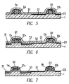
- the remaining part of the resist layer 20 is removed in such a way as to obtain the structure illustrated by the diagram in FIG. 4 .
- the regions not to be silicided are again exposed.
- This removal step may be carried out by any known method, especially by chemical etching. As illustrated, this removal leaves the compound portions 21 , 22 and 23 intact, since this compound is resistant to the chemical etching commonly used in microelectronics, especially etching by an oxidizing plasma or by HF.
- a metal layer 30 is deposited on the structure, the said metal being suitable for forming a silicide by thermal annealing.
- the layer 30 is a conformal layer that covers all the exposed parts of the structure, in particular the gate, source and drain regions of the two transistors 10 a and 10 b .
- the metal layer covers both the regions to be silicided and the regions not to be silicided.
- This deposition may be carried out by any conventional process, especially by a process of sputtering.
- Metals that have the property of reacting with silicon in order to form a silicide, thus forming good candidates since they have well-controlled deposition processes, are especially Co, nickel (Ni), platinum (Pt) and titanium (Ti). Their corresponding silicides are CoSi 2 , NiSi, PtSi and TiSi 2 , respectively.
- a heat treatment for example an RTP (Rapid Thermal Processing) heat treatment, i.e., a heating step.
- This heating step results in the formation of silicide layers 31 and 33 on the surface of the source and drain regions of the transistor 10 a and of a similar layer 32 on the surface of the gate region 11 a of this transistor.
- the presence of the implantation residue layers 21 , 22 and 23 on the corresponding regions of the transistor 10 b prevents the formation of a silicide on the surface of these regions.
- the implantation residue layers 21 , 22 and 23 create a barrier to the formation of silicide at the interface between the metal layer 30 and the subjacent silicon portions.
- the remainder of the metal layer 30 is removed in order to obtain the configuration shown in FIG. 7 .
- This removal may be carried out by any conventional method, especially by chemical etching.
- the implantation of the non-dopant ions through the resist layer 20 creates a screen which then prevents the siliciding of the regions that have been beneath the resist during the said implantation.
- the desired selected siliciding is obtained.
- implementation of the invention can be readily detected in semiconductor devices. This is because it may be seen that the TEOS and nitride layers are absent, these layers would have remained in the unsilicided regions when a process according to the prior art described in the introduction is employed. As a variant or as a complement, it is also possible to show the presence of implantation residues in the unsilicided regions. This may be achieved by compositional analysis using SIMS (Secondary Ion Mass Spectroscopy) or using a technique for detecting impurities in the silicon, of the Auger type or the like. This analysis and this technique are well known to those skilled in the art.
- SIMS Secondary Ion Mass Spectroscopy
- the invention also relates to a semiconductor device obtained by implementing a process as described above.
Landscapes
- Engineering & Computer Science (AREA)
- Physics & Mathematics (AREA)
- Condensed Matter Physics & Semiconductors (AREA)
- General Physics & Mathematics (AREA)
- Manufacturing & Machinery (AREA)
- Computer Hardware Design (AREA)
- Microelectronics & Electronic Packaging (AREA)
- Power Engineering (AREA)
- Electrodes Of Semiconductors (AREA)
- Insulated Gate Type Field-Effect Transistor (AREA)
Abstract
Description
Claims (20)
Applications Claiming Priority (2)
| Application Number | Priority Date | Filing Date | Title |
|---|---|---|---|
| FR0307474A FR2856514A1 (en) | 2003-06-20 | 2003-06-20 | PROCESS FOR THE SELECTIVE FORMATION OF SILICIDE ON A PLATE OF SEMICONDUCTOR MATERIAL |
| FR0307474 | 2003-06-20 |
Publications (2)
| Publication Number | Publication Date |
|---|---|
| US20050064638A1 US20050064638A1 (en) | 2005-03-24 |
| US7022595B2 true US7022595B2 (en) | 2006-04-04 |
Family
ID=33396821
Family Applications (1)
| Application Number | Title | Priority Date | Filing Date |
|---|---|---|---|
| US10/871,356 Active US7022595B2 (en) | 2003-06-20 | 2004-06-18 | Method for the selective formation of a silicide on a wafer using an implantation residue layer |
Country Status (3)
| Country | Link |
|---|---|
| US (1) | US7022595B2 (en) |
| EP (1) | EP1489648A1 (en) |
| FR (1) | FR2856514A1 (en) |
Cited By (1)
| Publication number | Priority date | Publication date | Assignee | Title |
|---|---|---|---|---|
| US20100013090A1 (en) * | 2006-09-29 | 2010-01-21 | Nxp, B.V. | Silicide formation on a wafer |
Families Citing this family (2)
| Publication number | Priority date | Publication date | Assignee | Title |
|---|---|---|---|---|
| US8987102B2 (en) * | 2011-07-27 | 2015-03-24 | Applied Materials, Inc. | Methods of forming a metal silicide region in an integrated circuit |
| US9972694B2 (en) * | 2015-10-20 | 2018-05-15 | Taiwan Semiconductor Manufacturing Company, Ltd. | Atomic layer deposition methods and structures thereof |
Citations (13)
| Publication number | Priority date | Publication date | Assignee | Title |
|---|---|---|---|---|
| US4729969A (en) | 1985-09-05 | 1988-03-08 | Mitsubishi Denki Kabushiki Kaisha | Method for forming silicide electrode in semiconductor device |
| US4861732A (en) * | 1987-10-15 | 1989-08-29 | Fujitsu Limited | Method for removing an ion-implanted organic resin layer during fabrication of semiconductor devices |
| US5258637A (en) | 1991-09-23 | 1993-11-02 | Micron Technology, Inc. | Semiconductor devices produced according to a method which reduces contact resistance at silicide/active area interfaces |
| US5705441A (en) | 1996-03-19 | 1998-01-06 | Taiwan Semiconductor Manufacturing Company, Ltd. | Ion implant silicon nitride mask for a silicide free contact region in a self aligned silicide process |
| US6001737A (en) | 1996-03-29 | 1999-12-14 | Nec Corporation | Method of forming a semiconductor device having a titanium salicide shallow junction diffusion layer |
| US6004871A (en) | 1996-06-03 | 1999-12-21 | Texas Instruments Incorporated | Implant enhancement of titanium silicidation |
| WO2000036634A2 (en) | 1998-12-16 | 2000-06-22 | Intel Corporation | Amorphization of substrate to prevent silicide encroachment into channel region of field effect transistor |
| US6255179B1 (en) | 1999-08-04 | 2001-07-03 | International Business Machines Corporation | Plasma etch pre-silicide clean |
| US6281556B1 (en) | 1998-03-13 | 2001-08-28 | Stmicroelectronics S.A. | Process for forming a low resistivity titanium silicide layer on a silicon semiconductor substrate and the resulting device |
| US6326289B1 (en) * | 1998-08-24 | 2001-12-04 | Texas Instruments Incorporated | Method of forming a silicide layer using a pre-amorphization implant which is blocked from source/drain regions by a layer of photoresist |
| US20020064918A1 (en) | 2000-11-29 | 2002-05-30 | Lee Pooi See | Method and apparatus for performing nickel salicidation |
| US20020098689A1 (en) | 2000-07-03 | 2002-07-25 | Chartered Semiconductor Manufacturing Ltd. | Formation of silicided shallow junctions using implant through metal technology and laser annealing process |
| US20020155690A1 (en) | 2001-04-18 | 2002-10-24 | International Business Machines Corporation | Self-aligned silicide process for silicon sidewall source and drain contacts and structure formed thereby |
-
2003
- 2003-06-20 FR FR0307474A patent/FR2856514A1/en active Pending
-
2004
- 2004-06-07 EP EP04291417A patent/EP1489648A1/en not_active Withdrawn
- 2004-06-18 US US10/871,356 patent/US7022595B2/en active Active
Patent Citations (13)
| Publication number | Priority date | Publication date | Assignee | Title |
|---|---|---|---|---|
| US4729969A (en) | 1985-09-05 | 1988-03-08 | Mitsubishi Denki Kabushiki Kaisha | Method for forming silicide electrode in semiconductor device |
| US4861732A (en) * | 1987-10-15 | 1989-08-29 | Fujitsu Limited | Method for removing an ion-implanted organic resin layer during fabrication of semiconductor devices |
| US5258637A (en) | 1991-09-23 | 1993-11-02 | Micron Technology, Inc. | Semiconductor devices produced according to a method which reduces contact resistance at silicide/active area interfaces |
| US5705441A (en) | 1996-03-19 | 1998-01-06 | Taiwan Semiconductor Manufacturing Company, Ltd. | Ion implant silicon nitride mask for a silicide free contact region in a self aligned silicide process |
| US6001737A (en) | 1996-03-29 | 1999-12-14 | Nec Corporation | Method of forming a semiconductor device having a titanium salicide shallow junction diffusion layer |
| US6004871A (en) | 1996-06-03 | 1999-12-21 | Texas Instruments Incorporated | Implant enhancement of titanium silicidation |
| US6281556B1 (en) | 1998-03-13 | 2001-08-28 | Stmicroelectronics S.A. | Process for forming a low resistivity titanium silicide layer on a silicon semiconductor substrate and the resulting device |
| US6326289B1 (en) * | 1998-08-24 | 2001-12-04 | Texas Instruments Incorporated | Method of forming a silicide layer using a pre-amorphization implant which is blocked from source/drain regions by a layer of photoresist |
| WO2000036634A2 (en) | 1998-12-16 | 2000-06-22 | Intel Corporation | Amorphization of substrate to prevent silicide encroachment into channel region of field effect transistor |
| US6255179B1 (en) | 1999-08-04 | 2001-07-03 | International Business Machines Corporation | Plasma etch pre-silicide clean |
| US20020098689A1 (en) | 2000-07-03 | 2002-07-25 | Chartered Semiconductor Manufacturing Ltd. | Formation of silicided shallow junctions using implant through metal technology and laser annealing process |
| US20020064918A1 (en) | 2000-11-29 | 2002-05-30 | Lee Pooi See | Method and apparatus for performing nickel salicidation |
| US20020155690A1 (en) | 2001-04-18 | 2002-10-24 | International Business Machines Corporation | Self-aligned silicide process for silicon sidewall source and drain contacts and structure formed thereby |
Cited By (2)
| Publication number | Priority date | Publication date | Assignee | Title |
|---|---|---|---|---|
| US20100013090A1 (en) * | 2006-09-29 | 2010-01-21 | Nxp, B.V. | Silicide formation on a wafer |
| US9379020B2 (en) | 2006-09-29 | 2016-06-28 | Nxp B.V. | Silicide formation on a wafer |
Also Published As
| Publication number | Publication date |
|---|---|
| EP1489648A1 (en) | 2004-12-22 |
| US20050064638A1 (en) | 2005-03-24 |
| FR2856514A1 (en) | 2004-12-24 |
Similar Documents
| Publication | Publication Date | Title |
|---|---|---|
| CN101661904B (en) | Semiconductor device and method for fabricating same | |
| US7148097B2 (en) | Integrated circuit containing polysilicon gate transistors and fully silicidized metal gate transistors | |
| US6930007B2 (en) | Integration of pre-S/D anneal selective nitride/oxide composite cap for improving transistor performance | |
| US7078285B1 (en) | SiGe nickel barrier structure employed in a CMOS device to prevent excess diffusion of nickel used in the silicide material | |
| US7737015B2 (en) | Formation of fully silicided gate with oxide barrier on the source/drain silicide regions | |
| US8643126B2 (en) | Self aligned silicided contacts | |
| US7253049B2 (en) | Method for fabricating dual work function metal gates | |
| KR20050116433A (en) | Method of manufacturing semiconductor device | |
| US20080237867A1 (en) | Low contact resistance metal contact | |
| US6555438B1 (en) | Method for fabricating MOSFETs with a recessed self-aligned silicide contact and extended source/drain junctions | |
| US7397073B2 (en) | Barrier dielectric stack for seam protection | |
| US7745292B2 (en) | Method for fabricating a semiconductor gate structure | |
| US20070099407A1 (en) | Method for fabricating a transistor using a low temperature spike anneal | |
| JPH08213610A (en) | Field effect transistor and its manufacturing method | |
| US20050253204A1 (en) | Method of forming silicided gate structure | |
| US7022595B2 (en) | Method for the selective formation of a silicide on a wafer using an implantation residue layer | |
| US20080122016A1 (en) | Semiconductor device and fabricating method thereof | |
| US7687396B2 (en) | Method of forming silicided gates using buried metal layers | |
| KR20090076937A (en) | Silicide formation on a wafer | |
| US20080299767A1 (en) | Method for Forming a Semiconductor Device Having a Salicide Layer | |
| US20050064691A1 (en) | Semiconductor devices and methods for fabricating a silicide of a semiconductor device | |
| KR100600380B1 (en) | Making Method of Semiconductor Device | |
| US20110097867A1 (en) | Method of controlling gate thicknesses in forming fusi gates | |
| US6777300B2 (en) | Method to improve silicide formation on polysilicon | |
| US7851874B2 (en) | Semiconductor device and method for manufacturing the same |
Legal Events
| Date | Code | Title | Description |
|---|---|---|---|
| AS | Assignment |
Owner name: STMICROELECTRONICS SA, FRANCE Free format text: ASSIGNMENT OF ASSIGNORS INTEREST;ASSIGNORS:REGNIER, CHRISTOPHE;WACQUANT, FRANCOIS;REEL/FRAME:015392/0601 Effective date: 20041020 |
|
| FEPP | Fee payment procedure |
Free format text: PAYOR NUMBER ASSIGNED (ORIGINAL EVENT CODE: ASPN); ENTITY STATUS OF PATENT OWNER: LARGE ENTITY |
|
| STCF | Information on status: patent grant |
Free format text: PATENTED CASE |
|
| CC | Certificate of correction | ||
| FEPP | Fee payment procedure |
Free format text: PAYOR NUMBER ASSIGNED (ORIGINAL EVENT CODE: ASPN); ENTITY STATUS OF PATENT OWNER: LARGE ENTITY Free format text: PAYER NUMBER DE-ASSIGNED (ORIGINAL EVENT CODE: RMPN); ENTITY STATUS OF PATENT OWNER: LARGE ENTITY |
|
| FPAY | Fee payment |
Year of fee payment: 4 |
|
| FPAY | Fee payment |
Year of fee payment: 8 |
|
| MAFP | Maintenance fee payment |
Free format text: PAYMENT OF MAINTENANCE FEE, 12TH YEAR, LARGE ENTITY (ORIGINAL EVENT CODE: M1553) Year of fee payment: 12 |
|
| AS | Assignment |
Owner name: STMICROELECTRONICS FRANCE, FRANCE Free format text: CHANGE OF NAME;ASSIGNOR:STMICROELECTRONICS SA;REEL/FRAME:066850/0496 Effective date: 20230126 |