US7019511B1 - Optical analysis of integrated circuits - Google Patents
Optical analysis of integrated circuits Download PDFInfo
- Publication number
- US7019511B1 US7019511B1 US09/755,008 US75500801A US7019511B1 US 7019511 B1 US7019511 B1 US 7019511B1 US 75500801 A US75500801 A US 75500801A US 7019511 B1 US7019511 B1 US 7019511B1
- Authority
- US
- United States
- Prior art keywords
- soi
- integrated circuit
- silicon
- die
- arrangement
- Prior art date
- Legal status (The legal status is an assumption and is not a legal conclusion. Google has not performed a legal analysis and makes no representation as to the accuracy of the status listed.)
- Expired - Fee Related, expires
Links
- 230000003287 optical effect Effects 0.000 title claims abstract description 29
- 238000004458 analytical method Methods 0.000 title claims abstract description 21
- 229910052710 silicon Inorganic materials 0.000 claims abstract description 22
- 239000010703 silicon Substances 0.000 claims abstract description 22
- 238000000034 method Methods 0.000 claims abstract description 15
- 230000004044 response Effects 0.000 claims abstract description 15
- 239000012212 insulator Substances 0.000 claims abstract description 13
- 238000001514 detection method Methods 0.000 claims description 6
- 230000000007 visual effect Effects 0.000 claims description 6
- 230000008569 process Effects 0.000 claims description 4
- 238000012360 testing method Methods 0.000 claims description 4
- 230000005764 inhibitory process Effects 0.000 abstract 1
- XUIMIQQOPSSXEZ-UHFFFAOYSA-N Silicon Chemical compound [Si] XUIMIQQOPSSXEZ-UHFFFAOYSA-N 0.000 description 12
- 239000004065 semiconductor Substances 0.000 description 11
- 239000000758 substrate Substances 0.000 description 6
- 230000002950 deficient Effects 0.000 description 5
- 238000004519 manufacturing process Methods 0.000 description 5
- VYPSYNLAJGMNEJ-UHFFFAOYSA-N Silicium dioxide Chemical compound O=[Si]=O VYPSYNLAJGMNEJ-UHFFFAOYSA-N 0.000 description 4
- 230000007547 defect Effects 0.000 description 4
- 230000006378 damage Effects 0.000 description 2
- 238000005530 etching Methods 0.000 description 2
- 238000012986 modification Methods 0.000 description 2
- 230000004048 modification Effects 0.000 description 2
- 229910021421 monocrystalline silicon Inorganic materials 0.000 description 2
- 238000004806 packaging method and process Methods 0.000 description 2
- 235000012239 silicon dioxide Nutrition 0.000 description 2
- 239000000377 silicon dioxide Substances 0.000 description 2
- 229910000679 solder Inorganic materials 0.000 description 2
- 230000000638 stimulation Effects 0.000 description 2
- VXEGSRKPIUDPQT-UHFFFAOYSA-N 4-[4-(4-methoxyphenyl)piperazin-1-yl]aniline Chemical compound C1=CC(OC)=CC=C1N1CCN(C=2C=CC(N)=CC=2)CC1 VXEGSRKPIUDPQT-UHFFFAOYSA-N 0.000 description 1
- KZBUYRJDOAKODT-UHFFFAOYSA-N Chlorine Chemical compound ClCl KZBUYRJDOAKODT-UHFFFAOYSA-N 0.000 description 1
- ZAMOUSCENKQFHK-UHFFFAOYSA-N Chlorine atom Chemical compound [Cl] ZAMOUSCENKQFHK-UHFFFAOYSA-N 0.000 description 1
- RTAQQCXQSZGOHL-UHFFFAOYSA-N Titanium Chemical compound [Ti] RTAQQCXQSZGOHL-UHFFFAOYSA-N 0.000 description 1
- 230000002411 adverse Effects 0.000 description 1
- 239000006227 byproduct Substances 0.000 description 1
- 229910052801 chlorine Inorganic materials 0.000 description 1
- 239000000460 chlorine Substances 0.000 description 1
- 239000004020 conductor Substances 0.000 description 1
- 229910021419 crystalline silicon Inorganic materials 0.000 description 1
- 230000007423 decrease Effects 0.000 description 1
- 230000003247 decreasing effect Effects 0.000 description 1
- 238000013461 design Methods 0.000 description 1
- 230000001066 destructive effect Effects 0.000 description 1
- 230000009977 dual effect Effects 0.000 description 1
- 238000005516 engineering process Methods 0.000 description 1
- MUJOIMFVNIBMKC-UHFFFAOYSA-N fludioxonil Chemical compound C=12OC(F)(F)OC2=CC=CC=1C1=CNC=C1C#N MUJOIMFVNIBMKC-UHFFFAOYSA-N 0.000 description 1
- 238000002844 melting Methods 0.000 description 1
- 230000008018 melting Effects 0.000 description 1
- 229910052751 metal Inorganic materials 0.000 description 1
- 239000002184 metal Substances 0.000 description 1
- 230000035515 penetration Effects 0.000 description 1
- 238000005498 polishing Methods 0.000 description 1
- 238000000275 quality assurance Methods 0.000 description 1
- 239000005049 silicon tetrachloride Substances 0.000 description 1
- 239000010936 titanium Substances 0.000 description 1
- 229910052719 titanium Inorganic materials 0.000 description 1
- 238000013024 troubleshooting Methods 0.000 description 1
Images


Classifications
-
- G—PHYSICS
- G01—MEASURING; TESTING
- G01R—MEASURING ELECTRIC VARIABLES; MEASURING MAGNETIC VARIABLES
- G01R31/00—Arrangements for testing electric properties; Arrangements for locating electric faults; Arrangements for electrical testing characterised by what is being tested not provided for elsewhere
- G01R31/28—Testing of electronic circuits, e.g. by signal tracer
- G01R31/302—Contactless testing
- G01R31/308—Contactless testing using non-ionising electromagnetic radiation, e.g. optical radiation
- G01R31/311—Contactless testing using non-ionising electromagnetic radiation, e.g. optical radiation of integrated circuits
-
- G—PHYSICS
- G01—MEASURING; TESTING
- G01N—INVESTIGATING OR ANALYSING MATERIALS BY DETERMINING THEIR CHEMICAL OR PHYSICAL PROPERTIES
- G01N21/00—Investigating or analysing materials by the use of optical means, i.e. using sub-millimetre waves, infrared, visible or ultraviolet light
- G01N21/17—Systems in which incident light is modified in accordance with the properties of the material investigated
- G01N21/1717—Systems in which incident light is modified in accordance with the properties of the material investigated with a modulation of one or more physical properties of the sample during the optical investigation, e.g. electro-reflectance
-
- G—PHYSICS
- G01—MEASURING; TESTING
- G01N—INVESTIGATING OR ANALYSING MATERIALS BY DETERMINING THEIR CHEMICAL OR PHYSICAL PROPERTIES
- G01N21/00—Investigating or analysing materials by the use of optical means, i.e. using sub-millimetre waves, infrared, visible or ultraviolet light
- G01N21/84—Systems specially adapted for particular applications
- G01N21/88—Investigating the presence of flaws or contamination
- G01N21/95—Investigating the presence of flaws or contamination characterised by the material or shape of the object to be examined
- G01N21/9501—Semiconductor wafers
-
- G—PHYSICS
- G01—MEASURING; TESTING
- G01N—INVESTIGATING OR ANALYSING MATERIALS BY DETERMINING THEIR CHEMICAL OR PHYSICAL PROPERTIES
- G01N21/00—Investigating or analysing materials by the use of optical means, i.e. using sub-millimetre waves, infrared, visible or ultraviolet light
- G01N21/17—Systems in which incident light is modified in accordance with the properties of the material investigated
- G01N21/1717—Systems in which incident light is modified in accordance with the properties of the material investigated with a modulation of one or more physical properties of the sample during the optical investigation, e.g. electro-reflectance
- G01N2021/1721—Electromodulation
-
- G—PHYSICS
- G01—MEASURING; TESTING
- G01R—MEASURING ELECTRIC VARIABLES; MEASURING MAGNETIC VARIABLES
- G01R31/00—Arrangements for testing electric properties; Arrangements for locating electric faults; Arrangements for electrical testing characterised by what is being tested not provided for elsewhere
- G01R31/28—Testing of electronic circuits, e.g. by signal tracer
- G01R31/302—Contactless testing
- G01R31/304—Contactless testing of printed or hybrid circuits
Definitions
- the present invention relates generally to semiconductor devices and their fabrication and, more particularly, to semiconductor devices and their manufacture involving techniques for analyzing and debugging circuitry within an integrated circuit.
- DIP dual in-line package
- flip chip packaging uses the bonding pads and metal (solder) bumps.
- the bonding pads need not be on the periphery of the die and hence are moved to the site nearest the transistors and other circuit devices formed in the die. As a result, the electrical path to the pad is shorter. Electrical connections to the package are made when the die is flipped over the package with corresponding bonding pads. Each bump connects to a corresponding package inner lead. The resulting packages have a lower profile and have lower electrical resistance and a shortened electrical path.
- the output terminals of the package may be ball-shaped conductive-bump contacts (usually solder or other similar conductive material) and are typically disposed in a rectangular array. These packages are occasionally referred to as “Ball Grid Array” (BGA). Alternatively, the output terminals of the package may be pins, and such a package is commonly known as the pin grid array (PGA) package.
- BGA Ball Grid Array
- PGA pin grid array
- the transistors and other circuitry are generally formed in a very thin epitaxially grown silicon layer on a single crystal silicon wafer of which the die is singulated from.
- a layer of insulating silicon dioxide is formed on one surface of a single crystal silicon wafer followed by the thin epitaxially grown silicon layer containing the transistors and other circuitry.
- This wafer structure is termed “silicon on insulator” (SOI) and the silicon dioxide layer is called the buried oxide layer (BOX).
- SOI silicon on insulator
- BOX buried oxide layer
- the epitaxial silicon layer is typically about 10 micrometers thick, the buried oxide layer less than about 1 micrometer, and the bulk silicon greater than 500 micrometers.
- the transistors formed on the SOI structure show decreased drain capacitance, resulting in a faster switch transistor.
- the side of the die including the epitaxial layer containing the transistors and the other active circuitry is often referred to as the circuit side of the die or front side of the die.
- the circuit side of the die is positioned very near the package.
- the circuit side opposes the backside of the die.
- Between the backside and the circuit side of the die is single crystalline silicon and, in the case of SOI circuits, also a buried oxide layer. The positioning of the circuit side provides many of the advantages of the flip chip.
- the present invention is directed to a method and system for optical beam analysis of a semiconductor device having SOI structure.
- the present invention is exemplified in a number of implementations and applications, some of which are summarized below.
- a modulated optical beam is directed at a selected portion of an integrated circuit having silicon on insulator (SOI) structure.
- SOI silicon on insulator
- the modulation of the beam is selected to sufficiently inhibit intrusion of the beam upon the integrated circuit.
- a reflected optical waveform response is obtained therefrom for use in analyzing the device. In this manner, analysis of an integrated circuit having SOI structure is achieved without necessarily destroying or modifying the integrated circuit structure.
- a SOI integrated circuit die having a circuit side opposite a back side is placed in an analysis arrangement.
- An infrared laser is arranged to direct a laser beam into the back side and to a selected portion in the die.
- the laser is pulsed at intervals having a duration of about 100 femto-seconds, the interval being selected to sufficiently inhibit intrusion of the laser upon the die.
- the die is operated and a waveform is obtained as a function of the operation of the die and a reflection of the optical beam. The waveform is then used for die analysis, such as troubleshooting, defect detection, quality assurance or design testing.
- FIG. 1 illustrates a SOI flip chip undergoing analysis, according to an example embodiment of the present invention
- FIG. 2 illustrates a SOI flip chip undergoing analysis, according to another example embodiment of the present invention.
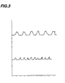
- FIG. 3 is a graphic representation of waveforms acquired from a SOI flip chip die, according to another example embodiment of the present invention.
- the present invention is believed to be applicable for a variety of different types of semiconductor devices, and the invention has been found to be particularly suited for analyzing silicon on insulator (SOI) integrated circuit dies. While the present invention is not necessarily limited to such SOI devices, various aspects of the invention may be appreciated through a discussion of various examples using this context.
- SOI silicon on insulator
- an optical beam is directed at a selected portion of a conventional flip chip type SOI die.
- the beam is pulsed at an interval that is sufficient to inhibit intrusion of the beam into the die.
- a reflected optical response from the SOI is obtained from the die and used to generate a waveform representing an electrical characteristic of the die.
- enough substrate is removed from a back side of an SOI die to facilitate penetration of an infrared laser beam to a selected portion within the die.
- an infrared laser beam is directed at the back side of the die.
- the beam is focused at a circuitry node of interest located at a specific depth within a circuitry layer of the die.
- the beam is pulsed at a duration in the femto-second-range (e.g., about 100 femto-seconds long), and the pulsed beam passes through the back side to the node.
- a reflected beam response is obtained from the node of interest, and characteristics of the reflection are used to generate a voltage waveform that is used to analyze the die.
- the femto-second pulse duration aids in analysis of circuitry operating at high frequency, and in circuitry located such that analysis using a laser having a longer pulse or constant application would harm the die.
- analysis may include comparing the waveform response obtained from the die with responses from defective or non-defective integrated circuit dies of similar structure and configuration.
- FIG. 1 shows a SOI die 15 with a modulated laser beam 120 directed at a circuitry node 122 of interest located at a specific depth in the circuitry layer.
- the beam passes through a back side 30 of the die to the node 122 and reflects as beam 130 that can be used to analyze the die circuitry.
- the laser beam 120 is modulated in a manner that makes possible the detection of a response from the node 122 without adversely affecting surrounding circuitry and interconnects.
- the laser modulation is particularly useful for analyzing dies having circuitry located in close proximity and for accessing circuitry located below another circuit layer, as shown in FIG. 1 .
- the die can be prepared in various manners for analysis. According to an example embodiment of the present invention, the die is thinned prior to analysis. In one implementation, the back side is globally thinned and the beam 120 is directed through the globally thinned surface, such as shown by dashed lines in FIG. 1 . Mechanical polishing is one method for global thinning. In another implementation, the die 15 receives two or three steps of thinning in the process. After the die is globally thinned, local thinning techniques, such as laser microchemical etching, are then used to thin the silicon in an area to a level that is thinner than the die size as shown by exposed region 32 .
- local thinning techniques such as laser microchemical etching
- One method for laser microchemical etching of silicon is focusing a laser beam on the backside of the silicon surface to cause local melting of silicon in the presence of chlorine gas.
- the molten silicon reacts very rapidly with chlorine and forms silicon tetrachloride gas, which leaves the molten (reaction) zone.
- the thinned die 15 is analyzed as described herein.
- FIG. 2 shows a side view of a SOI die 15 having a circuit side 20 and a backside 30 undergoing analysis according to an example embodiment of the invention.
- a system 100 is adapted to obtain non-contact optical waveform responses from devices and structures in the die 15 .
- An optical beam arrangement 110 such as a laser, generates a modulated beam 120 and is arranged to direct the beam at the backside 30 of the SOI die 15 .
- the beam 120 passes through a portion of the SOI die and reflects from a node in an epitaxial layer 22 , resulting in reflected beam 130 .
- Arrangement 140 detects the reflected beam 130 in a manner that makes possible analysis of the die 15 therefrom.
- the beam arrangement 110 is adapted to generate an infrared laser beam that is pulsed at a duration in the femto-second (10 ⁇ 15 ) range.
- a femto-second laser suitable for use in connection with the present invention is the titanium:saphire laser commercially available from a number of sources, including CDP Laser and Scanning Systems of Moscow, Russia.
- the beam is focused on the node at a selected depth in the exptaxial layer 22 .
- the focused nature of the laser beam 120 allows the system 100 to pinpoint a specific circuitry node in the epitaxial layer structure 22 .
- the short laser pulse duration imposes a minimal intrusion on the area of interest of the SOI flip chip 15 , and the infrared beam 120 limits the energy impinging on the die 15 .
- the depth focusing ability, coupled with the minimal intrusion upon the die 15 is useful in dies of complex circuitry containing multiple stacked layers of components.
- the system 100 is further adapted to stimulate the die circuitry, and obtains optical waveforms from the reflected laser beam 130 that are responsive to the stimulus.
- the stimulation may include, for example, applying a test vector pattern including a series of voltage inputs to the circuit that cause the die to operate under normal or failure conditions.
- the stimulation can be applied in a loop that cycles the circuit through one or more failure conditions. The system 100 then obtains a response from the circuit receiving the stimulus.
- a computer arrangement 150 is coupled to the detection arrangement 140 .
- the computer arrangement 150 is adapted to receive and process the reflected optical waveform response 130 collected by the detection arrangement 140 .
- a visual output arrangement 160 may be coupled to the computer arrangement 150 and adapted to present data from the computer arrangement 150 for visual analysis.
- the visual output arrangement 160 may include a video monitor and a printer.
- the computer arrangement 150 may also include waveform analysis software for further analysis of the reflected modulated optical waveform response 130 collected by the detection arrangement 140 .
- Example responses include voltage waveforms acquired from the system detector 140 , such as shown in FIG. 3 .
- Voltage waveforms such as that shown in FIG. 3 can be used to detect a defect or verify performance of an integrate circuit die in various manners. For instance, the voltage waveform can be compared to a reference waveform from a die known to exhibit a defect for which the die being analyzed is suspected to have. The waveform can also be compared to that of a die that is known to be non-defective. Variations in the waveform can then be used to detect a defect.
Landscapes
- Physics & Mathematics (AREA)
- Health & Medical Sciences (AREA)
- Engineering & Computer Science (AREA)
- General Physics & Mathematics (AREA)
- Analytical Chemistry (AREA)
- General Health & Medical Sciences (AREA)
- Pathology (AREA)
- Immunology (AREA)
- Biochemistry (AREA)
- Chemical & Material Sciences (AREA)
- Life Sciences & Earth Sciences (AREA)
- Microelectronics & Electronic Packaging (AREA)
- Computer Hardware Design (AREA)
- General Engineering & Computer Science (AREA)
- Computer Vision & Pattern Recognition (AREA)
- Toxicology (AREA)
- Electromagnetism (AREA)
- Testing Or Measuring Of Semiconductors Or The Like (AREA)
- Tests Of Electronic Circuits (AREA)
Abstract
Description
Claims (9)
Priority Applications (1)
| Application Number | Priority Date | Filing Date | Title |
|---|---|---|---|
| US09/755,008 US7019511B1 (en) | 2001-01-05 | 2001-01-05 | Optical analysis of integrated circuits |
Applications Claiming Priority (1)
| Application Number | Priority Date | Filing Date | Title |
|---|---|---|---|
| US09/755,008 US7019511B1 (en) | 2001-01-05 | 2001-01-05 | Optical analysis of integrated circuits |
Publications (1)
| Publication Number | Publication Date |
|---|---|
| US7019511B1 true US7019511B1 (en) | 2006-03-28 |
Family
ID=36084623
Family Applications (1)
| Application Number | Title | Priority Date | Filing Date |
|---|---|---|---|
| US09/755,008 Expired - Fee Related US7019511B1 (en) | 2001-01-05 | 2001-01-05 | Optical analysis of integrated circuits |
Country Status (1)
| Country | Link |
|---|---|
| US (1) | US7019511B1 (en) |
Cited By (2)
| Publication number | Priority date | Publication date | Assignee | Title |
|---|---|---|---|---|
| US20070229096A1 (en) * | 2006-03-31 | 2007-10-04 | Chu Tan V | System and method for detecting single event latchup in integrated circuits |
| US20090096113A1 (en) * | 2007-10-16 | 2009-04-16 | Honeywell International Inc. | SOI on Package Hypersensitive Sensor |
Citations (3)
| Publication number | Priority date | Publication date | Assignee | Title |
|---|---|---|---|---|
| US5381421A (en) * | 1990-01-12 | 1995-01-10 | International Business Machines Corporation | Per pin circuit test system having N-bit pin interface providing speed improvement with frequency multiplexing |
| US5999006A (en) * | 1996-09-30 | 1999-12-07 | Nec Corporation | Method of and apparatus for conducting analysis of buried oxides |
| US6072179A (en) * | 1998-08-07 | 2000-06-06 | Intel Corporation | Method and apparatus using an infrared laser based optical probe for measuring voltages directly from active regions in an integrated circuit |
-
2001
- 2001-01-05 US US09/755,008 patent/US7019511B1/en not_active Expired - Fee Related
Patent Citations (3)
| Publication number | Priority date | Publication date | Assignee | Title |
|---|---|---|---|---|
| US5381421A (en) * | 1990-01-12 | 1995-01-10 | International Business Machines Corporation | Per pin circuit test system having N-bit pin interface providing speed improvement with frequency multiplexing |
| US5999006A (en) * | 1996-09-30 | 1999-12-07 | Nec Corporation | Method of and apparatus for conducting analysis of buried oxides |
| US6072179A (en) * | 1998-08-07 | 2000-06-06 | Intel Corporation | Method and apparatus using an infrared laser based optical probe for measuring voltages directly from active regions in an integrated circuit |
Cited By (4)
| Publication number | Priority date | Publication date | Assignee | Title |
|---|---|---|---|---|
| US20070229096A1 (en) * | 2006-03-31 | 2007-10-04 | Chu Tan V | System and method for detecting single event latchup in integrated circuits |
| US7830165B2 (en) * | 2006-03-31 | 2010-11-09 | Integrated Device Technology, Inc. | System and method for detecting single event latchup in integrated circuits |
| US20090096113A1 (en) * | 2007-10-16 | 2009-04-16 | Honeywell International Inc. | SOI on Package Hypersensitive Sensor |
| US7868362B2 (en) | 2007-10-16 | 2011-01-11 | Honeywell International Inc. | SOI on package hypersensitive sensor |
Similar Documents
| Publication | Publication Date | Title |
|---|---|---|
| US5838159A (en) | Chip carrier to allow electron beam probing and FIB modifications | |
| EP0577333B1 (en) | Temporary connections for fast electrical access to electronic devices | |
| US5719449A (en) | Flip-chip integrated circuit with improved testability | |
| US6285036B1 (en) | Endpoint detection for thinning of silicon of a flip chip bonded integrated circuit | |
| US6020746A (en) | Method and apparatus for probing an integrated circuit through the back side of an integrated circuit die | |
| US6480012B1 (en) | Probe card device | |
| US6210981B1 (en) | Method for etching a flip chip using secondary particle emissions to detect the etch end-point | |
| US6403388B1 (en) | Nanomachining method for integrated circuits | |
| US7279343B1 (en) | De-packaging process for small outline transistor packages | |
| US6894522B2 (en) | Specific site backside underlaying and micromasking method for electrical characterization of semiconductor devices | |
| US6255124B1 (en) | Test arrangement and method for thinned flip chip IC | |
| US6417680B1 (en) | Method and apparatus for stress testing a semiconductor device using laser-induced circuit excitation | |
| US7019511B1 (en) | Optical analysis of integrated circuits | |
| US6500699B1 (en) | Test fixture for future integration | |
| JPH11154695A (en) | Method for locating faulty point on integrated circuit and apparatus for locating faulty point | |
| US6372627B1 (en) | Method and arrangement for characterization of focused-ion-beam insulator deposition | |
| US6281029B1 (en) | Probe points for heat dissipation during testing of flip chip IC | |
| US6277659B1 (en) | Substrate removal using thermal analysis | |
| US6177989B1 (en) | Laser induced current for semiconductor defect detection | |
| US6252239B1 (en) | Substrate removal from a semiconductor chip structure having buried insulator (BIN) | |
| US6541987B1 (en) | Laser-excited detection of defective semiconductor device | |
| US6545490B1 (en) | Trench-filled probe point for a semiconductor device | |
| US6428718B1 (en) | Selective back side wet etch | |
| US6518783B1 (en) | Circuit construction in back side of die and over a buried insulator | |
| US6621281B1 (en) | SOI die analysis of circuitry logic states via coupling through the insulator |
Legal Events
| Date | Code | Title | Description |
|---|---|---|---|
| AS | Assignment |
Owner name: ADVANCED MIRCRO DEVICES, INC., TEXAS Free format text: ASSIGNMENT OF ASSIGNORS INTEREST;ASSIGNORS:BIRDSLEY, JEFFREY D.;BRUCE, MICHAEL R.;DAVIS, BRENNAN V.;AND OTHERS;REEL/FRAME:011764/0970;SIGNING DATES FROM 20001110 TO 20001220 |
|
| FEPP | Fee payment procedure |
Free format text: PAYOR NUMBER ASSIGNED (ORIGINAL EVENT CODE: ASPN); ENTITY STATUS OF PATENT OWNER: LARGE ENTITY |
|
| AS | Assignment |
Owner name: GLOBALFOUNDRIES INC., CAYMAN ISLANDS Free format text: AFFIRMATION OF PATENT ASSIGNMENT;ASSIGNOR:ADVANCED MICRO DEVICES, INC.;REEL/FRAME:023119/0083 Effective date: 20090630 |
|
| FPAY | Fee payment |
Year of fee payment: 4 |
|
| FPAY | Fee payment |
Year of fee payment: 8 |
|
| FEPP | Fee payment procedure |
Free format text: MAINTENANCE FEE REMINDER MAILED (ORIGINAL EVENT CODE: REM.) |
|
| LAPS | Lapse for failure to pay maintenance fees |
Free format text: PATENT EXPIRED FOR FAILURE TO PAY MAINTENANCE FEES (ORIGINAL EVENT CODE: EXP.) |
|
| STCH | Information on status: patent discontinuation |
Free format text: PATENT EXPIRED DUE TO NONPAYMENT OF MAINTENANCE FEES UNDER 37 CFR 1.362 |
|
| FP | Lapsed due to failure to pay maintenance fee |
Effective date: 20180328 |
|
| AS | Assignment |
Owner name: GLOBALFOUNDRIES U.S. INC., NEW YORK Free format text: RELEASE BY SECURED PARTY;ASSIGNOR:WILMINGTON TRUST, NATIONAL ASSOCIATION;REEL/FRAME:056987/0001 Effective date: 20201117 |