US7012378B1 - Programmable current source and methods of use - Google Patents
Programmable current source and methods of use Download PDFInfo
- Publication number
- US7012378B1 US7012378B1 US10/773,962 US77396204A US7012378B1 US 7012378 B1 US7012378 B1 US 7012378B1 US 77396204 A US77396204 A US 77396204A US 7012378 B1 US7012378 B1 US 7012378B1
- Authority
- US
- United States
- Prior art keywords
- current source
- current
- output
- source circuits
- storage circuitry
- Prior art date
- Legal status (The legal status is an assumption and is not a legal conclusion. Google has not performed a legal analysis and makes no representation as to the accuracy of the status listed.)
- Expired - Fee Related, expires
Links
Images


Classifications
-
- G—PHYSICS
- G09—EDUCATION; CRYPTOGRAPHY; DISPLAY; ADVERTISING; SEALS
- G09G—ARRANGEMENTS OR CIRCUITS FOR CONTROL OF INDICATING DEVICES USING STATIC MEANS TO PRESENT VARIABLE INFORMATION
- G09G3/00—Control arrangements or circuits, of interest only in connection with visual indicators other than cathode-ray tubes
- G09G3/20—Control arrangements or circuits, of interest only in connection with visual indicators other than cathode-ray tubes for presentation of an assembly of a number of characters, e.g. a page, by composing the assembly by combination of individual elements arranged in a matrix no fixed position being assigned to or needed to be assigned to the individual characters or partial characters
- G09G3/22—Control arrangements or circuits, of interest only in connection with visual indicators other than cathode-ray tubes for presentation of an assembly of a number of characters, e.g. a page, by composing the assembly by combination of individual elements arranged in a matrix no fixed position being assigned to or needed to be assigned to the individual characters or partial characters using controlled light sources
- G09G3/30—Control arrangements or circuits, of interest only in connection with visual indicators other than cathode-ray tubes for presentation of an assembly of a number of characters, e.g. a page, by composing the assembly by combination of individual elements arranged in a matrix no fixed position being assigned to or needed to be assigned to the individual characters or partial characters using controlled light sources using electroluminescent panels
- G09G3/32—Control arrangements or circuits, of interest only in connection with visual indicators other than cathode-ray tubes for presentation of an assembly of a number of characters, e.g. a page, by composing the assembly by combination of individual elements arranged in a matrix no fixed position being assigned to or needed to be assigned to the individual characters or partial characters using controlled light sources using electroluminescent panels semiconductive, e.g. using light-emitting diodes [LED]
-
- G—PHYSICS
- G09—EDUCATION; CRYPTOGRAPHY; DISPLAY; ADVERTISING; SEALS
- G09G—ARRANGEMENTS OR CIRCUITS FOR CONTROL OF INDICATING DEVICES USING STATIC MEANS TO PRESENT VARIABLE INFORMATION
- G09G2300/00—Aspects of the constitution of display devices
- G09G2300/08—Active matrix structure, i.e. with use of active elements, inclusive of non-linear two terminal elements, in the pixels together with light emitting or modulating elements
- G09G2300/0809—Several active elements per pixel in active matrix panels
-
- G—PHYSICS
- G09—EDUCATION; CRYPTOGRAPHY; DISPLAY; ADVERTISING; SEALS
- G09G—ARRANGEMENTS OR CIRCUITS FOR CONTROL OF INDICATING DEVICES USING STATIC MEANS TO PRESENT VARIABLE INFORMATION
- G09G2310/00—Command of the display device
- G09G2310/02—Addressing, scanning or driving the display screen or processing steps related thereto
- G09G2310/0264—Details of driving circuits
- G09G2310/0272—Details of drivers for data electrodes, the drivers communicating data to the pixels by means of a current
Definitions
- Yet another object of the invention is to provide a new and improved programmable current source and a variety of calibration techniques that provides matched currents at multiple outputs.
- Still another object of the present invention is to provide a new and improved programmable current source that can be easily incorporated with virtually any circuitry requiring multiple constant current outputs.
- Each associated current source circuit of the plurality of current source circuits includes a master digital-to-analog converter coupled to the current level data storage circuitry of the associated current source circuit, a driver circuit having an input coupled to the master digital-to-analog converter and an output coupled to the output terminal of the associated current source circuit, comparator and storage circuitry having a first input coupled to the peak signal output terminal of the peak detector and storage circuitry, a second input coupled to the output of the driver circuit, and an output, and current level adjustment circuitry coupled to the output of the comparator and storage circuitry and the input of the driver circuit.
- the desired objects of the instant invention are further realized in accordance with a preferred method of calibrating a programmable multiple current source.
- the method includes a step of providing a plurality of current source circuits each including current level data storage circuitry, each of the plurality of current source circuits including an output terminal, and each of the plurality of current source circuits being constructed to operate at a plurality of current levels from a maximum current level to a minimum current level.
- the method also includes a step of supplying current level data representative of one current level in the plurality of current levels to the current level data storage circuitry in each of the plurality of current source circuits.
- Further steps in the method include receiving a plurality of output signals, one each representative of output current at each output terminal of the plurality of current source circuits and sensing a peak output signal in the plurality of received output signals, comparing the output signal representative of output current at each output terminal of the plurality of current source circuits to the sensed peak output signal to determine a difference and generating a plurality of adjustment signals, one each representative of the difference for each of the plurality of current source circuits, storing the plurality of adjustment signals, one each for each of the plurality of current source circuits, and using the stored plurality of adjustment signals, one each for each of the plurality of current source circuits, to adjust the output current at each output terminal of the plurality of current source circuits so that all of the plurality of current source circuits provide substantially matching output currents.
- FIG. 1 illustrates a programmable current source chip coupled to a system using multiple, programmable current source inputs
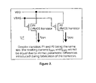
- FIGS. 2 and 3 illustrate typical constant current source circuits that exhibit a current skew problem
- FIG. 4 illustrates a typical example of the problem of providing matched currents at multiple outputs
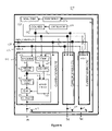
- FIG. 6 is a schematic of a programmable current source chip in accordance with the present invention.
- FIG. 7 is a schematic of a specific embodiment of a programmable current source chip in accordance with the present invention.
- FIG. 1 illustrates, generally, an electronic system 10 that includes a programmable current source integrated circuit chip 12 and an electronic circuit 14 connected to receive a plurality of currents N on a similar plurality of output leads 0 through N.
- Circuit 14 can be any circuit or application, such as a light emissive display, that requires multiple programmable current source inputs.
- Current source 12 accepts data and control signals on buses 16 and 18 , respectively, and delivers programmed constant electric currents on output leads 0 through N to circuit 14 .
- the problem that arises is that prior art constant current sources exhibit skew or mismatch due to intrinsic device parameters.
- TFT 1 0 and TFT 2 0 and the LED to a current return terminal.
- the intrinsic mismatch between the series connected devices in each pixel e.g. the difference between the series circuit TFT 1 0 , TFT 2 0 and the LED and the series circuit TFT 1 N , TFT 2 N and the LED
- the currents in this specific example I PIXEL(0) and I PIXEL(N) ).
- Each current source circuit 40 (0) through 40 (N) also includes comparator and storage circuitry, which in this embodiment includes a comparator 60 and some convenient form of memory 62 .
- Each comparator 60 includes an input connected to an output of level shift circuit 58 for receiving a signal representative of a peak signal.
- Each comparator 60 also includes an input connected to driver circuit 52 of the associated current source circuit for receiving an output signal representative of the drive signal at the output I (0) through I (N) of the associated current source circuit.
- Comparator 60 compares the two input signals and supplies a signal representative of the difference to memory 62 .
- An oscillator 64 and counter 66 may optionally supply a signal to an input of memory 62 for incrementing addresses in memory 62 or for converting the difference signal in comparator 60 to a digital signal for convenient storage in memory 62 , as will be described in more detail presently.
- the adjusted output signal of driver circuit 52 is again compared to the peak signal in comparator 60 and a second adjustment is generated, if necessary.
- the adjustment cycle is continued until the output of driver circuit 52 matches the peak signal in comparator 60 , at which time the final adjustment signal is stored in adjustment circuit 68 and comparator 60 latches memory 62 to stop or deactivate the process.
- adjustment circuit 68 may use the digital current level data signal stored in latch 44 , and, accordingly, a connection for that purpose is illustrated.
- a calibration period includes a calibration cycle performed for each row, row 0 through row R.
- a maximum illumination level signal is applied by way of bus 46 to register 42 in each of the current source circuits 40 (0) through 40 (N) with row 0 of pixels activated. All N switches 54 are closed sequentially so that all N outputs are applied sequentially to peak detector 56 and the peak output is sensed. The peak output is stored and simultaneously applied to each comparator 60 in each current source circuit 40 (0) through 40 (N) .
- a second calibration cycle is then performed with row 1 activated, a third calibration cycle is performed for row 2, and so on through all R rows.
- the final adjustment signal is stored and used each time that row is activated.
- R final adjustment signals are stored in each of the N adjustment circuits 68 and applied during actual use of display 32 .
- the amount of adjustment required at each level of illumination for each pixel will be approximately the same. While a maximum level is used throughout the calibration period, it will be understood that any other level (e.g. one of the mid levels) could be used to develop the amount of adjustment signal required for matching all of the outputs.
- Adjustment circuit 68 determines the most significant digit in the level input data and supplies the adjustment signal that conforms to that digit. For example, when the level input data is 000100 adjustment circuit 68 supplies the adjustment signal developed for specific level code 000100, when the level input data is 000101 adjustment circuit 68 supplies the adjustment signal developed for specific level codes 000100 and 000001, when the level input data is 000111 adjustment circuit 68 supplies the adjustment signal developed for specific level codes 000100, 000010, and 000001, etc.
- every level is adjusted in every pixel. That is, in a first adjustment cycle of an adjustment period, an adjustment signal is developed and stored (as described above) for each of the sixty three levels (skipping of course the zero or off level) of current or luminance of the current source circuits 40 (0) through 40 (N) with row 0 of pixels activated. In a second adjustment cycle of the adjustment period, an adjustment signal is developed and stored (as described above) for each of the sixty three levels (skipping of course the zero or off level) of current or luminance of the current source circuits 40 (0) through 40 (N) with row 1 of pixels activated. In this fashion an adjustment signal for each of the sixty three levels is developed and stored for each pixel in each row. Because of the inordinately large number of adjustment signals (63 times R for each column in this example) that must be stored in this method, it is not a preferred method at this time.
- a voltage is sensed at the output of driver 52 ′ (even though schematically it is connected to the current output) and supplied to comparator 60 ′.
- the output signal from level shift circuit 58 ′ is a voltage, since voltages are generally easier and more accurate to sense and compare.
- a new and improved programmable current source that provides matched currents at multiple outputs.
- a variety of calibration techniques can be used with the new and improved programmable current source to provide matched or substantially matched currents at multiple outputs.
- not all of the methods described provide adjustments for exact matching of all pixels for all levels of luminance but all of the methods described provide multiple outputs that are more closely matched than any known prior art circuits, structures, or devices.
- the multiple programmable current source can relatively easily be incorporated with virtually any circuitry requiring multiple constant current outputs and is relatively easy and inexpensive to integrate on a single chip.
Landscapes
- Engineering & Computer Science (AREA)
- Physics & Mathematics (AREA)
- Computer Hardware Design (AREA)
- General Physics & Mathematics (AREA)
- Theoretical Computer Science (AREA)
- Control Of Indicators Other Than Cathode Ray Tubes (AREA)
Abstract
Description
ADJUST FACTOR=(((A)/2(K))*(B))
Where:
-
- A=the J-bit vector output from
memory 62′, - B=the K-bit vector output from
latch 44′, and - K=the number of bits used for the level code.
- A=the J-bit vector output from
Claims (23)
Priority Applications (1)
| Application Number | Priority Date | Filing Date | Title |
|---|---|---|---|
| US10/773,962 US7012378B1 (en) | 2004-02-06 | 2004-02-06 | Programmable current source and methods of use |
Applications Claiming Priority (1)
| Application Number | Priority Date | Filing Date | Title |
|---|---|---|---|
| US10/773,962 US7012378B1 (en) | 2004-02-06 | 2004-02-06 | Programmable current source and methods of use |
Publications (1)
| Publication Number | Publication Date |
|---|---|
| US7012378B1 true US7012378B1 (en) | 2006-03-14 |
Family
ID=35998775
Family Applications (1)
| Application Number | Title | Priority Date | Filing Date |
|---|---|---|---|
| US10/773,962 Expired - Fee Related US7012378B1 (en) | 2004-02-06 | 2004-02-06 | Programmable current source and methods of use |
Country Status (1)
| Country | Link |
|---|---|
| US (1) | US7012378B1 (en) |
Cited By (6)
| Publication number | Priority date | Publication date | Assignee | Title |
|---|---|---|---|---|
| EP2001009A2 (en) | 2007-06-07 | 2008-12-10 | Honeywell International Inc. | Hybrid driver for light-emitting diode displays |
| US20090085612A1 (en) * | 2007-10-01 | 2009-04-02 | Smith Gregory H | Multi-purpose current driver system and method |
| WO2011120190A1 (en) * | 2010-03-30 | 2011-10-06 | Lite-On It Corporation | Light programmable apparatus with light programmable lamp, setting device and main structure |
| CN103003768A (en) * | 2010-06-29 | 2013-03-27 | 株式会社理光 | Constant current circuit and light emitting diode driving device using the same |
| CN105204393A (en) * | 2015-08-13 | 2015-12-30 | 彭增金 | Single-chip microcomputer production research and development tool based on virtual nucleus single-chip microcomputer and realization method thereof |
| CN115016593A (en) * | 2022-06-30 | 2022-09-06 | 华大半导体有限公司 | Programmable trimming bit implementation circuit and driving circuit |
Citations (3)
| Publication number | Priority date | Publication date | Assignee | Title |
|---|---|---|---|---|
| US4319298A (en) * | 1979-08-28 | 1982-03-09 | General Electric Company | Motor protection device |
| US6018219A (en) * | 1993-04-06 | 2000-01-25 | Creative Integrated Systems | Home and small business phone system for operation on a single internal twisted pair line and methodology for operating the same |
| US20030023884A1 (en) * | 2001-07-26 | 2003-01-30 | Thomcast Communications, Inc. | Apparatus, method and computer program product for monitoring AC line current through the step start resistors of a high voltage power supply |
-
2004
- 2004-02-06 US US10/773,962 patent/US7012378B1/en not_active Expired - Fee Related
Patent Citations (3)
| Publication number | Priority date | Publication date | Assignee | Title |
|---|---|---|---|---|
| US4319298A (en) * | 1979-08-28 | 1982-03-09 | General Electric Company | Motor protection device |
| US6018219A (en) * | 1993-04-06 | 2000-01-25 | Creative Integrated Systems | Home and small business phone system for operation on a single internal twisted pair line and methodology for operating the same |
| US20030023884A1 (en) * | 2001-07-26 | 2003-01-30 | Thomcast Communications, Inc. | Apparatus, method and computer program product for monitoring AC line current through the step start resistors of a high voltage power supply |
Cited By (13)
| Publication number | Priority date | Publication date | Assignee | Title |
|---|---|---|---|---|
| EP2001009A2 (en) | 2007-06-07 | 2008-12-10 | Honeywell International Inc. | Hybrid driver for light-emitting diode displays |
| US20080303804A1 (en) * | 2007-06-07 | 2008-12-11 | Honeywell International, Inc. | Hybrid driver for light-emitting diode displays |
| US8259043B2 (en) | 2007-06-07 | 2012-09-04 | Honeywell International Inc. | Hybrid driver for light-emitting diode displays |
| US7839184B2 (en) * | 2007-10-01 | 2010-11-23 | The Boeing Company | Multi-purpose current driver system and method |
| US20090085612A1 (en) * | 2007-10-01 | 2009-04-02 | Smith Gregory H | Multi-purpose current driver system and method |
| WO2011120190A1 (en) * | 2010-03-30 | 2011-10-06 | Lite-On It Corporation | Light programmable apparatus with light programmable lamp, setting device and main structure |
| CN102348927A (en) * | 2010-03-30 | 2012-02-08 | 建兴电子科技股份有限公司 | Light programmable apparatus with light programmable lamp, setting device and main structure |
| CN103003768A (en) * | 2010-06-29 | 2013-03-27 | 株式会社理光 | Constant current circuit and light emitting diode driving device using the same |
| CN103003768B (en) * | 2010-06-29 | 2014-09-10 | 株式会社理光 | Constant current circuit and light emitting diode driving device using the same |
| CN105204393A (en) * | 2015-08-13 | 2015-12-30 | 彭增金 | Single-chip microcomputer production research and development tool based on virtual nucleus single-chip microcomputer and realization method thereof |
| CN105204393B (en) * | 2015-08-13 | 2017-12-26 | 彭增金 | Single-chip microcomputer R&D and production instrument and its implementation based on empty core single-chip microcomputer |
| CN115016593A (en) * | 2022-06-30 | 2022-09-06 | 华大半导体有限公司 | Programmable trimming bit implementation circuit and driving circuit |
| CN115016593B (en) * | 2022-06-30 | 2023-10-20 | 华大半导体有限公司 | Programmable trimming bit realization circuit and driving circuit |
Similar Documents
| Publication | Publication Date | Title |
|---|---|---|
| US7764212B2 (en) | Driving apparatus for display | |
| US7113156B2 (en) | Driver circuit of display device | |
| US7649514B2 (en) | Data driving circuit, organic light emitting diode (OLED) display using the data driving circuit, and method of driving the OLED display | |
| US6781532B2 (en) | Simplified multi-output digital to analog converter (DAC) for a flat panel display | |
| US7542031B2 (en) | Current supply circuit, current supply device, voltage supply circuit, voltage supply device, electro-optical device, and electronic apparatus | |
| US20100283773A1 (en) | Driving integrated circuit and image display device including the same | |
| US8022971B2 (en) | Data driver, organic light emitting display, and method of driving the same | |
| US20060077077A1 (en) | Data driving apparatus in a current driving type display device | |
| US20070263016A1 (en) | Digital drive architecture for flat panel displays | |
| US20060077137A1 (en) | Data driving apparatus in a current driving type display device | |
| US7239567B2 (en) | Light emitting display and data driver there of | |
| CN109906477B (en) | Power line drop compensation for active matrix displays | |
| US20200135116A1 (en) | Amoled display panel and image display device | |
| US6795046B2 (en) | Self-calibrating image display device | |
| US7663616B2 (en) | Data driving circuit, organic light emitting diode display using the same, and method of driving the organic light emitting diode display | |
| US11710446B2 (en) | LED driving device and LED driving method | |
| CN106910471B (en) | Data driver and data voltage setting method thereof | |
| US7012378B1 (en) | Programmable current source and methods of use | |
| US6384754B1 (en) | Decoder testing apparatus and methods that simultaneously apply the same multibit input data to multiple decoders | |
| JP4046617B2 (en) | Organic EL drive circuit and organic EL display device using the same | |
| US20200219436A1 (en) | Arrangement for operating optoelectronic semiconductor chips and display device | |
| US10573232B2 (en) | Conversion circuit and operation method thereof, compensation device, and display apparatus | |
| KR100604067B1 (en) | Buffer and Light Emitting Display with Data integrated Circuit Using the same | |
| KR100578788B1 (en) | An organic electro luminescence image display apparatus | |
| JP3949697B2 (en) | Display device drive circuit |
Legal Events
| Date | Code | Title | Description |
|---|---|---|---|
| AS | Assignment |
Owner name: NEXT SIERRA INC., CALIFORNIA Free format text: ASSIGNMENT OF ASSIGNORS INTEREST;ASSIGNORS:WELLS, MICHAEL A.;MIETUS, DAVID F.;REEL/FRAME:014974/0425 Effective date: 20040206 |
|
| AS | Assignment |
Owner name: CAMBRIDGE DISPLAY TECHNOLOGY, INC., UNITED KINGDOM Free format text: ASSIGNMENT OF ASSIGNORS INTEREST;ASSIGNOR:NEXT SIERRA, INC.;REEL/FRAME:023032/0595 Effective date: 20061221 |
|
| FPAY | Fee payment |
Year of fee payment: 4 |
|
| FEPP | Fee payment procedure |
Free format text: PAT HOLDER NO LONGER CLAIMS SMALL ENTITY STATUS, ENTITY STATUS SET TO UNDISCOUNTED (ORIGINAL EVENT CODE: STOL); ENTITY STATUS OF PATENT OWNER: LARGE ENTITY |
|
| FEPP | Fee payment procedure |
Free format text: PAYER NUMBER DE-ASSIGNED (ORIGINAL EVENT CODE: RMPN); ENTITY STATUS OF PATENT OWNER: LARGE ENTITY |
|
| FPAY | Fee payment |
Year of fee payment: 8 |
|
| FEPP | Fee payment procedure |
Free format text: MAINTENANCE FEE REMINDER MAILED (ORIGINAL EVENT CODE: REM.) |
|
| LAPS | Lapse for failure to pay maintenance fees |
Free format text: PATENT EXPIRED FOR FAILURE TO PAY MAINTENANCE FEES (ORIGINAL EVENT CODE: EXP.) |
|
| STCH | Information on status: patent discontinuation |
Free format text: PATENT EXPIRED DUE TO NONPAYMENT OF MAINTENANCE FEES UNDER 37 CFR 1.362 |
|
| FP | Lapsed due to failure to pay maintenance fee |
Effective date: 20180314 |