US7009382B1 - System and method for test socket calibration - Google Patents
System and method for test socket calibration Download PDFInfo
- Publication number
- US7009382B1 US7009382B1 US10/729,800 US72980003A US7009382B1 US 7009382 B1 US7009382 B1 US 7009382B1 US 72980003 A US72980003 A US 72980003A US 7009382 B1 US7009382 B1 US 7009382B1
- Authority
- US
- United States
- Prior art keywords
- calibration
- edge
- pins
- test
- lines
- Prior art date
- Legal status (The legal status is an assumption and is not a legal conclusion. Google has not performed a legal analysis and makes no representation as to the accuracy of the status listed.)
- Expired - Lifetime, expires
Links
- 238000012360 testing method Methods 0.000 title claims abstract description 38
- 238000000034 method Methods 0.000 title abstract description 10
- 230000008878 coupling Effects 0.000 claims abstract description 11
- 238000010168 coupling process Methods 0.000 claims abstract description 11
- 238000005859 coupling reaction Methods 0.000 claims abstract description 11
- 239000000758 substrate Substances 0.000 claims description 10
- 229910052710 silicon Inorganic materials 0.000 claims description 2
- 239000010703 silicon Substances 0.000 claims description 2
- XUIMIQQOPSSXEZ-UHFFFAOYSA-N Silicon Chemical compound [Si] XUIMIQQOPSSXEZ-UHFFFAOYSA-N 0.000 claims 1
- 230000009977 dual effect Effects 0.000 claims 1
- 238000003780 insertion Methods 0.000 claims 1
- 230000037431 insertion Effects 0.000 claims 1
- 239000002131 composite material Substances 0.000 abstract description 22
- 230000000295 complement effect Effects 0.000 abstract description 18
- 230000004044 response Effects 0.000 abstract description 4
- 238000010586 diagram Methods 0.000 description 16
- 239000004020 conductor Substances 0.000 description 9
- 230000001934 delay Effects 0.000 description 6
- 238000005259 measurement Methods 0.000 description 5
- 230000003247 decreasing effect Effects 0.000 description 4
- 230000008901 benefit Effects 0.000 description 2
- 230000008859 change Effects 0.000 description 2
- 238000012937 correction Methods 0.000 description 2
- 238000004519 manufacturing process Methods 0.000 description 2
- 239000002184 metal Substances 0.000 description 2
- 238000012986 modification Methods 0.000 description 2
- 230000004048 modification Effects 0.000 description 2
- 230000001902 propagating effect Effects 0.000 description 2
- 238000002310 reflectometry Methods 0.000 description 2
- 239000004065 semiconductor Substances 0.000 description 2
- 230000035945 sensitivity Effects 0.000 description 2
- 230000001960 triggered effect Effects 0.000 description 2
- 230000005540 biological transmission Effects 0.000 description 1
- 230000015572 biosynthetic process Effects 0.000 description 1
- 239000000969 carrier Substances 0.000 description 1
- 239000000919 ceramic Substances 0.000 description 1
- 230000001186 cumulative effect Effects 0.000 description 1
- 238000013461 design Methods 0.000 description 1
- 238000001514 detection method Methods 0.000 description 1
- 239000000463 material Substances 0.000 description 1
- 229920000642 polymer Polymers 0.000 description 1
- 230000008569 process Effects 0.000 description 1
- 238000000926 separation method Methods 0.000 description 1
Images


Classifications
-
- G—PHYSICS
- G01—MEASURING; TESTING
- G01R—MEASURING ELECTRIC VARIABLES; MEASURING MAGNETIC VARIABLES
- G01R31/00—Arrangements for testing electric properties; Arrangements for locating electric faults; Arrangements for electrical testing characterised by what is being tested not provided for elsewhere
- G01R31/28—Testing of electronic circuits, e.g. by signal tracer
- G01R31/317—Testing of digital circuits
- G01R31/3181—Functional testing
- G01R31/319—Tester hardware, i.e. output processing circuits
- G01R31/31903—Tester hardware, i.e. output processing circuits tester configuration
- G01R31/31908—Tester set-up, e.g. configuring the tester to the device under test [DUT], down loading test patterns
- G01R31/3191—Calibration
Definitions
- the present invention relates to Automatic Test Equipment (ATE) used to test packaged electronic circuits. More specifically, the invention is directed calibration of test systems and their interfaces to devices under test.
- ATE Automatic Test Equipment
- a socket is intended to include fixtures used to provide an interface to devices that may not have physical “pins,” (e.g., surface mount devices or individual die).
- An individual integrated circuit or hybrid circuit typically has a number of points of physical contact for signal input that mate to a test socket. This collection of points will be referred to as an “interface plane.”
- the physical points of the interface plane may be distributed in a three-dimensional space, and are not restricted to a geometric plane.
- the interface plane serves as a reference for the timing relationships for signals associated with the points (pins).
- FIG. 1 shows a block diagram for a typical ATE test system 100 .
- a DUT 105 with an array of pins 110 has a number of input pins coupled to test signal lines 115 .
- Each of the signal lines 115 is coupled to a driver 125 belonging to an array of drivers 120 .
- the array of drivers 120 is coupled to a controller 130 then determines the nature of the signals applied by the drivers, and also the timing relationships between the signals.
- the signal lines 115 may have different lengths and may also have different impedance characteristics.
- the differences between the signal paths may result in the timing relationships between signals being altered at the interface plane of the device under test (DUT) 105 , in comparison to the timing relationships at the output of the array of drivers 120 . It is thus desirable to measure the differences in the signal timing and apply corrections to the signal sources by calibrating the complete test setup.
- DUT device under test
- Time domain reflectometry is a common method for determining the timing relationships between pins of a circuit.
- the pins of the DUT 105 are all opened or shorted to ground and a test edge may be applied to each pin in turn.
- the impedance discontinuity of an open circuit will produce a positive reflection, whereas a short circuit will produce a negative reflection.
- the time required for the return of the reflected input edge at each pin provides information that may be used to adjust the timing of the input signals for the pins so that they arrive at the interface plane with the desired phase relationships.
- TDR systems and techniques are limited in accuracy by the rise time of the test edge. Since the timing of a reflected edge is determined through the detection of the edge, there is an inherent ambiguity in measurement of an edge having a finite rise time.
- embodiments of the present invention provide a system and method for comprehensive calibration of test systems.
- Embodiments of the present invention provide a system and method for calibration that has a decreased dependence on the rise time of an edge, and not degraded by piecewise testing of the signal path.
- Embodiments of the present invention also provide for self-correction of the calibration system.
- a group of input signal lines of a test system are coupled together.
- a pin belonging to the group is selected as a pin under calibration.
- a first calibration edge is applied to the pin under calibration.
- a group of complementary edges is simultaneously applied to the remaining pins of the group.
- a response comprising a reflected edge and a transmitted edge are produced, which combine to form a composite waveform.
- An observable feature in the composite waveform is used to obtain timing information with respect to the pin under calibration and the remaining pins of the group.
- an automated test equipment (ATE) calibration system is disclosed.
- a set of pin drivers having adjustable phase relationships are coupled to a controller, and are also coupled to a test socket by a plurality of signal lines.
- the test socket comprises a common coupling that is coupled to the plurality of signal lines.
- a comparator for detecting an edge is coupled to each of the signal lines, and also coupled to the controller.
- FIG. 1 shows a block diagram for a typical ATE test system.
- FIG. 2A shows a schematic diagram for a test package with input coupling in accordance with an embodiment of the present claimed invention.
- FIG. 2B shows a block diagram for a test package with compensated input coupling in accordance with an embodiment of the present claimed invention.
- FIG. 3 shows a block diagram for an ATE system in accordance with an embodiment of the present claimed invention.
- FIG. 4A shows a schematic diagram for an ATE system with an input edge applied to a line under calibration in accordance with an embodiment of the present claimed invention.
- FIG. 4B shows a schematic diagram for the ATE system of FIG. 4A with an input edge applied to a complementary set of lines in accordance with an embodiment of the present claimed invention.
- FIG. 4C shows a schematic diagram for the ATE system of FIG. 4B with a reflected edge and a composite waveform in accordance with an embodiment of the present claimed invention.
- FIG. 4D shows a schematic diagram of the composite waveform produced by the superposition of a reflected edge and combined edge of FIG. 4C in accordance with an embodiment of the present claimed invention.
- FIG. 5 shows a representation of a test system under calibration in accordance with an embodiment of the present claimed invention.
- FIG. 6 illustrates a response plot of the circuit of FIG. 5 in accordance with an embodiment of the present claimed invention.
- FIG. 7 shows a flow chart for calibration of an ATE system in accordance with an embodiment of the present claimed invention.
- FIG. 2A shows a schematic diagram for a line input coupler 200 in accordance with an embodiment of the present invention.
- a circuit package 205 comprises an array of input pins 210 .
- Each of the input pins 210 is coupled to a conductor 225 on a substrate 230 by a bond wire 220 .
- the conductor 220 couples the input pins together by providing what is essentially a short circuit connection between pins.
- the substrate 230 isolates the conductor 220 from the package 201 .
- the body of the package 201 is typically held at ground potential.
- the substrate 230 may be omitted.
- the substrate 230 may also be a semiconductor material such as silicon.
- connection between the pin 210 and the conductor 220 is identical for each pin 210 .
- the input line coupler 200 is thus able to be coupled to the test input lines of an ATE system and not alter the externally observable differences in delay that are due to the differences in the signal lines.
- pin and wirebond connection is shown in FIG. 2A
- the short circuit condition between pins or contacts may be established in different ways in different package types.
- printed metal traces may be used in ball grid array (BGA) packages or leadless chip carriers (LCC) that use flip-chip bonding of circuit substrates.
- BGA ball grid array
- LCC leadless chip carriers
- FIG. 2B shows a block diagram 235 for a test package with compensated input coupling in accordance with an embodiment of the present invention.
- a package 240 houses a substrate 290 that supports a conductor 265 .
- the package 240 is similar to the package 230 of FIG. 2A ; however, the circuit substrate 290 is smaller than the substrate 230 , resulting in unequal wirebond lengths.
- Pin 240 is coupled to a pad 255 may a wire 250 , and the pad 255 is coupled to the conductor 265 by a trace 260 .
- a pin 270 is coupled to a pad 280 by a wire 275 , and the pad 280 is coupled to the conductor 265 by a trace 285 .
- Bond wire 275 is shorter than bond wire 250 resulting in a delay difference between the pads 255 and 280 .
- the trace 285 is made longer than the trace 260 , so that there is no delay difference introduced between the pins 245 and 270 , and the conductor 265 .
- different trace lengths may be used to introduce intentional delay differences that may be required by the circuit being tested.
- FIG. 3 shows a block diagram 300 for an ATE system in accordance with an embodiment of the present invention.
- An input line coupler 305 b is coupled to a socket 305 a , which is in turn coupled to a group of input signal lines 315 .
- Each signal line 315 is also coupled to a driver/signal source 325 and a comparator 335 .
- Each of the comparators and the drivers are also coupled to a controller 330 .
- the controller 330 provides for the control and timing of calibration signals from the drivers 325 , and also manages the comparator measurements. In a specific embodiment described herein, the controller 330 controls the timing between edges that are output by the drivers 325 . The controller 330 uses the comparators 335 to detect and analyze reflected and transmitted edges.
- FIG. 4A shows a schematic diagram for an ATE system with an input calibration edge 415 applied by a driver 405 to an input signal line having a delay dcal.
- the remaining N complementary input lines 420 of the test system are characterized by delays d 1 through dN.
- the N+1 lines shown constitute a group that are coupled by an input line coupler 424 . Each line may be selected in turn and designated as the dcal line, with the remaining lines forming the set 420 of complementary lines.
- the input coupler 424 provides for transmission and reflection of timing measurement edges in the system.
- conventional time domain reflectometry may be performed to align the N+1 drivers as a first step in calibration, to roughly align the drivers.
- the number of complementary lines N should be sufficient to produce a low enough impedance to provide a usable reflection on the line under calibration. In one embodiment N is greater than or equal to 50. It is also desirable that the average delay of the N lines after initial alignment have a small variation as each of the N+1 pins is selected as the calibration pin. In one embodiment, the variation in average delay is less than one percent over the N+1 pins.
- the delays may be measured for each of the lines and the driver timing adjusted so that a set of edges applied by the group of drivers will arrive at the input line coupler at roughly the same time. If conventional TDR is used, the lines will be tied to ground or opened, and the input coupler would not be present.
- the selected line under calibration 405 is the only line being driven at the time the edge 415 is applied.
- Edge 415 is applied at a time that precedes a reference trigger time value by a pretrigger offset value.
- the maximum time delay difference between the N+1 input signal lines will be less than the rise time (t r ) for the calibration edge 415 , and is preferably less than about one third of the rise time.
- FIG. 4B shows a schematic diagram for the ATE system of FIG. 4A with an input edge applied to each of the complementary set of lines 420 .
- the set of edges 425 a through 425 n on the lines 420 is triggered with respect to a reference trigger time value.
- Each of the individual edges may have a relative offset time value with respect to reference trigger time, due to the initial alignment of the drivers.
- the pretrigger value is typically less than the rise time of the calibration edge, and preferably equal to about one third to one half of the rise time.
- the initial alignment of complementary edges 425 a through 425 n may vary about the reference trigger time value.
- the reference trigger time value is the average of the relative offset time values for the N lines.
- the edge 415 will reach the input coupler 424 at about the same time, or earlier, than the edges 425 a – 425 n applied to the complementary lines 420 .
- FIG. 4C shows a schematic diagram for the ATE system of FIG. 4B after the passage of a short period of time.
- the complementary lines 420 in parallel present a low impedance discontinuity to the applied edge 415 at the line coupler 424 .
- the low impedance discontinuity produces a negative edge reflection 416 that is observable on the line under calibration by the comparator 410 .
- the edge reflection 416 of FIG. 4B is shown propagating towards the comparator 410 , and is followed by a transmitted combined edge 425 .
- the edge reflection 416 is the reflection of the calibration edge 415 at the input line coupler 424
- the combined edge 425 is the superposition of the complementary edges 425 a through 425 n that were transmitted through the input line coupler 424 to the line under calibration.
- FIG. 4D shows a schematic diagram of a composite waveform 430 observed by the comparator 410 .
- the composite waveform is essentially a combination of the calibration edge 415 , the reflected edge 416 , and the combined edge 425 .
- the overlap between edge reflection 416 and combined edge 425 produces a trough feature 440 in the composite waveform 430 .
- the leading portion of the waveform 430 has an amplitude A 1 that is essentially the amplitude of calibration edge 415
- the trailing portion of composite waveform 430 has an amplitude A 2 that is essentially the amplitude of the combined edge 425 .
- Amplitude A 2 will typically be different from Amplitude A 1 . In a matched impedance system the value of A 2 is about twice the value of A 1 . This difference in amplitude facilitates identification of the combined edge 425 .
- the trough feature 440 has an amplitude A 3 that is a function of the degree of overlap (delay) between edge reflection 416 and combined edge 425 .
- the comparator 410 of FIG. 4C may be used to detect the passage of the trough feature when its amplitude A 3 is at a particular value (e.g., a percentage of A 1 ), and thus establish a relative timing offset between the line under calibration 405 and the complementary lines 420 .
- the reference offset value may be incrementally increased, thereby separating the two edges.
- a trough 440 will appear, and the trough amplitude A 3 will increase with further incremental increases in the relative offset value.
- the reference offset value may be incrementally decreased until overlap and trough formation occur. Initial misalignment does not prevent calibration and can be overcome by iteration of the process.
- a particular relative offset time value for A 3 may be achieved (e.g., for one half of A 1 ).
- the comparator 410 may be capable of detecting multiple edges or levels, and thus may be used by the controller 330 to ascertain the initial degree of edge overlap and subsequently adjust the reference offset to produce a desired level for A 3 .
- a 3 as a reference feature has the particular advantage of increasing sensitivity with decreasing rise time. As the overlapping slopes of edge reflection 416 and combined edge 425 become steeper, a greater change is observed in A 3 for a given change in separation between the edges. As test systems evolve and faster rise times are used, measurement sensitivity will increase. Although the amplitude A 3 of the trough 440 is the preferred reference for determining the relative position between edge reflection 416 and combined edge 425 , other features of the composite waveform 430 may be used (e.g., A 3 ′).
- Each of the N+1 lines may be selected as a line under calibration, and a relative timing offset value obtained by creation and analysis of the composite waveform 430 .
- the reference trigger time value provides a global time reference for the N+1 drivers, and a relative timing offset is established for each line.
- the determination of a relative timing offset for each individual line with respect to a reference trigger time produces an alignment configuration for set of drivers as a whole.
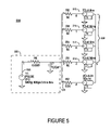
- FIG. 5 shows a representation 500 of a test system under calibration in accordance with an embodiment of the invention.
- Representation 500 shows examples of system values associated with the production of a composite waveform during calibration of a set of pins.
- An edge source 505 comprising a pulse generator 510 is used to generate a pulse with an amplitude of one volt, rise and fall times of 400 ps, pulse width of 3.6 ns, and a pulse period of 8 ns.
- the pulse width is much larger than the delays associated with the lines being calibrated.
- a set of lines 502 to be calibrated is shown.
- Each of lines 515 , 516 , 517 , and 518 have a characteristic impedance of 50 ohms and represent lines that may be individually selected for calibration.
- Line 520 represents a set of complementary lines and has a characteristic impedance of 0.01 ohms.
- Lines 515 , 516 , 517 , and 518 have delays of 0.8 ns, 0.85 ns, 0.9 ns, and 0.95 ns, respectively.
- Line 520 has a delay of 1.00 ns.
- Node 5 represents an input coupler that ties all of the lines together.
- the set of calibration lines 502 represent pretrigger values of 0.05 ns, 0.10 ns, 0.15 ns and 0.20 ns.
- FIG. 6 illustrates a response plot of the circuit representation of FIG. 5 in accordance with an embodiment of the invention.
- Plots V( 8 ), V( 7 ), V( 6 ), and v( 3 ) represent the composite waveform observed at nodes 8 , 7 , 6 , and 3 , respectively.
- Line 515 has the greatest delay difference with respect to the complementary lines 520 , and thus produces a composite waveform with a trough 605 that has the greatest depth.
- Line 518 has the smallest delay difference with respect to the complementary lines 520 and thus has the shallowest trough 610 .
- FIG. 7 shows a flowchart 700 for calibration of a set of input signal lines in an ATE system in accordance with an embodiment of the present invention.
- step 705 conventional TDR is performed to provide an initial alignment for the drivers associated with the signal lines. This step is optional and may be omitted. Generally, it is desirable that the delay difference of the initial alignment be less than about one third of the calibration edge used in the system.
- step 710 the input signal lines are coupled to each other.
- the input signal lines are not opened or coupled to ground. This coupling provides the physical configuration that is used to create the composite waveform that is used for calibration.
- a signal line is selected for calibration.
- the line under calibration will have an edge applied to it in advance of the edges applied to the remaining signal lines.
- a relative timing offset value is selected for the driver of the line under calibration.
- the initial value for the relative timing offset value is a pretrigger time value that is preferably one third to one half of the rise time of the calibration edge. Subsequent values may be obtained by incrementing or decrementing the initial value.
- a test signal is applied.
- the test signal includes a calibration edge applied to the line under calibration and a set of complementary edges applied to the remaining signal lines at a reference trigger time value.
- a reflected edge and the composite propagating towards the driver of the line under calibration are examined for a composite waveform trough (or other feature).
- the composite waveform is a superposition of a reflection of the calibration edge and the transmitted complementary edges.
- the composite waveform examination may be performed by a comparator managed by a controller.
- step 735 a check is made to see if a composite waveform trough exists, and whether its amplitude matches a predetermined value. If the observed trough amplitude does not match the predetermined value, then step 720 is executed. If there is a match, step 740 is executed.
- step 740 the current value for the relative timing offset is recorded or fixed for the driver of the line under calibration.
- step 745 a check is made to see if a relative timing offset value has been determined for each line in the set of input signal lines. If each line has not been calibrated, step 715 is executed. If each signal line has been calibrated, optional steps 750 to 770 may be performed.
- Optional steps 750 to 770 may be used to deskew the comparators coupled to the input signal lines. If the there is a significant difference among signal lines in the delay between the comparator and the signal source (driver), an unacceptable error may result. Deskewing accounts for the comparator/driver variation.
- step 750 a comparator/signal line is selected.
- step 755 the drivers on the other non-selected (complementary) lines are triggered to produce a combined edge.
- step 760 the time required for the comparator to detect the combined edge is measured.
- step 765 a check is made to see if each comparator/line has been selected. If not all line delays have been measured, step 750 is executed. If all line delays have been measured, step 770 is executed. In step 770 , the set of measurements may be used to adjust the timing of each of the drivers to offset the observed skew in the comparators.
- step 775 calibration is complete.
Landscapes
- Engineering & Computer Science (AREA)
- General Engineering & Computer Science (AREA)
- Physics & Mathematics (AREA)
- General Physics & Mathematics (AREA)
- Tests Of Electronic Circuits (AREA)
Abstract
Description
Claims (8)
Priority Applications (2)
| Application Number | Priority Date | Filing Date | Title |
|---|---|---|---|
| US10/729,800 US7009382B1 (en) | 2003-12-04 | 2003-12-04 | System and method for test socket calibration |
| US11/185,569 US7439728B1 (en) | 2003-12-04 | 2005-07-19 | System and method for test socket calibration using composite waveform |
Applications Claiming Priority (1)
| Application Number | Priority Date | Filing Date | Title |
|---|---|---|---|
| US10/729,800 US7009382B1 (en) | 2003-12-04 | 2003-12-04 | System and method for test socket calibration |
Related Child Applications (1)
| Application Number | Title | Priority Date | Filing Date |
|---|---|---|---|
| US11/185,569 Division US7439728B1 (en) | 2003-12-04 | 2005-07-19 | System and method for test socket calibration using composite waveform |
Publications (1)
| Publication Number | Publication Date |
|---|---|
| US7009382B1 true US7009382B1 (en) | 2006-03-07 |
Family
ID=35966252
Family Applications (2)
| Application Number | Title | Priority Date | Filing Date |
|---|---|---|---|
| US10/729,800 Expired - Lifetime US7009382B1 (en) | 2003-12-04 | 2003-12-04 | System and method for test socket calibration |
| US11/185,569 Expired - Fee Related US7439728B1 (en) | 2003-12-04 | 2005-07-19 | System and method for test socket calibration using composite waveform |
Family Applications After (1)
| Application Number | Title | Priority Date | Filing Date |
|---|---|---|---|
| US11/185,569 Expired - Fee Related US7439728B1 (en) | 2003-12-04 | 2005-07-19 | System and method for test socket calibration using composite waveform |
Country Status (1)
| Country | Link |
|---|---|
| US (2) | US7009382B1 (en) |
Cited By (2)
| Publication number | Priority date | Publication date | Assignee | Title |
|---|---|---|---|---|
| WO2010069349A1 (en) * | 2008-12-18 | 2010-06-24 | Verigy (Singapore) Pte Ltd. | Apparatus for determining a compensation parameter for compensating a signal level change of a test signal |
| US20190033372A1 (en) * | 2017-07-27 | 2019-01-31 | Teradyne, Inc. | Time-aligning communication channels |
Citations (4)
| Publication number | Priority date | Publication date | Assignee | Title |
|---|---|---|---|---|
| US5867030A (en) * | 1994-07-20 | 1999-02-02 | Advantest Corp. | Transmission path structure for measuring propagation delay time thereof |
| US6492797B1 (en) * | 2000-02-28 | 2002-12-10 | Schlumberger Technologies, Inc. | Socket calibration method and apparatus |
| US20030016041A1 (en) * | 2000-07-17 | 2003-01-23 | Mitsubishi Denki Kabushiki Kaisha | Method and apparatus for testing semiconductor integrated circuit, and semiconductor integrated circuit manufactured thereby |
| US6804620B1 (en) * | 2003-03-21 | 2004-10-12 | Advantest Corporation | Calibration method for system performance validation of automatic test equipment |
Family Cites Families (3)
| Publication number | Priority date | Publication date | Assignee | Title |
|---|---|---|---|---|
| JPH0862308A (en) * | 1994-08-22 | 1996-03-08 | Advantest Corp | Timing calibration method for measuring signal of semiconductor testing device and its circuit |
| TW557527B (en) * | 2001-03-26 | 2003-10-11 | Schlumberger Technologies Inc | Method and apparatus for calibration of integrated circuit tester timing |
| US6979996B2 (en) * | 2003-09-15 | 2005-12-27 | International Business Machines Corporation | Apparatus and method for automatic elimination of round-trip delay errors induced by automatic test equipment calibration |
-
2003
- 2003-12-04 US US10/729,800 patent/US7009382B1/en not_active Expired - Lifetime
-
2005
- 2005-07-19 US US11/185,569 patent/US7439728B1/en not_active Expired - Fee Related
Patent Citations (4)
| Publication number | Priority date | Publication date | Assignee | Title |
|---|---|---|---|---|
| US5867030A (en) * | 1994-07-20 | 1999-02-02 | Advantest Corp. | Transmission path structure for measuring propagation delay time thereof |
| US6492797B1 (en) * | 2000-02-28 | 2002-12-10 | Schlumberger Technologies, Inc. | Socket calibration method and apparatus |
| US20030016041A1 (en) * | 2000-07-17 | 2003-01-23 | Mitsubishi Denki Kabushiki Kaisha | Method and apparatus for testing semiconductor integrated circuit, and semiconductor integrated circuit manufactured thereby |
| US6804620B1 (en) * | 2003-03-21 | 2004-10-12 | Advantest Corporation | Calibration method for system performance validation of automatic test equipment |
Cited By (3)
| Publication number | Priority date | Publication date | Assignee | Title |
|---|---|---|---|---|
| WO2010069349A1 (en) * | 2008-12-18 | 2010-06-24 | Verigy (Singapore) Pte Ltd. | Apparatus for determining a compensation parameter for compensating a signal level change of a test signal |
| US20190033372A1 (en) * | 2017-07-27 | 2019-01-31 | Teradyne, Inc. | Time-aligning communication channels |
| US10564219B2 (en) * | 2017-07-27 | 2020-02-18 | Teradyne, Inc. | Time-aligning communication channels |
Also Published As
| Publication number | Publication date |
|---|---|
| US7439728B1 (en) | 2008-10-21 |
Similar Documents
| Publication | Publication Date | Title |
|---|---|---|
| US9164158B2 (en) | Calibration device | |
| US6911814B2 (en) | Apparatus and method for electromechanical testing and validation of probe cards | |
| US6622103B1 (en) | System for calibrating timing of an integrated circuit wafer tester | |
| JP4255284B2 (en) | Single-ended channel calibration for differential operation | |
| US5504432A (en) | System and method for detecting short, opens and connected pins on a printed circuit board using automatic test equipment | |
| TWI548889B (en) | Test equipment calibration | |
| US7120840B1 (en) | Method and system for improved ATE timing calibration at a device under test | |
| US6924651B2 (en) | Printed board inspecting apparatus | |
| SG184455A1 (en) | Apparatus and method for testing a plurality of devices under test | |
| US6794861B2 (en) | Method and apparatus for socket calibration of integrated circuit testers | |
| KR101329594B1 (en) | Calibration device | |
| CN108291929B (en) | Method and system for determining electrical path length | |
| US5256964A (en) | Tester calibration verification device | |
| US5867030A (en) | Transmission path structure for measuring propagation delay time thereof | |
| US6492797B1 (en) | Socket calibration method and apparatus | |
| US6812727B2 (en) | Semiconductor integrated circuit device and testing method thereof | |
| US7439728B1 (en) | System and method for test socket calibration using composite waveform | |
| CN107329103B (en) | Time transfer standard set of integrated circuit test system and test method thereof | |
| CN113504454A (en) | Calibration method of analyzer and chip test method and system | |
| US6831473B2 (en) | Ring calibration apparatus and method for automatic test equipment | |
| US6931346B2 (en) | Method and apparatus for reduced pin count package connection verification | |
| US8547082B2 (en) | Semiconductor device and pulse width detection method | |
| US20020158625A1 (en) | Test apparatus for parallel testing a number of electronic components and a method for calibrating the test apparatus | |
| JPH0210277A (en) | Circuit testing method and apparatus | |
| KR100577553B1 (en) | connecting unit for reliability test of semiconductor device test equipment and method for calibrating signal skew and jitter |
Legal Events
| Date | Code | Title | Description |
|---|---|---|---|
| AS | Assignment |
Owner name: NPTEST, INC., CALIFORNIA Free format text: ASSIGNMENT OF ASSIGNORS INTEREST;ASSIGNOR:HICKLING, ROBERT L.;REEL/FRAME:014777/0890 Effective date: 20031124 |
|
| AS | Assignment |
Owner name: CREDENCE SYSTEMS CORPORATION, CALIFORNIA Free format text: ASSIGNMENT OF ASSIGNORS INTEREST;ASSIGNOR:NPTEST, INC.;REEL/FRAME:015390/0777 Effective date: 20040713 |
|
| STCF | Information on status: patent grant |
Free format text: PATENTED CASE |
|
| FPAY | Fee payment |
Year of fee payment: 4 |
|
| FPAY | Fee payment |
Year of fee payment: 8 |
|
| AS | Assignment |
Owner name: SILICON VALLEY BANK, AS ADMINISTRATIVE AGENT, CALI Free format text: SECURITY AGREEMENT;ASSIGNORS:LTX-CREDENCE CORPORATION;EVERETT CHARLES TECHNOLOGIES LLC;REEL/FRAME:032086/0476 Effective date: 20131127 |
|
| AS | Assignment |
Owner name: XCERRA CORPORATION, MASSACHUSETTS Free format text: CHANGE OF NAME;ASSIGNOR:LTX-CREDENCE CORPORATION;REEL/FRAME:033032/0768 Effective date: 20140520 |
|
| AS | Assignment |
Owner name: SILICON VALLEY BANK, AS ADMINISTRATIVE AGENT, CALI Free format text: SECURITY AGREEMENT;ASSIGNORS:XCERRA CORPORATION;EVERETT CHARLES TECHNOLOGIES LLC;REEL/FRAME:034660/0188 Effective date: 20141215 Owner name: XCERRA CORPORATION, MASSACHUSETTS Free format text: RELEASE OF SECURITY INTEREST IN UNITED STATES PATENTS;ASSIGNOR:SILICON VALLEY BANK, AS ADMINISTRATIVE AGENT;REEL/FRAME:034660/0394 Effective date: 20141215 Owner name: EVERETT CHARLES TECHNOLOGIES LLC, MASSACHUSETTS Free format text: RELEASE OF SECURITY INTEREST IN UNITED STATES PATENTS;ASSIGNOR:SILICON VALLEY BANK, AS ADMINISTRATIVE AGENT;REEL/FRAME:034660/0394 Effective date: 20141215 |
|
| AS | Assignment |
Owner name: SILICON VALLEY BANK, AS ADMINISTRATIVE AGENT, CALI Free format text: CORRECTIVE ASSIGNMENT TO CORRECT THE INCORRECT PATENT NUMBER 7261561 AND REPLACE WITH PATENT NUMBER 7231561 PREVIOUSLY RECORDED ON REEL 034660 FRAME 0188. ASSIGNOR(S) HEREBY CONFIRMS THE SECURITY AGREEMENT;ASSIGNORS:XCERRA CORPORATION;EVERETT CHARLES TECHNOLOGIES LLC;REEL/FRAME:037824/0372 Effective date: 20141215 |
|
| MAFP | Maintenance fee payment |
Free format text: PAYMENT OF MAINTENANCE FEE, 12TH YEAR, LARGE ENTITY (ORIGINAL EVENT CODE: M1553) Year of fee payment: 12 |
|
| AS | Assignment |
Owner name: DEUTSCHE BANK AG NEW YORK BRANCH, AS COLLATERAL AGENT, NEW YORK Free format text: PATENT SECURITY AGREEMENT;ASSIGNOR:XCERRA CORPORATION;REEL/FRAME:047185/0624 Effective date: 20181001 Owner name: DEUTSCHE BANK AG NEW YORK BRANCH, AS COLLATERAL AG Free format text: PATENT SECURITY AGREEMENT;ASSIGNOR:XCERRA CORPORATION;REEL/FRAME:047185/0624 Effective date: 20181001 |
|
| AS | Assignment |
Owner name: DEUTSCHE BANK AG NEW YORK BRANCH, AS COLLATERAL AGENT, NEW YORK Free format text: CORRECTIVE ASSIGNMENT TO CORRECT THE INCORRECT STATEMENT THAT THIS DOCUMENT SERVES AS AN OATH/DECLARATION PREVIOUSLY RECORDED ON REEL 047185 FRAME 0628. ASSIGNOR(S) HEREBY CONFIRMS THE PATENT SECURITY AGREEMENT;ASSIGNOR:XCERRA CORPORATION;REEL/FRAME:047675/0354 Effective date: 20181001 Owner name: DEUTSCHE BANK AG NEW YORK BRANCH, AS COLLATERAL AG Free format text: CORRECTIVE ASSIGNMENT TO CORRECT THE INCORRECT STATEMENT THAT THIS DOCUMENT SERVES AS AN OATH/DECLARATION PREVIOUSLY RECORDED ON REEL 047185 FRAME 0628. ASSIGNOR(S) HEREBY CONFIRMS THE PATENT SECURITY AGREEMENT;ASSIGNOR:XCERRA CORPORATION;REEL/FRAME:047675/0354 Effective date: 20181001 |
|
| AS | Assignment |
Owner name: XCERRA CORPORATION, MASSACHUSETTS Free format text: TERMINATION AND RELEASE OF SECURITY INTEREST IN PATENTS, RECORDED AT REEL 047185, FRAME 0624;ASSIGNOR:DEUTSCHE BANK AG NEW YORK BRANCH, AS AGENT;REEL/FRAME:066762/0811 Effective date: 20240209 |