US7008853B1 - Method and system for fabricating free-standing nanostructures - Google Patents
Method and system for fabricating free-standing nanostructures Download PDFInfo
- Publication number
- US7008853B1 US7008853B1 US11/066,320 US6632005A US7008853B1 US 7008853 B1 US7008853 B1 US 7008853B1 US 6632005 A US6632005 A US 6632005A US 7008853 B1 US7008853 B1 US 7008853B1
- Authority
- US
- United States
- Prior art keywords
- semiconductor wafer
- process chamber
- carbon dioxide
- dioxide fluid
- etching
- Prior art date
- Legal status (The legal status is an assumption and is not a legal conclusion. Google has not performed a legal analysis and makes no representation as to the accuracy of the status listed.)
- Expired - Fee Related
Links
- 238000000034 method Methods 0.000 title claims abstract description 134
- 239000002086 nanomaterial Substances 0.000 title claims abstract description 34
- CURLTUGMZLYLDI-UHFFFAOYSA-N Carbon dioxide Chemical compound O=C=O CURLTUGMZLYLDI-UHFFFAOYSA-N 0.000 claims abstract description 120
- 238000005530 etching Methods 0.000 claims abstract description 79
- 239000004065 semiconductor Substances 0.000 claims abstract description 74
- 230000008569 process Effects 0.000 claims abstract description 72
- 229910002092 carbon dioxide Inorganic materials 0.000 claims abstract description 60
- 239000001569 carbon dioxide Substances 0.000 claims abstract description 60
- 239000012530 fluid Substances 0.000 claims abstract description 55
- 239000007788 liquid Substances 0.000 claims abstract description 25
- 238000013022 venting Methods 0.000 claims abstract description 9
- 239000003990 capacitor Substances 0.000 claims description 35
- 239000000758 substrate Substances 0.000 claims description 33
- 238000001035 drying Methods 0.000 claims description 20
- 239000006184 cosolvent Substances 0.000 claims description 11
- 239000000203 mixture Substances 0.000 claims description 11
- LFQSCWFLJHTTHZ-UHFFFAOYSA-N Ethanol Chemical compound CCO LFQSCWFLJHTTHZ-UHFFFAOYSA-N 0.000 claims description 10
- KRHYYFGTRYWZRS-UHFFFAOYSA-N Fluorane Chemical compound F KRHYYFGTRYWZRS-UHFFFAOYSA-N 0.000 claims description 9
- 239000000126 substance Substances 0.000 claims description 8
- YCKRFDGAMUMZLT-UHFFFAOYSA-N Fluorine atom Chemical compound [F] YCKRFDGAMUMZLT-UHFFFAOYSA-N 0.000 claims description 7
- 229910052731 fluorine Inorganic materials 0.000 claims description 7
- 239000011737 fluorine Substances 0.000 claims description 7
- OKKJLVBELUTLKV-UHFFFAOYSA-N Methanol Chemical compound OC OKKJLVBELUTLKV-UHFFFAOYSA-N 0.000 claims description 6
- LRHPLDYGYMQRHN-UHFFFAOYSA-N N-Butanol Chemical compound CCCCO LRHPLDYGYMQRHN-UHFFFAOYSA-N 0.000 claims description 6
- VYPSYNLAJGMNEJ-UHFFFAOYSA-N Silicium dioxide Chemical compound O=[Si]=O VYPSYNLAJGMNEJ-UHFFFAOYSA-N 0.000 claims description 6
- 150000001412 amines Chemical class 0.000 claims description 5
- 238000000151 deposition Methods 0.000 claims description 5
- KFZMGEQAYNKOFK-UHFFFAOYSA-N Isopropanol Chemical compound CC(C)O KFZMGEQAYNKOFK-UHFFFAOYSA-N 0.000 claims description 4
- AMQJEAYHLZJPGS-UHFFFAOYSA-N N-Pentanol Chemical compound CCCCCO AMQJEAYHLZJPGS-UHFFFAOYSA-N 0.000 claims description 4
- 150000001335 aliphatic alkanes Chemical class 0.000 claims description 4
- -1 di-glycol amine Chemical compound 0.000 claims description 4
- 238000011010 flushing procedure Methods 0.000 claims description 4
- 150000002576 ketones Chemical class 0.000 claims description 4
- 239000002736 nonionic surfactant Substances 0.000 claims description 4
- APSBXTVYXVQYAB-UHFFFAOYSA-M sodium docusate Chemical compound [Na+].CCCCC(CC)COC(=O)CC(S([O-])(=O)=O)C(=O)OCC(CC)CCCC APSBXTVYXVQYAB-UHFFFAOYSA-M 0.000 claims description 4
- NECRQCBKTGZNMH-UHFFFAOYSA-N 3,5-dimethylhex-1-yn-3-ol Chemical compound CC(C)CC(C)(O)C#C NECRQCBKTGZNMH-UHFFFAOYSA-N 0.000 claims description 3
- 239000003945 anionic surfactant Substances 0.000 claims description 3
- GPRLSGONYQIRFK-MNYXATJNSA-N triton Chemical compound [3H+] GPRLSGONYQIRFK-MNYXATJNSA-N 0.000 claims description 3
- DDFHBQSCUXNBSA-UHFFFAOYSA-N 5-(5-carboxythiophen-2-yl)thiophene-2-carboxylic acid Chemical compound S1C(C(=O)O)=CC=C1C1=CC=C(C(O)=O)S1 DDFHBQSCUXNBSA-UHFFFAOYSA-N 0.000 claims description 2
- IAYPIBMASNFSPL-UHFFFAOYSA-N Ethylene oxide Chemical compound C1CO1 IAYPIBMASNFSPL-UHFFFAOYSA-N 0.000 claims description 2
- SECXISVLQFMRJM-UHFFFAOYSA-N N-Methylpyrrolidone Chemical compound CN1CCCC1=O SECXISVLQFMRJM-UHFFFAOYSA-N 0.000 claims description 2
- UAOMVDZJSHZZME-UHFFFAOYSA-N diisopropylamine Chemical compound CC(C)NC(C)C UAOMVDZJSHZZME-UHFFFAOYSA-N 0.000 claims description 2
- 229960004592 isopropanol Drugs 0.000 claims description 2
- BDERNNFJNOPAEC-UHFFFAOYSA-N propan-1-ol Chemical compound CCCO BDERNNFJNOPAEC-UHFFFAOYSA-N 0.000 claims description 2
- 229910052814 silicon oxide Inorganic materials 0.000 claims description 2
- RKBCYCFRFCNLTO-UHFFFAOYSA-N triisopropylamine Chemical compound CC(C)N(C(C)C)C(C)C RKBCYCFRFCNLTO-UHFFFAOYSA-N 0.000 claims description 2
- 238000002347 injection Methods 0.000 claims 4
- 239000007924 injection Substances 0.000 claims 4
- 239000000243 solution Substances 0.000 claims 3
- 239000005368 silicate glass Substances 0.000 claims 1
- 235000012431 wafers Nutrition 0.000 description 48
- 238000012545 processing Methods 0.000 description 15
- 238000004140 cleaning Methods 0.000 description 11
- 239000000463 material Substances 0.000 description 9
- 239000012071 phase Substances 0.000 description 8
- 239000007789 gas Substances 0.000 description 7
- XUIMIQQOPSSXEZ-UHFFFAOYSA-N Silicon Chemical compound [Si] XUIMIQQOPSSXEZ-UHFFFAOYSA-N 0.000 description 5
- 238000005516 engineering process Methods 0.000 description 5
- 229910052710 silicon Inorganic materials 0.000 description 5
- 239000010703 silicon Substances 0.000 description 5
- 238000003860 storage Methods 0.000 description 4
- 239000004094 surface-active agent Substances 0.000 description 4
- 238000001039 wet etching Methods 0.000 description 4
- 230000007423 decrease Effects 0.000 description 3
- 230000008021 deposition Effects 0.000 description 3
- 238000009792 diffusion process Methods 0.000 description 3
- VLKZOEOYAKHREP-UHFFFAOYSA-N n-Hexane Chemical compound CCCCCC VLKZOEOYAKHREP-UHFFFAOYSA-N 0.000 description 3
- 239000002904 solvent Substances 0.000 description 3
- CSCPPACGZOOCGX-UHFFFAOYSA-N Acetone Chemical compound CC(C)=O CSCPPACGZOOCGX-UHFFFAOYSA-N 0.000 description 2
- 229910021417 amorphous silicon Inorganic materials 0.000 description 2
- 150000001875 compounds Chemical class 0.000 description 2
- 239000004020 conductor Substances 0.000 description 2
- 238000009472 formulation Methods 0.000 description 2
- 238000010348 incorporation Methods 0.000 description 2
- 238000004519 manufacturing process Methods 0.000 description 2
- 230000001404 mediated effect Effects 0.000 description 2
- 238000012986 modification Methods 0.000 description 2
- 230000004048 modification Effects 0.000 description 2
- 238000010587 phase diagram Methods 0.000 description 2
- 229960001866 silicon dioxide Drugs 0.000 description 2
- 235000012239 silicon dioxide Nutrition 0.000 description 2
- 239000000377 silicon dioxide Substances 0.000 description 2
- 238000012546 transfer Methods 0.000 description 2
- XLYOFNOQVPJJNP-UHFFFAOYSA-N water Substances O XLYOFNOQVPJJNP-UHFFFAOYSA-N 0.000 description 2
- 230000010062 adhesion mechanism Effects 0.000 description 1
- 230000002411 adverse Effects 0.000 description 1
- 229910052785 arsenic Inorganic materials 0.000 description 1
- RQNWIZPPADIBDY-UHFFFAOYSA-N arsenic atom Chemical compound [As] RQNWIZPPADIBDY-UHFFFAOYSA-N 0.000 description 1
- 230000004888 barrier function Effects 0.000 description 1
- 239000003795 chemical substances by application Substances 0.000 description 1
- 230000003247 decreasing effect Effects 0.000 description 1
- 239000008367 deionised water Substances 0.000 description 1
- 230000001627 detrimental effect Effects 0.000 description 1
- 239000007772 electrode material Substances 0.000 description 1
- 229910000040 hydrogen fluoride Inorganic materials 0.000 description 1
- 238000009413 insulation Methods 0.000 description 1
- 230000010354 integration Effects 0.000 description 1
- 238000011835 investigation Methods 0.000 description 1
- 238000002955 isolation Methods 0.000 description 1
- 239000007791 liquid phase Substances 0.000 description 1
- 231100000252 nontoxic Toxicity 0.000 description 1
- 230000003000 nontoxic effect Effects 0.000 description 1
- 238000001020 plasma etching Methods 0.000 description 1
- 238000005498 polishing Methods 0.000 description 1
- 239000011541 reaction mixture Substances 0.000 description 1
- 239000003440 toxic substance Substances 0.000 description 1
- WFKWXMTUELFFGS-UHFFFAOYSA-N tungsten Chemical compound [W] WFKWXMTUELFFGS-UHFFFAOYSA-N 0.000 description 1
- 229910052721 tungsten Inorganic materials 0.000 description 1
- 239000010937 tungsten Substances 0.000 description 1
Images


Classifications
-
- A—HUMAN NECESSITIES
- A61—MEDICAL OR VETERINARY SCIENCE; HYGIENE
- A61H—PHYSICAL THERAPY APPARATUS, e.g. DEVICES FOR LOCATING OR STIMULATING REFLEX POINTS IN THE BODY; ARTIFICIAL RESPIRATION; MASSAGE; BATHING DEVICES FOR SPECIAL THERAPEUTIC OR HYGIENIC PURPOSES OR SPECIFIC PARTS OF THE BODY
- A61H9/00—Pneumatic or hydraulic massage
- A61H9/005—Pneumatic massage
- A61H9/0078—Pneumatic massage with intermittent or alternately inflated bladders or cuffs
- A61H9/0092—Cuffs therefor
-
- H—ELECTRICITY
- H01—ELECTRIC ELEMENTS
- H01L—SEMICONDUCTOR DEVICES NOT COVERED BY CLASS H10
- H01L28/00—Passive two-terminal components without a potential-jump or surface barrier for integrated circuits; Details thereof; Multistep manufacturing processes therefor
- H01L28/40—Capacitors
- H01L28/60—Electrodes
- H01L28/82—Electrodes with an enlarged surface, e.g. formed by texturisation
- H01L28/90—Electrodes with an enlarged surface, e.g. formed by texturisation having vertical extensions
- H01L28/91—Electrodes with an enlarged surface, e.g. formed by texturisation having vertical extensions made by depositing layers, e.g. by depositing alternating conductive and insulating layers
-
- H—ELECTRICITY
- H01—ELECTRIC ELEMENTS
- H01L—SEMICONDUCTOR DEVICES NOT COVERED BY CLASS H10
- H01L21/00—Processes or apparatus adapted for the manufacture or treatment of semiconductor or solid state devices or of parts thereof
- H01L21/02—Manufacture or treatment of semiconductor devices or of parts thereof
- H01L21/04—Manufacture or treatment of semiconductor devices or of parts thereof the devices having potential barriers, e.g. a PN junction, depletion layer or carrier concentration layer
- H01L21/18—Manufacture or treatment of semiconductor devices or of parts thereof the devices having potential barriers, e.g. a PN junction, depletion layer or carrier concentration layer the devices having semiconductor bodies comprising elements of Group IV of the Periodic Table or AIIIBV compounds with or without impurities, e.g. doping materials
- H01L21/30—Treatment of semiconductor bodies using processes or apparatus not provided for in groups H01L21/20 - H01L21/26
- H01L21/31—Treatment of semiconductor bodies using processes or apparatus not provided for in groups H01L21/20 - H01L21/26 to form insulating layers thereon, e.g. for masking or by using photolithographic techniques; After treatment of these layers; Selection of materials for these layers
- H01L21/3105—After-treatment
- H01L21/311—Etching the insulating layers by chemical or physical means
- H01L21/31105—Etching inorganic layers
- H01L21/31111—Etching inorganic layers by chemical means
-
- H—ELECTRICITY
- H10—SEMICONDUCTOR DEVICES; ELECTRIC SOLID-STATE DEVICES NOT OTHERWISE PROVIDED FOR
- H10B—ELECTRONIC MEMORY DEVICES
- H10B12/00—Dynamic random access memory [DRAM] devices
- H10B12/01—Manufacture or treatment
- H10B12/02—Manufacture or treatment for one transistor one-capacitor [1T-1C] memory cells
- H10B12/03—Making the capacitor or connections thereto
- H10B12/033—Making the capacitor or connections thereto the capacitor extending over the transistor
-
- A—HUMAN NECESSITIES
- A61—MEDICAL OR VETERINARY SCIENCE; HYGIENE
- A61H—PHYSICAL THERAPY APPARATUS, e.g. DEVICES FOR LOCATING OR STIMULATING REFLEX POINTS IN THE BODY; ARTIFICIAL RESPIRATION; MASSAGE; BATHING DEVICES FOR SPECIAL THERAPEUTIC OR HYGIENIC PURPOSES OR SPECIFIC PARTS OF THE BODY
- A61H2201/00—Characteristics of apparatus not provided for in the preceding codes
- A61H2201/01—Constructive details
- A61H2201/0103—Constructive details inflatable
-
- A—HUMAN NECESSITIES
- A61—MEDICAL OR VETERINARY SCIENCE; HYGIENE
- A61H—PHYSICAL THERAPY APPARATUS, e.g. DEVICES FOR LOCATING OR STIMULATING REFLEX POINTS IN THE BODY; ARTIFICIAL RESPIRATION; MASSAGE; BATHING DEVICES FOR SPECIAL THERAPEUTIC OR HYGIENIC PURPOSES OR SPECIFIC PARTS OF THE BODY
- A61H2201/00—Characteristics of apparatus not provided for in the preceding codes
- A61H2201/12—Driving means
- A61H2201/1238—Driving means with hydraulic or pneumatic drive
Definitions
- the invention relates to systems and corresponding methods for fabricating free-standing nano-structures on a semiconductor wafer.
- the invention relates to the field of etching, cleaning, and drying a semiconductor wafer with a patterned layer to fabricate bottom electrode structures on a semiconductor wafer and to cleaning and/or drying the bottom electrode structures.
- DRAM dynamic random access memory cells
- the capacity of the storage capacitor also decreases.
- a certain minimum capacity typically on the order of about 30 femto farad
- the capacity of the storage capacitor is too small, the charge stored in the storage capacitor is not sufficient to produce a detectable signal. In such a case, the information stored in the memory cell is lost and the memory cell is not operating in a desired manner.
- one method introduces deep trench capacitors which are formed in the substrate of a semiconductor wafer to maintain a large capacitor area with a high capacity while using only a small amount of the surface of the substrate.
- the selection or access transistor is usually formed on the planar surface of the substrate in this method.
- stacked capacitors are used which are formed on top of a planar surface on the substrate.
- the selection transistors are formed below the planar surface in this method.
- the stacked capacitor includes a first electrode and a second electrode with a dielectric layer between the two electrodes.
- the first electrode also called bottom electrode
- the first electrode is usually formed as a cylindrical structure on the surface of the substrate by lining trenches of a patterned sacrificial mold layer with the electrode material. Afterwards, the bottom electrodes are released by etching the sacrificial mold layer. Subsequently, the surface of the bottom electrodes are cleaned to be prepared for further processing, including deposition of the dielectric layer and the second or top electrode.
- Etching and/or cleaning steps are usually performed by wet processing.
- Standard wet processing e.g. rinsing the wafer with ultra pure de-ionized water for cleaning purposes, introduces capillary forces between neighboring structures (e.g., between adjacent bottom electrodes). With reduced feature sizes, this may lead to adhesion of neighboring structures.
- This is described in Legtenberg et al., “ Stiction of surface macromachined structures after rinsing and drying: model and investigation of adhesion mechanisms”, Sensors and Actuators A, 43 (1994), pages 230–238. Adhesion of neighboring structures is mediated by the cleaning liquid, usually referred to as “stiction”.
- stiction is primarily important during drying steps which usually follow the etching and cleaning steps in semiconductor wafer processing.
- capillary forces induced by the liquid lead to adhesion of adjacent bottom electrodes.
- the adjacent bottom electrodes remain stuck to each other even after being completely dried, particularly when the adhesion force between the contacting adjacent bottom electrodes is larger than the elastic restoring force of the deformed bottom electrodes.
- Exposing wafers to an air-liquid interface during transfer between etching, cleaning and drying process modules is detrimental to obtaining stiction free process performance. Failing to achieve stiction free process performance ultimately results in a low yield of the produced circuits.
- One potential solution to this problem is to completely avoid wet processing and perform etching steps using gas phase processing, e.g. in a hydrogen fluoride vapor.
- gas phase processing leads to etching residues and to silicon surface termination states which in turn hinders further processing.
- a method for fabricating free-standing nanostructures includes: providing a semiconductor wafer including a substrate and a patterned layer above the substrate, the patterned layer comprising a plurality of openings ranging from the surface of the patterned layer to the surface of the substrate and structural elements being arranged within the openings, providing a process chamber, the process chamber being conFig.d to accommodate the semiconductor wafer, introducing the semiconductor wafer into the process chamber, injecting an etching chemistry into the process chamber to etch the patterned layer and to release the structural elements as free-standing nanostructures on the semiconductor wafer, the etching chemistry comprising a carbon dioxide fluid and an etching solution, rinsing the semiconductor wafer by flooding a carbon dioxide fluid into the process chamber, and drying the semiconductor wafer by injecting a supercritical carbon dioxide fluid into the process chamber and by venting out the supercritical carbon dioxide fluid from the process chamber.
- stiction free processing is achieved by employing unique properties of carbon dioxide in the supercritical or liquid state.
- the supercritical state is a high density phase characterized by a low viscosity and a zero surface tension, thus enabling better solubility and efficiency of the etching chemistry.
- properties similar to a gas phase presents high diffusion capabilities, allowing for easy solvent removal and greater drying efficiency.
- Another feature of the invention is that all process steps are performed in the same process chamber. This ensures that no air-liquid interfaces during transfer between etching, cleaning and drying process modules can occur. Accordingly, capillary forces are eliminated. This is achieved by employing carbon dioxide in its various states, i.e. supercritical, liquid and gas.
- a system for fabricating free-standing nanostructures comprises: a semiconductor wafer including a substrate and a patterned layer above the substrate, the patterned layer comprising a plurality of openings ranging from the surface of the patterned layer to the surface of the substrate and structural elements being arranged within the openings, a process chamber, the process chamber being conFig.d to accommodate the semiconductor wafer, means for introducing the semiconductor wafer into the process chamber, means for injecting an etching chemistry into the process chamber to etch the patterned layer and to release the structural elements as free-standing nanostructures on the semiconductor wafer, the etching chemistry comprising a liquid or supercritical carbon dioxide and an etching solution, means for rinsing the semiconductor wafer by flooding a liquid or supercritical carbon dioxide fluid into the process chamber, and means for drying the semiconductor wafer by venting out the supercritical carbon dioxide fluid from the process chamber.
- FIG. 1 depicts a side view in partial cross-section of a semiconductor wafer including a plurality of stacked capacitor DRAM-cells.
- FIG. 2 depicts a side view in partial cross-section of a semiconductor wafer including a plurality of surrounding gate transistors.
- FIGS. 3A–3D depict a side view in partial cross-section of parts of a stacked capacitor DRAM-cell formed in accordance with an exemplary method of the invention.
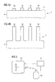
- FIGS. 4A–4B depict a side view in partial cross-section of free-standing nano-structures formed in accordance with another exemplary method of the invention.
- FIG. 5 depicts a side view in partial cross-section of a wafer drying, rinsing and cleaning system in accordance with the invention
- FIGS. 6A–6B are images showing a plurality of bottom electrodes of stacked capacitor DRAM-cells formed according to conventional wet etching techniques
- FIG. 7 is an image showing parts of a plurality of surrounding gate transistors formed according to conventional wet etching techniques.
- FIG. 8 is a flow chart of method steps for a further embodiment of the invention.
- FIG. 1 stacked capacitor DRAM-cells are shown in a side view. It should be appreciated that FIG. 1 merely serves as an illustration of fabricating stacked capacitor DRAM-cells, and the individual components shown in FIG. 1 are not true to scale.
- a semiconductor wafer 2 including a substrate 4 of semi-conductive material (e.g., silicon).
- the semiconductor wafer 2 is used for fabricating a plurality of stacked capacitor DRAM cells 6 .
- Each DRAM cell 6 includes a selection transistor 10 and a stacked capacitor 12 .
- the stacked capacitor 12 is located above the substrate surface 8 .
- the transistor 10 is located in the substrate 4 .
- the transistor 10 is formed by a first junction 14 and a second junction 16 .
- a gate 20 is disposed above a gate dielectric layer 18 .
- the gate 20 can include a stack of several layers (e.g., silicon and tungsten). The stack of several layers reduces the resistance of the gate 20 .
- the gate 20 also serves as a word line for addressing a specific DRAM cell 6 of the plurality of DRAM cells during operation.
- the first junction 14 is connected to a bit-line contact 22 .
- the bit-line contact 22 is disposed above the first junction 14 .
- the bit-line contact 22 is connected to a bit-line 24 which is located above the bit-line contact 22 .
- the bit-line 24 serves as a write or read line during operation.
- the second junction 16 is connected to a contact plug 26 .
- the contact plug 26 is disposed above the second junction 16 .
- the contact plug 26 serves as a connection to a bottom electrode 28 of the capacitor 12 .
- the bottom electrode 28 of the capacitor 12 is located above the substrate surface 8 .
- the bottom electrodes 28 are shown in a cross sectional side view.
- many different geometries can be used including cylindrical, elliptical or rectangular.
- the bottom electrode 28 is formed with vertical side walls above the contact plug 26 .
- non-vertical side walls or side walls being laterally recessed are also conceivable.
- the bottom electrode 28 of the capacitor 12 is covered by a dielectric layer 30 which serves as the dielectric of capacitor 12 .
- a top electrode 32 is disposed above the dielectric layer 30 .
- the top electrode 32 of the capacitor 12 is usually common to all DRAM cells 6 thus providing a connection between adjacent DRAM cells 6 .
- an isolation material can be disposed around the contact plugs 26 to avoid shorts to adjacent DRAM cells 6 . It is also possible to dispose the bit-line 24 on top of the top electrode 32 of the capacitor 12 by using a modified bit-line contact 22 .
- a second semiconductor wafer 2 including a substrate 4 of semi-conductive material (e.g., silicon).
- the semiconductor wafer 2 is used for fabricating a plurality of surrounding gate transistors 10 .
- Each transistor 10 is located on pillars 21 formed on the substrate 4 , where the transistor is formed by a first junction 14 on the lower side of the pillar 21 and a second junction 16 on the top side of the pillar 21 .
- a gate dielectric layer 18 and a gate 20 are disposed on the side walls of the pillar 21 between the first junction 14 and the second junction 16 .
- a semiconductor wafer 2 is first provided as shown in FIG. 3A .
- the semiconductor wafer 2 has the substrate 4 , with transistors 10 in the substrate (not shown) that have been formed for each DRAM cell 6 .
- contact plugs 26 are shown on the surface 8 of the substrate 4 .
- the contact plugs 26 are used to contact the bottom electrodes with the junction regions of the transistors.
- the contact plugs 26 usually have a low resistance and are made of, e.g., arsenic doped amorphous silicon.
- adjacent contact plugs 26 are spaced from each other at a distance ranging from 50 nm to 200 nm.
- a hard mask 40 as is deposited a mold layer.
- the hard mask 40 may be composed of, e.g. silicon oxide.
- the hard mask 40 serves later as a mold for the bottom electrode 28 of the stacked capacitor DRAM cell 6 . Accordingly, the thickness 41 of the hard mask directly affects the height of the bottom electrode 28 to be formed and, as a consequence, the capacitance of stacked capacitor 12 . Accordingly, the hard mask 40 must have a certain thickness which can be about 2 ⁇ m, e.g., for the 70 nm technology. However, other values for the thickness 41 might also be used, e.g., thicknesses in the range of 1 ⁇ m to 20 ⁇ m.
- a plurality of openings or trenches 48 are formed in the mask layer 40 , as shown in FIG. 3B .
- a photo lithographic patterned resist can be applied, e.g., to define the regions of the trenches 48 .
- Each trench 48 is arranged above a respective contact plug 26 , as shown in FIG. 3B .
- the trenches 48 are formed using a reactive ion etching step.
- trench 48 is formed from the top surface of the contact plugs 26 .
- the bottom of the trenches 48 are formed by the contact plugs 26 while the side walls 49 of the trench are formed within hard mask 40 .
- Etching of trenches 48 preferably leads to side walls 49 which have a width in the range of 50 nm to 200 nm as measured at the center of the trench 48 .
- a conductive layer 50 is conformably deposited on the semiconductor wafer 2 .
- the conductive layer 50 covers the top side of the hard mask 40 , the trench side walls 49 , and the bottom part of the trench 48 , (including the contact plugs 26 ).
- a suitable material for forming the conductive layer 50 by deposition can be, e.g., doped amorphous silicon.
- the conductive layer 50 serves later as the bottom electrode 28 of the stacked capacitor 12 of DRAM cell 6 once the hard mask 40 has been removed and the bottom electrodes are released. Therefore, the thickness of the conductive layer 50 affects the stability of the free-standing bottom electrodes 28 .
- a portion of the conductive layer 50 is removed from the surface of the hard mask 40 , as shown in FIG. 3C .
- This portion of the conductive layer 50 can be removed, e.g., by etching using a plasma etcher.
- the trenches 48 can be filled with a fill material, followed by removing the portion of the conductive layer 50 from the top surface of the hard mask 40 by chemical mechanical polishing, and then removing the fill material from within the trenches 48 .
- the fill material protects the inner sides of the trenches 48 from residues which could be a problem during later process steps (e.g., deposition of the dielectric layer 30 ).
- the next process step includes removing the hard mask layer 40 in order to release the remaining part of conductive layer 50 as free-standing nanostructures.
- the free-standing nanostructures form bottom electrodes of a stacked capacitor DRAM-cell 6 , as described above and depicted in FIG. 1 .
- FIGS. 4A and 4B another process sequence of fabricating free-standing nanostructures in accordance with the invention is shown.
- the surface 8 of semiconductor wafer 2 is covered with a patterned resist layer or any other suitable hard mask layer which has been structured by, e.g., a photo lithographic process step.
- the next process step includes releasing free-standing nanostructures 52 by etching.
- the free-standing nanostructures 52 of FIG. 4B are used as silicon pillars for surrounding gate transistors, such as the gate transistors described above and depicted in FIG. 2 .
- both releasing of the free-standing pillars and the bottom electrodes are performed by an etching step.
- the etching step employs an etching chemistry with a carbon dioxide fluid being in the liquid phase and an etching solution.
- the carbon dioxide fluid acts as a carrier for an etching solution which is chosen with respect to the material to be removed during the etching step.
- the mold layer can be composed of silicon-dioxide, such that a fluorine based etching chemistry (e.g., a formulation of a hydrofluoric acid) can be used to etch the mold layer.
- the etching chemistry is a mixture of carbon dioxide, the etching solution and a co-solvent.
- a co-solvent an alcohol/de-ionized water-mixture can be chosen, but alcohol, alkane, ketone, amine or fluorine containing mixtures can be used as well. Suitable substances are specified below.
- a surfactant can be incorporated in the etching chemistry in order to enhance water incorporation.
- the surfactant should be compatible with the carbon dioxide fluid.
- suitable substances are specified below.
- the process steps to release the free-standing structures are performed by an etching step mediated by a supercritical carbon dioxide fluid.
- a supercritical fluid are compounds above the so-called critical point in the pressure/temperature phase diagram at a certain critical temperature and critical pressure.
- the supercritical state is often called the fourth state of matter.
- Supercritical fluids exhibit properties of both liquids and fluids. For example, transport properties like viscosity are similar to gases while solvating properties like density are similar to those of liquids.
- a system is provided, as shown in FIG. 5 , that includes a process chamber 60 .
- the process chamber 60 is configured (e.g., suitably dimensioned) to accommodate the semiconductor wafer 2 .
- the process chamber 60 is connected to a reservoir 62 capable of delivering carbon dioxide in the supercritical phase.
- the system shown in FIG. 5 allows for adding extra substances with controlled concentrations, such as etching agents and/or co-solvents, as described below.
- the process chamber 60 can be pressurized and is operated with a controlled temperature. This is achieved by a control unit 64 , which is schematically connected to reservoir 62 and process chamber 60 .
- the semiconductor wafer 2 is introduced into the process chamber 60 .
- an etching chemistry is injected into the process chamber 60 .
- the etching chemistry is used to etch the hard mask layer 40 and to release the structural elements 52 as free-standing nanostructures on the semiconductor wafer 2 .
- the etching chemistry includes the supercritical or liquid carbon dioxide fluid and an etching solution.
- the etching solution is chosen with respect to the material to be removed during the etching step.
- the hard mask layer 40 or mold layer is composed of silicon-dioxide. Accordingly, a fluorine based etching chemistry might be used.
- the etching chemistry can be a formulation of a hydrofluoric acid in mixture of carbon dioxide and a co-solvent.
- the hydrofluoric acid is added to the etching chemistry on the level of a few micro-liter per liter of the etching chemistry.
- an alcohol/de-ionized water-mixture can be chosen, but alcohol, alkane (e.g., hexane), ketone (e.g., acetone), amine and/or fluorine containing mixtures can be used as well.
- Suitable alcohol substances include methanol, ethanol, propanol, iso-propanol, butanol and/or pentanol.
- Suitable amine substances include n-methylpyrrolidone, di-glycol amine, di-isopropyl amine and/or tri-isopropyl amine.
- Suitable fluorine containing substances include ammonium fluoride and/or 1,1,1-fluoro methane.
- a surfactant can be incorporated in the etching chemistry in order to enhance water incorporation.
- the surfactant should be compatible with the supercritical carbon dioxide fluid.
- An anionic surfactant as aerosol-OT or aerosol-OT derivatives and/or a non-ionic surfactant can be used.
- Suitable non-ionic surfactants include ethylene oxide and/or any one or combination of those commercially available compounds, and their derivatives, corresponding with the following trademarks: TRITON, SURFYNOL and DYNOL.
- the etching chemistry containing the supercritical carbon dioxide fluid and the etching solution is injected at a temperature and pressure above the critical point of carbon dioxide, which is located above about 34° C. and about 1050 psi in the phase diagram.
- the etching chemistry is injected into the process chamber 60 at a single transparent phase in a temperature and pressure range selected between 50° C. and 100° C. and at about 1100 psi.
- the supercritical state is further characterized by a low viscosity and negligible zero surface tension.
- the semiconductor wafer 2 When injecting the etching chemistry in the process chamber, the semiconductor wafer 2 is etched. As a result, the mold layer 40 is completely removed from the surface 8 of the semiconductor wafer 2 . The bottom electrodes 28 are released as free-standing nanostructures 52 on the surface 8 of the semiconductor wafer 2 .
- the same process chamber can be used for processing the non-supercritical liquid carbon dioxide fluid as described above by selecting proper processing conditions, i.e. a temperature and pressure below the critical point of carbon dioxide.
- the semiconductor wafer 2 is rinsed in the next step. This is achieved by flooding a supercritical carbon dioxide fluid into the process chamber 60 . Flooding is performed with a controlled gradient of flow of the supercritical carbon dioxide fluid which ensures that the etching chemistry is progressively removed from the reaction mixture.
- an optional flushing of the free-standing nanostructures is performed within the process chamber 60 .
- a supercritical carbon dioxide fluid is used.
- both the rinse step and the flushing step can also be performed with non-supercritical liquid carbon dioxide fluid.
- the same process chamber 60 is used for performing the etching, rinse and flushing steps by selecting proper processing conditions, i.e. a temperature and pressure above or below the critical point of the carbon dioxide fluid.
- a drying step of the semiconductor wafer is performed. This is achieved by venting out supercritical or liquid carbon dioxide fluid from the process chamber 60 . During this step the pressure created by the venting supercritical carbon dioxide fluid within the process chamber is released. Since the supercritical carbon dioxide fluid has negligible surface tension properties, capillary forces do not occur during drying. Accordingly, the process sequence according to this embodiment of the invention is free of stiction.
- stiction free processing is achieved by employing unique properties of carbon dioxide in the supercritical state and/or liquid state.
- the supercritical state is a high density phase characterized by a low viscosity and a zero surface tension, thus enabling better solubility and efficiency of the etching chemistry.
- the gas phase presents high diffusion capabilities, allowing for easy solvent removal and greater drying efficiency.
- Another feature of the embodiment of the invention is that the process is run entirely in the same process chamber 60 , ensuring that the nanostructures remain permanently wetted, and thus eliminating all together capillary forces. This is possible by making good use of the carbon dioxide various states, i.e. supercritical, liquid and gas.
- the process sequence according to the invention also offers additional advantages as carbon dioxide is a non-flammable and non-toxic substance and can easily be recycled.
- FIGS. 6A and 6B bottom electrodes 28 of stacked capacitor DRAM-cells are shown which are fabricated by applying prior art wet etching and drying techniques.
- a first SEM-picture 80 shows bottom electrodes 28 of stacked capacitor DRAM-cells in a side view.
- a second SEM-picture 82 shows bottom electrodes 28 of stacked capacitor DRAM-cells in a top view. Stiction between the neighboring cylinders of bottom electrodes 28 is clearly visible in the first SEM-picture 80 and in the second SEM-picture 82 .
- FIG. 7 free-standing nanostructures 52 of surrounding gate transistors are shown which are fabricated by applying prior art wet etching and drying techniques.
- a third SEM-picture 84 shows nanostructures 52 in a side view. Stiction between the neighboring nanostructures 52 is clearly visible in the third SEM-picture 84 .
- a semiconductor wafer 2 is provided in step 100 .
- a process chamber 60 is provided, which is configured to accommodate the semiconductor wafer 2 .
- the semiconductor wafer 2 is introduced into the process chamber 60 .
- an etching chemistry is injected into the process chamber 60 to etch the patterned layer 40 and to release free-standing nanostructures on the semiconductor wafer 2 .
- the etching chemistry includes a supercritical or liquid carbon dioxide fluid and an etching solution.
- step 108 the semiconductor wafer is rinsed by flooding a supercritical or liquid carbon dioxide fluid into the process chamber 60 .
- the semiconductor wafer 2 is dried by injecting a supercritical carbon dioxide fluid into the process chamber 60 and by venting out the supercritical carbon dioxide fluid from the process chamber 60 .
Landscapes
- Engineering & Computer Science (AREA)
- Power Engineering (AREA)
- Microelectronics & Electronic Packaging (AREA)
- Chemical & Material Sciences (AREA)
- Manufacturing & Machinery (AREA)
- Computer Hardware Design (AREA)
- Health & Medical Sciences (AREA)
- General Physics & Mathematics (AREA)
- Condensed Matter Physics & Semiconductors (AREA)
- Physics & Mathematics (AREA)
- Inorganic Chemistry (AREA)
- General Chemical & Material Sciences (AREA)
- Chemical Kinetics & Catalysis (AREA)
- Pain & Pain Management (AREA)
- Veterinary Medicine (AREA)
- Public Health (AREA)
- General Health & Medical Sciences (AREA)
- Animal Behavior & Ethology (AREA)
- Life Sciences & Earth Sciences (AREA)
- Rehabilitation Therapy (AREA)
- Physical Education & Sports Medicine (AREA)
- Epidemiology (AREA)
- Cleaning Or Drying Semiconductors (AREA)
- Weting (AREA)
- Semiconductor Memories (AREA)
- Drying Of Solid Materials (AREA)
Abstract
Description
| Reference numerals: |
| 2 | |
| 4 | |
| 6 | |
| 8 | |
| 10 | |
| 12 | |
| 14 | |
| 16 | |
| 18 | gate dielectric layer |
| 19 | |
| 20 | |
| 22 | |
| 24 | |
| 26 | |
| 28 | |
| 30 | |
| 32 | |
| 40 | |
| 41 | width of |
| 48 | |
| 49 | |
| 50 | |
| 52 | free-standing nano- |
| 60 | |
| 62 | |
| 64 | |
| 80 | |
| 82 | |
| 84 | |
| 100–110 | process steps |
Claims (32)
Priority Applications (6)
| Application Number | Priority Date | Filing Date | Title |
|---|---|---|---|
| US11/066,320 US7008853B1 (en) | 2005-02-25 | 2005-02-25 | Method and system for fabricating free-standing nanostructures |
| US11/325,631 US20060194404A1 (en) | 2005-02-25 | 2006-01-05 | Method and system for fabricating and cleaning free-standing nanostructures |
| TW095101977A TWI281198B (en) | 2005-02-25 | 2006-01-18 | Method and system for fabricating free-standing nanostructures |
| KR1020060018457A KR100810808B1 (en) | 2005-02-25 | 2006-02-24 | Method and system for fabricating free-standing nanostructures |
| CNA2006100592264A CN1825538A (en) | 2005-02-25 | 2006-02-24 | Method and system for fabricating free-standing nanostructures |
| JP2006050772A JP2006237620A (en) | 2005-02-25 | 2006-02-27 | Method of manufacturing self-supporting type nano structure part and its system |
Applications Claiming Priority (1)
| Application Number | Priority Date | Filing Date | Title |
|---|---|---|---|
| US11/066,320 US7008853B1 (en) | 2005-02-25 | 2005-02-25 | Method and system for fabricating free-standing nanostructures |
Related Child Applications (1)
| Application Number | Title | Priority Date | Filing Date |
|---|---|---|---|
| US11/325,631 Continuation-In-Part US20060194404A1 (en) | 2005-02-25 | 2006-01-05 | Method and system for fabricating and cleaning free-standing nanostructures |
Publications (1)
| Publication Number | Publication Date |
|---|---|
| US7008853B1 true US7008853B1 (en) | 2006-03-07 |
Family
ID=35966215
Family Applications (2)
| Application Number | Title | Priority Date | Filing Date |
|---|---|---|---|
| US11/066,320 Expired - Fee Related US7008853B1 (en) | 2005-02-25 | 2005-02-25 | Method and system for fabricating free-standing nanostructures |
| US11/325,631 Abandoned US20060194404A1 (en) | 2005-02-25 | 2006-01-05 | Method and system for fabricating and cleaning free-standing nanostructures |
Family Applications After (1)
| Application Number | Title | Priority Date | Filing Date |
|---|---|---|---|
| US11/325,631 Abandoned US20060194404A1 (en) | 2005-02-25 | 2006-01-05 | Method and system for fabricating and cleaning free-standing nanostructures |
Country Status (5)
| Country | Link |
|---|---|
| US (2) | US7008853B1 (en) |
| JP (1) | JP2006237620A (en) |
| KR (1) | KR100810808B1 (en) |
| CN (1) | CN1825538A (en) |
| TW (1) | TWI281198B (en) |
Cited By (8)
| Publication number | Priority date | Publication date | Assignee | Title |
|---|---|---|---|---|
| WO2007115849A1 (en) | 2006-04-03 | 2007-10-18 | Robert Bosch Gmbh | Method for treatment of material having nanoscale pores |
| US20080125342A1 (en) * | 2006-11-07 | 2008-05-29 | Advanced Technology Materials, Inc. | Formulations for cleaning memory device structures |
| US20080166878A1 (en) * | 2007-01-08 | 2008-07-10 | Sharp Laboratories Of America, Inc. | Silicon nanostructures and fabrication thereof |
| US20110049673A1 (en) * | 2009-08-26 | 2011-03-03 | International Business Machines Corporation | Nanopillar Decoupling Capacitor |
| US9027576B2 (en) | 2013-03-12 | 2015-05-12 | Samsung Electronics Co., Ltd. | Substrate treatment systems using supercritical fluid |
| RU2585322C2 (en) * | 2011-03-18 | 2016-05-27 | Басф Се | Method of producing integrated circuits, optical devices, micromachines and mechanical high-precision devices with layers of structured material with line spacing of 50 nm or less |
| US11094524B2 (en) | 2016-09-12 | 2021-08-17 | SCREEN Holdings Co., Ltd. | Substrate processing method and substrate processing apparatus |
| US20210287919A1 (en) * | 2020-03-16 | 2021-09-16 | Tokyo Electron Limited | System and Methods for Wafer Drying |
Families Citing this family (12)
| Publication number | Priority date | Publication date | Assignee | Title |
|---|---|---|---|---|
| US8084367B2 (en) * | 2006-05-24 | 2011-12-27 | Samsung Electronics Co., Ltd | Etching, cleaning and drying methods using supercritical fluid and chamber systems using these methods |
| US8153019B2 (en) | 2007-08-06 | 2012-04-10 | Micron Technology, Inc. | Methods for substantially equalizing rates at which material is removed over an area of a structure or film that includes recesses or crevices |
| US8153533B2 (en) * | 2008-09-24 | 2012-04-10 | Lam Research | Methods and systems for preventing feature collapse during microelectronic topography fabrication |
| US8961701B2 (en) * | 2008-09-24 | 2015-02-24 | Lam Research Corporation | Method and system of drying a microelectronic topography |
| US9620410B1 (en) * | 2009-01-20 | 2017-04-11 | Lam Research Corporation | Methods for preventing precipitation of etch byproducts during an etch process and/or subsequent rinse process |
| US20100184301A1 (en) * | 2009-01-20 | 2010-07-22 | Lam Research | Methods for Preventing Precipitation of Etch Byproducts During an Etch Process and/or Subsequent Rinse Process |
| US20110117752A1 (en) * | 2009-11-18 | 2011-05-19 | Kwon Taek Lim | Method and system for etching a silicon dioxide film using densified carbon dioxide |
| CN102299051B (en) * | 2010-06-25 | 2014-04-02 | 中国科学院微电子研究所 | Method and device for drying micro-electronic part |
| KR101329317B1 (en) * | 2011-12-07 | 2013-11-25 | 한국과학기술연구원 | Apparatus and method for drying substrate |
| KR101332306B1 (en) * | 2012-03-30 | 2013-11-22 | 한국기계연구원 | Method for manufacturing nano freestanding nano thin-film |
| JP6875811B2 (en) | 2016-09-16 | 2021-05-26 | 株式会社Screenホールディングス | Pattern collapse recovery method, board processing method and board processing equipment |
| US10796969B2 (en) * | 2018-09-07 | 2020-10-06 | Kla-Tencor Corporation | System and method for fabricating semiconductor wafer features having controlled dimensions |
Citations (1)
| Publication number | Priority date | Publication date | Assignee | Title |
|---|---|---|---|---|
| US20040003828A1 (en) * | 2002-03-21 | 2004-01-08 | Jackson David P. | Precision surface treatments using dense fluids and a plasma |
Family Cites Families (31)
| Publication number | Priority date | Publication date | Assignee | Title |
|---|---|---|---|---|
| JP2663483B2 (en) * | 1988-02-29 | 1997-10-15 | 勝 西川 | Method of forming resist pattern |
| US5013366A (en) * | 1988-12-07 | 1991-05-07 | Hughes Aircraft Company | Cleaning process using phase shifting of dense phase gases |
| JPH08330266A (en) * | 1995-05-31 | 1996-12-13 | Texas Instr Inc <Ti> | Method of cleansing and processing surface of semiconductor device or the like |
| JP3265340B2 (en) * | 1995-07-26 | 2002-03-11 | シャープ株式会社 | Resist removal method and resist stripper |
| US5783082A (en) * | 1995-11-03 | 1998-07-21 | University Of North Carolina | Cleaning process using carbon dioxide as a solvent and employing molecularly engineered surfactants |
| US5908510A (en) * | 1996-10-16 | 1999-06-01 | International Business Machines Corporation | Residue removal by supercritical fluids |
| US6149828A (en) * | 1997-05-05 | 2000-11-21 | Micron Technology, Inc. | Supercritical etching compositions and method of using same |
| US6306564B1 (en) * | 1997-05-27 | 2001-10-23 | Tokyo Electron Limited | Removal of resist or residue from semiconductors using supercritical carbon dioxide |
| US6500605B1 (en) * | 1997-05-27 | 2002-12-31 | Tokyo Electron Limited | Removal of photoresist and residue from substrate using supercritical carbon dioxide process |
| KR19990000357A (en) * | 1997-06-05 | 1999-01-15 | 윤종용 | Semiconductor manufacturing device |
| US6277753B1 (en) * | 1998-09-28 | 2001-08-21 | Supercritical Systems Inc. | Removal of CMP residue from semiconductors using supercritical carbon dioxide process |
| JP2000106358A (en) | 1998-09-29 | 2000-04-11 | Mitsubishi Electric Corp | Semiconductor manufacturing apparatus and method for processing semiconductor substrate |
| US6602349B2 (en) * | 1999-08-05 | 2003-08-05 | S.C. Fluids, Inc. | Supercritical fluid cleaning process for precision surfaces |
| US6286231B1 (en) * | 2000-01-12 | 2001-09-11 | Semitool, Inc. | Method and apparatus for high-pressure wafer processing and drying |
| US6558475B1 (en) * | 2000-04-10 | 2003-05-06 | International Business Machines Corporation | Process for cleaning a workpiece using supercritical carbon dioxide |
| US6562146B1 (en) * | 2001-02-15 | 2003-05-13 | Micell Technologies, Inc. | Processes for cleaning and drying microelectronic structures using liquid or supercritical carbon dioxide |
| US7189435B2 (en) * | 2001-03-14 | 2007-03-13 | University Of Massachusetts | Nanofabrication |
| US20030116176A1 (en) * | 2001-04-18 | 2003-06-26 | Rothman Laura B. | Supercritical fluid processes with megasonics |
| TW538472B (en) * | 2001-04-27 | 2003-06-21 | Kobe Steel Ltd | Method and system for processing substrate |
| JP4044300B2 (en) | 2001-04-27 | 2008-02-06 | 株式会社神戸製鋼所 | Wafer processing equipment and processing method |
| DE10160720A1 (en) * | 2001-12-11 | 2003-06-18 | Basf Ag | New water-soluble or -dispersible copolymer, useful in cosmetic products e.g. skin cleansers, prepared by polymerization of an N-vinyl lactam and a comonomer, and polymerization of an anionic monomer in the presence of the product |
| JP2003179026A (en) * | 2001-12-13 | 2003-06-27 | Hitachi Ltd | Method of manufacturing semiconductor device |
| AU2003217547A1 (en) * | 2002-02-15 | 2003-09-09 | Supercritical Systems Inc. | Drying resist with a solvent bath and supercritical co2 |
| CN101005024B (en) * | 2002-04-12 | 2011-06-08 | 东京毅力科创株式会社 | Method of treatment of porous dielectric films to reduce damage during cleaning |
| JP2004088095A (en) * | 2002-08-07 | 2004-03-18 | Sony Corp | Washing method |
| US20040118812A1 (en) * | 2002-08-09 | 2004-06-24 | Watkins James J. | Etch method using supercritical fluids |
| US20040134885A1 (en) * | 2003-01-14 | 2004-07-15 | Iyer Subramanyam A. | Etching and cleaning of semiconductors using supercritical carbon dioxide |
| JP2004225152A (en) * | 2003-01-27 | 2004-08-12 | Tokyo Electron Ltd | Method for treating substrate and method for manufacturing semiconductor device |
| JP2005150332A (en) * | 2003-11-14 | 2005-06-09 | Sony Corp | Etching method |
| KR100534103B1 (en) * | 2004-01-14 | 2005-12-06 | 삼성전자주식회사 | Method of fabricating a microelectronic device using supercritical fluid |
| US20060186088A1 (en) * | 2005-02-23 | 2006-08-24 | Gunilla Jacobson | Etching and cleaning BPSG material using supercritical processing |
-
2005
- 2005-02-25 US US11/066,320 patent/US7008853B1/en not_active Expired - Fee Related
-
2006
- 2006-01-05 US US11/325,631 patent/US20060194404A1/en not_active Abandoned
- 2006-01-18 TW TW095101977A patent/TWI281198B/en not_active IP Right Cessation
- 2006-02-24 KR KR1020060018457A patent/KR100810808B1/en not_active IP Right Cessation
- 2006-02-24 CN CNA2006100592264A patent/CN1825538A/en active Pending
- 2006-02-27 JP JP2006050772A patent/JP2006237620A/en active Pending
Patent Citations (1)
| Publication number | Priority date | Publication date | Assignee | Title |
|---|---|---|---|---|
| US20040003828A1 (en) * | 2002-03-21 | 2004-01-08 | Jackson David P. | Precision surface treatments using dense fluids and a plasma |
Non-Patent Citations (2)
| Title |
|---|
| Goldfarb D. et al., "Aqueous-Based Photoresist Drying Using Supercritical Carbon Dioxide to Prevent Pattern Collapse", J. Vac.Sci. Technol. B 18(6), Nov./Dec. 2000, pp. 3313-3317. |
| Legtenberg, R. et al.., "Stiction of Surface Macromachined Structures after Rinsing and Drying: Model and Investigation of Adhesion Mechanisms", Sensors and Actuators A, 43 (1994), pp. 230-238. |
Cited By (13)
| Publication number | Priority date | Publication date | Assignee | Title |
|---|---|---|---|---|
| WO2007115849A1 (en) | 2006-04-03 | 2007-10-18 | Robert Bosch Gmbh | Method for treatment of material having nanoscale pores |
| US20100009077A1 (en) * | 2006-04-03 | 2010-01-14 | Franz Laermer | Method for Treating a Material Having Nanoscale Pores |
| US20080125342A1 (en) * | 2006-11-07 | 2008-05-29 | Advanced Technology Materials, Inc. | Formulations for cleaning memory device structures |
| US20080166878A1 (en) * | 2007-01-08 | 2008-07-10 | Sharp Laboratories Of America, Inc. | Silicon nanostructures and fabrication thereof |
| US8680651B2 (en) | 2009-08-26 | 2014-03-25 | International Business Machines Corporation | Nanopillar decoupling capacitor |
| US8258037B2 (en) | 2009-08-26 | 2012-09-04 | International Business Machines Corporation | Nanopillar decoupling capacitor |
| US20110049673A1 (en) * | 2009-08-26 | 2011-03-03 | International Business Machines Corporation | Nanopillar Decoupling Capacitor |
| RU2585322C2 (en) * | 2011-03-18 | 2016-05-27 | Басф Се | Method of producing integrated circuits, optical devices, micromachines and mechanical high-precision devices with layers of structured material with line spacing of 50 nm or less |
| US9027576B2 (en) | 2013-03-12 | 2015-05-12 | Samsung Electronics Co., Ltd. | Substrate treatment systems using supercritical fluid |
| US11094524B2 (en) | 2016-09-12 | 2021-08-17 | SCREEN Holdings Co., Ltd. | Substrate processing method and substrate processing apparatus |
| US20210287919A1 (en) * | 2020-03-16 | 2021-09-16 | Tokyo Electron Limited | System and Methods for Wafer Drying |
| US11515178B2 (en) * | 2020-03-16 | 2022-11-29 | Tokyo Electron Limited | System and methods for wafer drying |
| US20230092779A1 (en) * | 2020-03-16 | 2023-03-23 | Tokyo Electron Limited | System and Methods for Wafer Drying |
Also Published As
| Publication number | Publication date |
|---|---|
| TW200633016A (en) | 2006-09-16 |
| CN1825538A (en) | 2006-08-30 |
| KR20060094925A (en) | 2006-08-30 |
| JP2006237620A (en) | 2006-09-07 |
| KR100810808B1 (en) | 2008-03-06 |
| US20060194404A1 (en) | 2006-08-31 |
| TWI281198B (en) | 2007-05-11 |
Similar Documents
| Publication | Publication Date | Title |
|---|---|---|
| US7008853B1 (en) | Method and system for fabricating free-standing nanostructures | |
| US6537870B1 (en) | Method of forming an integrated circuit comprising a self aligned trench | |
| US11651952B2 (en) | Using sacrificial polymer materials in semiconductor processing | |
| JP2009158913A (en) | Fine pattern forming method of semiconductor element | |
| US5985729A (en) | Method for manufacturing a capacitor of a trench DRAM cell | |
| US6188096B1 (en) | DRAM cell capacitor having increased trench capacitance | |
| US7579253B2 (en) | Method for cleaning a semiconductor wafer | |
| US7018893B1 (en) | Method for fabricating bottom electrodes of stacked capacitor memory cells | |
| CN114823539A (en) | Manufacturing method of semiconductor structure and semiconductor structure | |
| US6214686B1 (en) | Spatially offset deep trenches for high density DRAMS | |
| US20030045119A1 (en) | Method for forming a bottle-shaped trench | |
| US7115934B2 (en) | Method and structure for enhancing trench capacitance | |
| US11862513B2 (en) | Manufacturing method of semiconductor structure | |
| WO2022160629A1 (en) | Manufacturing method for semiconductor structure and semiconductor structure | |
| US11791152B2 (en) | Residue removal during semiconductor device formation | |
| CN113471148B (en) | Method for manufacturing semiconductor structure | |
| WO2021169797A1 (en) | Semiconductor structure preparation method and semiconductor structure | |
| US6236080B1 (en) | Method of manufacturing a capacitor for high density DRAMs | |
| US11997845B2 (en) | Method for manufacturing semiconductor structure and semiconductor structure | |
| US20220246617A1 (en) | Method for manufacturing semiconductor structure and semiconductor structure | |
| WO2024077951A1 (en) | Semiconductor structure, semiconductor structure manufacturing method, and memory manufacturing method | |
| US20220068937A1 (en) | Method for manufacturing memory and same | |
| KR100511001B1 (en) | Method for fabricating capacitor in semiconductor device | |
| KR100672756B1 (en) | Method for manufacturing capacitor in semiconductor device | |
| CN117673044A (en) | Semiconductor structure and manufacturing method thereof |
Legal Events
| Date | Code | Title | Description |
|---|---|---|---|
| AS | Assignment |
Owner name: INFINEON TECHNOLOGIES AG, GERMANY Free format text: ASSIGNMENT OF ASSIGNORS INTEREST;ASSIGNORS:DUPONT, AUDREY;HOYER, RONALD;REEL/FRAME:016772/0598 Effective date: 20050405 |
|
| FPAY | Fee payment |
Year of fee payment: 4 |
|
| AS | Assignment |
Owner name: QIMONDA AG, GERMANY Free format text: ASSIGNMENT OF ASSIGNORS INTEREST;ASSIGNOR:INFINEON TECHNOLOGIES AG;REEL/FRAME:023806/0001 Effective date: 20060425 Owner name: QIMONDA AG,GERMANY Free format text: ASSIGNMENT OF ASSIGNORS INTEREST;ASSIGNOR:INFINEON TECHNOLOGIES AG;REEL/FRAME:023806/0001 Effective date: 20060425 |
|
| FPAY | Fee payment |
Year of fee payment: 8 |
|
| AS | Assignment |
Owner name: INFINEON TECHNOLOGIES AG, GERMANY Free format text: ASSIGNMENT OF ASSIGNORS INTEREST;ASSIGNOR:QIMONDA AG;REEL/FRAME:035623/0001 Effective date: 20141009 |
|
| AS | Assignment |
Owner name: POLARIS INNOVATIONS LIMITED, IRELAND Free format text: ASSIGNMENT OF ASSIGNORS INTEREST;ASSIGNOR:INFINEON TECHNOLOGIES AG;REEL/FRAME:036908/0923 Effective date: 20150708 |
|
| FEPP | Fee payment procedure |
Free format text: MAINTENANCE FEE REMINDER MAILED (ORIGINAL EVENT CODE: REM.) |
|
| LAPS | Lapse for failure to pay maintenance fees |
Free format text: PATENT EXPIRED FOR FAILURE TO PAY MAINTENANCE FEES (ORIGINAL EVENT CODE: EXP.) |
|
| STCH | Information on status: patent discontinuation |
Free format text: PATENT EXPIRED DUE TO NONPAYMENT OF MAINTENANCE FEES UNDER 37 CFR 1.362 |
|
| FP | Lapsed due to failure to pay maintenance fee |
Effective date: 20180307 |