US6940436B2 - Analog-to-digital conversion system with second order noise shaping and a single amplifier - Google Patents
Analog-to-digital conversion system with second order noise shaping and a single amplifier Download PDFInfo
- Publication number
- US6940436B2 US6940436B2 US10/698,830 US69883003A US6940436B2 US 6940436 B2 US6940436 B2 US 6940436B2 US 69883003 A US69883003 A US 69883003A US 6940436 B2 US6940436 B2 US 6940436B2
- Authority
- US
- United States
- Prior art keywords
- digital
- analog
- converter
- dac
- integrator
- Prior art date
- Legal status (The legal status is an assumption and is not a legal conclusion. Google has not performed a legal analysis and makes no representation as to the accuracy of the status listed.)
- Expired - Lifetime
Links
- 238000007493 shaping process Methods 0.000 title claims abstract description 67
- 238000006243 chemical reaction Methods 0.000 title claims abstract description 39
- 238000013139 quantization Methods 0.000 claims abstract description 51
- 238000012545 processing Methods 0.000 claims abstract description 30
- 239000003990 capacitor Substances 0.000 claims description 51
- 230000003111 delayed effect Effects 0.000 claims description 6
- 238000004088 simulation Methods 0.000 description 22
- 238000005070 sampling Methods 0.000 description 15
- 238000012546 transfer Methods 0.000 description 15
- 238000013461 design Methods 0.000 description 10
- 229920005994 diacetyl cellulose Polymers 0.000 description 9
- 238000000034 method Methods 0.000 description 8
- 230000008569 process Effects 0.000 description 6
- 230000000694 effects Effects 0.000 description 3
- 238000001914 filtration Methods 0.000 description 3
- 238000012935 Averaging Methods 0.000 description 2
- 238000012952 Resampling Methods 0.000 description 2
- 238000013459 approach Methods 0.000 description 2
- 238000004891 communication Methods 0.000 description 2
- 238000010586 diagram Methods 0.000 description 2
- 239000007787 solid Substances 0.000 description 2
- 238000001228 spectrum Methods 0.000 description 2
- 101000634196 Homo sapiens Neurotrophin-3 Proteins 0.000 description 1
- 101001124017 Homo sapiens Nuclear transport factor 2 Proteins 0.000 description 1
- 101150036143 NTF3 gene Proteins 0.000 description 1
- 102100029268 Neurotrophin-3 Human genes 0.000 description 1
- 102100028418 Nuclear transport factor 2 Human genes 0.000 description 1
- 101100099288 Schizosaccharomyces pombe (strain 972 / ATCC 24843) thi1 gene Proteins 0.000 description 1
- 239000000654 additive Substances 0.000 description 1
- 230000000996 additive effect Effects 0.000 description 1
- 230000002411 adverse Effects 0.000 description 1
- 230000004075 alteration Effects 0.000 description 1
- 230000000712 assembly Effects 0.000 description 1
- 238000000429 assembly Methods 0.000 description 1
- 230000006399 behavior Effects 0.000 description 1
- 230000003542 behavioural effect Effects 0.000 description 1
- 239000000969 carrier Substances 0.000 description 1
- 230000000052 comparative effect Effects 0.000 description 1
- 230000008878 coupling Effects 0.000 description 1
- 238000010168 coupling process Methods 0.000 description 1
- 238000005859 coupling reaction Methods 0.000 description 1
- 230000003247 decreasing effect Effects 0.000 description 1
- 230000000593 degrading effect Effects 0.000 description 1
- 230000001419 dependent effect Effects 0.000 description 1
- 230000010354 integration Effects 0.000 description 1
- 238000004519 manufacturing process Methods 0.000 description 1
- 238000005259 measurement Methods 0.000 description 1
- 238000012986 modification Methods 0.000 description 1
- 230000004048 modification Effects 0.000 description 1
- 230000003071 parasitic effect Effects 0.000 description 1
- 230000009467 reduction Effects 0.000 description 1
Images


Classifications
-
- H—ELECTRICITY
- H03—ELECTRONIC CIRCUITRY
- H03M—CODING; DECODING; CODE CONVERSION IN GENERAL
- H03M3/00—Conversion of analogue values to or from differential modulation
- H03M3/30—Delta-sigma modulation
- H03M3/39—Structural details of delta-sigma modulators, e.g. incremental delta-sigma modulators
- H03M3/412—Structural details of delta-sigma modulators, e.g. incremental delta-sigma modulators characterised by the number of quantisers and their type and resolution
-
- H—ELECTRICITY
- H03—ELECTRONIC CIRCUITRY
- H03M—CODING; DECODING; CODE CONVERSION IN GENERAL
- H03M3/00—Conversion of analogue values to or from differential modulation
- H03M3/30—Delta-sigma modulation
- H03M3/39—Structural details of delta-sigma modulators, e.g. incremental delta-sigma modulators
- H03M3/436—Structural details of delta-sigma modulators, e.g. incremental delta-sigma modulators characterised by the order of the loop filter, e.g. error feedback type
- H03M3/456—Structural details of delta-sigma modulators, e.g. incremental delta-sigma modulators characterised by the order of the loop filter, e.g. error feedback type the modulator having a first order loop filter in the feedforward path
-
- H—ELECTRICITY
- H03—ELECTRONIC CIRCUITRY
- H03M—CODING; DECODING; CODE CONVERSION IN GENERAL
- H03M7/00—Conversion of a code where information is represented by a given sequence or number of digits to a code where the same, similar or subset of information is represented by a different sequence or number of digits
- H03M7/30—Compression; Expansion; Suppression of unnecessary data, e.g. redundancy reduction
- H03M7/3002—Conversion to or from differential modulation
- H03M7/3004—Digital delta-sigma modulation
- H03M7/3015—Structural details of digital delta-sigma modulators
- H03M7/3031—Structural details of digital delta-sigma modulators characterised by the order of the loop filter, e.g. having a first order loop filter in the feedforward path
- H03M7/3042—Structural details of digital delta-sigma modulators characterised by the order of the loop filter, e.g. having a first order loop filter in the feedforward path the modulator being of the error feedback type, i.e. having loop filter stages in the feedback path only
Definitions
- the present invention relates generally to data conversion systems and more particularly to a single amplifier analog-to-digital converter with second order noise shaping.
- Analog-to-digital (A/D) converters are electrical circuit devices that convert continuous signals, such as voltages or currents, from the analog domain to the digital domain where the signals are represented by numbers.
- Another type is known as a sigma delta or delta sigma (e.g., ⁇ - ⁇ ) A/D converter that includes a sigma delta modulator operating as a type of noise shaping encoder, typically with a 1–3 bit quantized digital output.
- Delta sigma e.g., ⁇ - ⁇
- sigma delta modulators are often used in mixed signal integrated A/D converters, because of their insensitivity to CMOS process linearity and matching problems when compared to other A/D converter types. These features make ⁇ - ⁇ based mixed signal solutions very attractive for a number of applications, such as audio, receiver channels of communication devices (wireless in particular), sensor interface circuits and measurement systems.
- Delta sigma converters are operated at a significantly higher sampling rate than the bandwidth of the analog input signal, a technique referred to as oversampling, wherein the analog input signal is sampled at a very high sampling rate in order to perform a noise shaping function.
- the oversampling is commonly performed at a multiple of the Nyquist rate (F N ) for a given input signal frequency content (e.g., sampling frequency F S is often 10 to 1000 times F N ), wherein quantization noise power is spread over a bandwidth equal to the sampling frequency.
- Noise shaping filters typically integrators, are commonly provided in the forward signal path of the delta sigma modulator. Digital filtering is performed on the oversampled digital output to achieve a high resolution, and decimation is employed to reduce the effective sampling rate back to the “Nyquist” rate.
- a conventional second order delta sigma modulator 2 is illustrated in FIG. 1 , comprising first and second analog adder/integrators 4 and 6 , respectively.
- the first adder/integrator 4 comprises a first summing junction 12 and a first integrator (e.g., low pass filter) 16
- the second adder/integrator 6 comprises a second summing junction 18 and an integrator filter 22 .
- the first summing junction 12 receives an analog input signal V IN via an input gain stage 14 i and a first feedback signal FB 1 via a feedback gain stage 14 f from a first digital-to-analog converter (DAC or D/A) 112 d .
- DAC digital-to-analog converter
- the modulator 2 may be a continuous time modulator or the input signal V IN may be periodically sampled via a switching element 8 .
- An error signal (e.g., the difference between the input and feedback signals according to the relative gains 14 i and 14 f ) is provided to the input of the first integrator 16 , which provides an integrator output through a second input gain stage 20 i to the second summing junction 18 .
- the summing junction 18 also receives a second feedback signal FB 2 via a second feedback gain stage 20 f from a second DAC 26 b .
- the second summing junction 18 provides an error signal (e.g., the difference between the integrator output signal from the first integrator 16 and the second feedback signal FB 2 ) to the input of the second integrator filter 22 .
- the modulator 2 further comprises an analog-to-digital (A/D) converter or quantizer 24 receiving the output signal from the second integrator 22 .
- the A/D converter 24 generates an n-bit quantized or digital output signal D 1 . . . . Dn, where n is a positive integer.
- the DAC converters 26 a and 26 b provide the analog feedback signals FB 1 and FB 2 , respectively, in accordance with the digital output D 1 . . . Dn of the A/D converter 24 .
- a digital decimation filter 28 reduces undesirable noise in the quantized digital output signal D 1 . . . . Dn.
- the digital filter 28 acts as an anti-aliasing filter with respect to the final sampling rate and filters out higher frequency noise produced by the noise shaping process of the modulator 2 .
- Final data reduction is performed by digitally resampling the filtered output at a lower rate using a process called decimation in the filter 28 , wherein decimation removes redundant signal information introduced by the oversampling process.
- switched capacitor circuits may be used in constructing the delta sigma converter 2 , for example, in the adder/integrators 4 and 6 , the A/D 24 , and/or the DACs 26 , to facilitate integration in CMOS mixed signal fabrication processes.
- the adder/integrators 4 and 6 are individually fabricated using an integrator amplifier (e.g., operational amplifier) and a switched capacitor circuit.
- the switched capacitor circuits may provide for relative gain adjustments of input signal levels by using different capacitor values and/or by grouping of series or parallel-coupled capacitors of like value, wherein the gain adjustments are shown in FIG. 1 as gain stages 14 , and 20 in the first and second adder/integrators 4 and 6 , respectively.
- the DAC converters 26 may individually comprise a group of capacitors of ideally identical capacitance values, for instance, wherein the analog feedback signals FB 1 and FB 2 are provided by selectively coupling certain ones of the capacitors to certain reference voltages according to the quantized signal D 1 . . . Dn.
- the A/D converter 24 may be constructed using switched capacitor circuits.
- the invention relates analog-to-digital converters and N th order noise shaping systems therefor, which use digital signal processing and less than N integrator amplifiers to provide analog feedback to an A/D converter that is noise shaped to an N th order with respect to quantization noise associated with the system A/D converters.
- an analog-to-digital conversion system comprising a first A/D converter and a noise shaping system.
- the first A/D converter provides a first quantized digital output according to a system analog input and according to a noise shaped first analog feedback signal.
- the noise shaping system provides the first analog feedback signal according to the first digital output.
- the first feedback signal is noise shaped to an order N with respect to a quantization error associated with the first A/D converter, wherein the noise shaping system has less than an integer number N integrator amplifiers, wherein N is an integer greater than 1.
- the invention thus provides N th order noise shaping without the power consumption associated with N integrator amplifiers.
- the noise shaping system comprises a first digital-to-analog converter (DAC), a delta sigma modulator, and a digital error feedback system
- the first DAC provides a first DAC output according to the first digital output.
- the delta sigma modulator provides a second digital output according to a quantization error for the first DAC (e.g., the difference between the first DAC output and the system analog input).
- the digital error feedback system provides the first analog feedback signal according to the second digital output, wherein the first analog feedback signal is noise shaped to order N with respect to a quantization error of the delta sigma modulator.
- the delta sigma modulator comprises an integrator, a second A/D converter, and a second DAC, where the integrator has less than N integrator amplifiers.
- the integrator provides an analog integrator output according to the first DAC output, the system analog input, the first analog feedback signal, and an analog modulator feedback signal.
- the second A/D converter provides a second digital output according to the integrator output, and the second DAC provides the modulator feedback signal to the integrator according to the second digital output.
- the integrator output is noise shaped by the integrator to an order N ⁇ 1 with respect to a quantization error associated with the second A/D converter.
- the noise shaping system in this example further comprises an analog delay system coupled with the integrator and with the first A/D converter, where the analog delay system provides a delayed integrator output signal to the integrator and to the first A/D converter, such that the quantization noise of the second A/D converter is noise shaped to an order N.
- the digital error feedback system may comprise a digital signal processing system coupled with the delta sigma modulator.
- the digital signal processing system provides a third quantized digital output according to the second digital output, wherein the third digital output is noise shaped by the digital signal processing system to order N with respect to a quantization error associated with the delta sigma modulator.
- the digital error feedback system further comprises a third DAC coupled with the digital signal processing system, where the third DAC provides the first analog feedback signal to the first A/D converter according to the third digital output.
- a noise shaping system to generate a noise shaped first analog feedback signal in an analog-to-digital conversion system.
- the noise shaping system comprises a first DAC coupled with the first A/D converter, wherein the first DAC provides a first DAC output according to a first digital output.
- the system further comprises a delta sigma modulator that provides a second digital output according to a difference between the first DAC output and a system analog input, and a digital error feedback system providing the first analog feedback signal to the first A/D converter according to the second digital output.
- FIG. 1 is a schematic diagram illustrating a second order delta sigma A/D converter having two cascaded integrator stages
- FIGS. 2A–2E are schematic diagrams illustrating an exemplary delta sigma analog-to-digital conversion system providing second order noise shaping with a single integrator amplifier in accordance with the present invention
- FIGS. 3A–4 are magnitude vs. frequency plots illustrating ideal and non-ideal simulation results for the exemplary delta sigma analog-to-digital conversion system of FIGS. 2A–2E ;
- FIGS. 5 and 6 are signal-to-noise plus distortion ratio (SNDR) plots illustrating ideal and non-ideal simulation results for the exemplary delta sigma analog-to-digital conversion system of FIGS. 2A–2E .
- SNDR signal-to-noise plus distortion ratio
- the invention relates to second or higher order noise shaping in analog-to-digital (A/D) conversion systems, wherein noise shaping or filtering of an N th order is provided using less than N integrator amplifiers.
- the various aspects of the invention are hereinafter illustrated in the context of an exemplary second order A/D conversion system 100 with a single integrator amplifier, wherein second order noise shaping is provided with respect to quantizers (e.g., A/D converters) in the system, using digital signal processing in a digital error feedback system.
- quantizers e.g., A/D converters
- a delta sigma modulator is employed to create a digital error signal representing the quantization error of a first A/D converter.
- the invention is not limited to the illustrated examples, wherein A/D conversion systems and noise shaping systems therefor are contemplated, having noise shaping of any order N, where N is an integer greater than 1.
- the A/D converters, DACs and other circuits are illustrated below in the context of multi-bit or multi-level digital data, single-bit implementations are also contemplated as falling within the scope of the invention.
- FIGS. 2A–2E illustrate an exemplary second-order noise shaping data conversion system 100 based on a single integrator and two A/D converters in accordance with the present invention, in which a digital error feedback system implements the noise transfer function (NTF) in the digital domain, and all of the quantization noises are second order shaped.
- FIG. 2A schematically illustrates the conversion system 100 and FIG. 2B is a reorganized illustration of the system 100 for circuit level implementation.
- the system 100 receives an analog input signal X (t), which can be of any amplitude and any bandwidth, and can be single-ended or differential.
- the system 100 converts the analog input X(t) to digital form and provides a multi-bit digital output signal D OUT for use in discerning and operating on information contained in the analog input X(t).
- the system 100 receives the input signal X(t) and feedback signals at a first summer or summation node 102 in a forward signal path that also includes a first A/D converter or quantizer 104 .
- the A/D converter 104 converts the analog signal from the summer 102 into a single or multi-bit first digital output Y(n) at a sampling rate F S that is significantly higher than the Nyquist rate for the bandwidth of the input signal X(t) (e.g., oversampling), and the digital output Y(n) is then provided to a digital filter and decimation system 106 and to a first DAC 108 .
- the exemplary first A/D converter 104 is a flash ADC providing a 5-level (e.g., 3 bit) thermometer coded first digital output Y(n) representative of the system analog input X(t), although any digital-to-analog converter or quantizer type may be employed within the scope of the invention.
- the system 106 reduces undesirable noise in the digital signal Y(n) and performs decimation by resampling the signal Y(n) at a lower rate to remove redundant signal information introduced by the oversampling process to provide the multi-bit system digital output D OUT representative of the system analog input.
- the digital decimation system 106 may be constructed using any digital logic and/or analog circuitry within the scope of the invention.
- the system 100 further comprises a noise shaping system 110 that provides second order noise shaping for a quantization error associated with the first A/D converter 104 .
- the noise shaping system 110 is coupled to the first A/D converter 104 and provides a first analog feedback signal W(t) to the summer 102 according to the first digital output Y(n), wherein the feedback signal W(t) is second order noise shaped by the system 110 with respect to the quantization error of the A/D converter 104 .
- the noise shaping system 110 has only one integrator amplifier, and digital error feedback is employed in noise shaping the quantization errors.
- the noise shaping system 110 comprises the first DAC 108 that provides an analog first DAC output according to the first digital output Y(n), as well as a delta sigma modulator 112 coupled with the first DAC 108 and a digital error feedback system 114 .
- the delta sigma modulator 112 is a first order modulator that quantizes the quantization noise created by the first A/D converter 104 , in the form of a second digital output U(k), which can then be operated on with a digital domain noise-shaping transfer function H(z) in the digital error feedback system 114 .
- This approach provides second order noise shaping without requiring two integrator amplifiers, as was the case in conventional second order delta sigma converters (e.g., FIG. 1 above).
- the exemplary first order delta sigma modulator 112 comprises an adder/integrator including a summing junction or node 112 a and a first order integrator 112 b coupled with the first DAC 108 , wherein the integrator 112 b has only a single integrator amplifier.
- the modulator 112 further comprises a second A/D converter 112 c quantizing the output of the integrator, and a second DAC 112 d converting the second digital output U(k) to analog form as an internal feedback signal.
- the adder/integrator 112 a , 112 b , as well as the second A/D converter 112 c and the second DAC 112 d are implemented as switched capacitor circuits in the exemplary system 100 , although these may alternatively be constructed using any suitable circuits or subsystems within the scope of the present invention.
- the integrator 112 b provides an analog integrator output according to the first DAC output, according to the system analog input X(t), according to the first analog feedback signal W(t), and according to an analog modulator feedback signal from the second DAC 112 d .
- the second A/D converter 112 c is coupled with the integrator 112 b and provides the second digital output U(k) according to the integrator output.
- the integrator output signal is first order noise shaped by the integrator 112 b with respect to the quantization error of the second A/D converter 112 c .
- the noise shaping system 110 further comprises the error feedback system 114 and an analog delay system or circuit 116 , such as a switched capacitor circuit or other system that provides a delayed integrator output feedback signal to the first A/D converter 104 via the summing node 102 .
- an analog delay system or circuit 116 such as a switched capacitor circuit or other system that provides a delayed integrator output feedback signal to the first A/D converter 104 via the summing node 102 .
- the digital error feedback system 114 is coupled with the delta sigma modulator 112 to receive the second digital output U(k), and is also coupled with the summing node 102 to provide the first analog feedback signal W(t) according to the second digital output U(k).
- the feedback signal W(t) is digitally noise shaped by the system 114 to the second order with respect to the quantization error of the delta sigma modulator 112 , including the quantization error of the second A/D converter 112 c thereof.
- the exemplary digital error feedback system 114 comprises a digital signal processing (DSP) system 114 a coupled with the delta sigma modulator 112 and a third DAC 114 b coupled with the first A/D converter 104 through the summer 102 .
- DSP digital signal processing
- the DSP system 114 a can be implemented using any suitable digital and sequential logic or other components within the scope of the invention, that provide a third digital output to the DAC 114 b according to the second digital output, which is second order noise shaped with respect to the quantization error of the modulator 112 .
- the third DAC 114 b provides the first analog feedback signal W(t) according to the third digital output from the DSP system 114 a.
- the DSP 114 a provides digital first order filtering or noise shaping of the second digital output U(k) via a transfer function H(z) 120 in parallel with a digital domain delay operator (1 ⁇ z ⁇ 1 ) 122, where the outputs of the functions 120 and 122 are provided to a summer 124 along with an internal feedback output from a feedback function z ⁇ 1 H(z) 126 .
- the noise shaping transfer function H(z) is implemented as a second order low pass filter in the exemplary system 100 , although any N th order noise shaping transfer function may be implemented within the scope of the invention.
- the output of the summer 124 is quantized by a third quantizer 128 , in this case, a digital-to-digital quantizer that is implemented in the DSP 114 a , the output of which is provided to a summer 130 that subtracts the digital-to-digital quantizer input and provides an error input to the z ⁇ 1 H(z) feedback function 126 .
- a third quantizer 128 in this case, a digital-to-digital quantizer that is implemented in the DSP 114 a , the output of which is provided to a summer 130 that subtracts the digital-to-digital quantizer input and provides an error input to the z ⁇ 1 H(z) feedback function 126 .
- multiple order A/D conversion systems in accordance with the invention may comprise a plurality of integrators in the modulator 112 serially coupled between the modulator input signals from the summer 112 a and the second A/D converter 112 c , as well as a plurality of DAC converters 112 d , with individual DACs 112 d being coupled with the A/D converter 112 c and a corresponding one of the plurality of integrators.
- a single DAC converter 112 d may provide multiple feedback signals in a multiple order sigma delta modulator 112 .
- all the DACs and A/D converters are 5 level thermometer coded devices (e.g., 3 bits), although single bit (e.g., two-level) or other configurations are possible within the scope of the invention.
- the sigma delta modulator 112 operates to oversample the analog output of the summer 112 a (e.g., oversampling the quantization error of the first A/D converter 104 ), wherein the digital signal U(k) is an oversampled 5 level thermometer coded second digital output, effectively having 16 to 32 bits in one implementation.
- the DAC 114 b would need to be large and complex, having a significant number of switching components.
- the third quantizer 128 and the function z ⁇ 1 H(z) 126 operate to sigma delta modulate the output of the noise shaping function H(z) 120 , wherein the output of the third quantizer 128 is also a 5 level thermometer coded signal, making the design of the DAC 114 b relatively small.
- the noise shaping functions are provided by the integrator 112 b having a single integrator amplifier, and also through digital processing in the error feedback system 114 , by which N th order noise shaping is accomplished using fewer than N integrator amplifiers.
- the DACs 108 , 112 d , and 114 b , the A/D converters 104 and 112 c , the summers 102 and 112 a , the delay circuit 116 , and the integrator 112 b are implemented using switched capacitor circuits in the exemplary system 100 , although these may alternatively be implemented using other components and circuit types within the scope of the invention.
- one or more of the switched capacitor circuits can be implemented using dynamic element matching (DEM) systems to vary the selection of capacitors, in order to improve system linearity. In this way, the adverse effects of component value deviations (e.g., capacitance mismatch) can be mitigated.
- DEM dynamic element matching
- FIGS. 2C and 2D illustrate further details of the exemplary second A/D converter 112 c in the modulator 112 , which is essentially the same as the first A/D converter 104 in the system 100 .
- the A/D converter 112 c comprises a 5-level flash A/D converter 113 a that receives the analog integrator output from the integrator 112 b , and provides thermometer coded output signals TC 1 –TC 4 representing five levels (e.g., 0000, 0001, 0011, 0111, and 1111) between a negative reference voltage ⁇ VREF and a positive reference voltage +VREF.
- thermometer coded signals TC 1 –TC 4 are generated using four comparators 136 a – 136 d having positive inputs coupled with the integrator output and negative terminals coupled with four voltage levels +/ ⁇ V R1 and +/ ⁇ V R2 between ⁇ VREF and +VREF.
- the thermometer coded signals TC 1 –TC 4 are provided directly to the second DAC 112 d as the second digital output select signals S 1 –S 4 (e.g., U(k)).
- the signals TC 1 –TC 4 can be provided to a thermometer code converter 113 b , which generates binary digital output signals D 1 , D 2 , and D 3 that may be provided to a binary DAC.
- the thermometer coded signals TC 1 –TC 4 (e.g., or the binary signals D 1 –D 3 ) may be provided to a dynamic element matching (DEM) system 130 , which varies or randomizes the signals according to a DEM algorithm, such as individual level averaging (ILA), group level averaging (GLA), etc., to generate the DAC component select signals S 1 –S 4 .
- a DEM algorithm such as individual level averaging (ILA), group level averaging (GLA), etc.
- the conversion of the thermometer code to the digital output may alternatively be performed in the DEM system 130 .
- FIG. 2D illustrates a portion of the flash A/D 113 a , showing a differential implementation of one of the comparator stages in conjunction with a switched capacitor circuit.
- the switched capacitor circuit for the first comparator 136 a includes sets of switches 137 (e.g., transistors, etc.) controlled by two phased signals ⁇ 1 and ⁇ 2 , along with a pair of identically sized input capacitors Ci and a pair of identically sized reference capacitors Cr, where the phase signals ⁇ 1 and ⁇ 2 are derived from the sampling frequency F S of the modulator 112 .
- the differential integrator output signals (e.g., plus and minus) are provided to the switches 137 along with positive and negative references +VREF and ⁇ VREF, respectively.
- the capacitors are selectively charged and discharged to provide a comparison between the output from the integrator 112 b and the reference voltage level ⁇ V R2 , wherein the voltage level ⁇ V R2 is derived from the references ⁇ VREF and +VREF.
- Similar switched capacitor circuits are constructed around the other comparators 136 b – 136 d in the exemplary A/D converter 112 c.
- any A/D converter may be used within the scope of the invention, including non-flash A/Ds and converters that do not employ switched capacitor circuits.
- one, some or all of the DACs, A/D converters, and or the adder/integrator, if implemented with switched capacitors may include DEM circuits or systems within the scope of the invention.
- the exemplary A/D converters and DACs in the conversion system 100 are multi-level (e.g., multi-bit), single bit devices may alternatively be employed, wherein all such variant implementations are contemplated as falling within the scope of the invention.
- FIG. 2E illustrates an exemplary switched capacitor implementation of the second DAC 112 d providing the feedback signal to the adder/integrator 112 a , 112 b .
- the exemplary DAC 112 d is a switched capacitor converter, comprising switch components (e.g., transistors) SW 1 –SW 4 and capacitors C 1 –C 4 .
- the switching elements SW 1 –SW 4 selectively couple the capacitors C 1 –C 4 with a positive reference voltage +VREF or a negative reference voltage ⁇ VREF according to the second digital output U(k), which in this example is the switching selection signals S 1 –S 4 from the flash A/D 113 a in FIG. 2C (e.g., or from the DEM system 130 ).
- the capacitor elements C 1 –C 4 are of similar values, such as having the same design capacitance value, wherein the individual capacitances may vary within a tolerance amount of the design capacitance value.
- Alternative implementations are possible, for example, wherein the capacitors C 1 –C 4 are not of the same design value, such as weighted designs in which the values of the elements are designed to be multiples of one another.
- the design value of C 2 is twice that of C 1
- C 3 is designed to be four times the value of C 1
- C 4 is designed to be eight times the value of C 1 , etc., which may be used in conjunction with a binary digital output U(k).
- the analog feedback signal is generated through selective charging of the capacitors C 1 –C 4 according to the switching selection signals S 1 –S 4 , wherein the switches SW 1 –SW 4 selectively couple the capacitors C 1 –C 4 with one of the supply voltages ⁇ VREF or +VREF so as to provide the analog feedback signal generally corresponding to the second digital output U(k).
- the charge on the capacitors is then summed at the summing junction 112 a with the charge corresponding to the sampled output from the adder 102 ( FIGS.
- Similar switched capacitor circuitry may be incorporated into a single circuit to implement the first DAC 108 , wherein the capacitors thereof are selected according to the first digital output Y(n), which may likewise be thermometer coded.
- the exemplary integrator 112 b is implemented as a switched capacitor circuit with a single integrator amplifier 139 (e.g., operational amplifier) having one or more feedback capacitors Cf and a sampling capacitor Cs and switching components operated according to signals ⁇ 3 and ⁇ 4 that are also derived from the sampling frequency Fs of the modulator 112 .
- a single integrator amplifier 139 e.g., operational amplifier
- the third DAC 114 b and the first adder (e.g., summing junction) 102 are implemented at the input of the first A/D converter 104 and the first and second DACs 108 and 112 d , respectively, are implemented together with the adder 112 a at the input of the integrator 112 b.
- a digital domain error feedback noise shaping is introduced in the DSP 114 a to shape the output of H(z) and also to reduce the number of possible digital signal levels from the oversampled modulator 112 , wherein the functions H(z) 120 , (1 ⁇ z ⁇ 1 ) 122 , z ⁇ 1 H(z) 126 , and the third quantizer 128 are implemented completely in the digital domain.
- the integrator 112 b and the analog delay system 116 that while these are shown in FIG. 2A as having z-domain (e.g., digital domain) transfer functions, that these are implemented in analog (e.g., switched capacitor) circuits in the exemplary analog-to-digital conversion system 100 .
- NTF noise transfer functions
- linear representation are used for the quantizers 104 , 112 c , and 128 , which are modeled as additive noises with unity gain.
- the system 100 provides a second order noise shaping system, wherein all of the noise transfer functions have two DC zeros and two imaginary poles located at Fs/8 and inside the unit circle.
- the system 100 provides second order quantization error noise shaping using a single integrator amplifier 139 ( FIG. 2E ).
- FIGS. 3A–6 illustrate simulation curves for the exemplary analog-to-digital conversion system 100 , including ideal performance results, as well as results for a circuit level non-ideal model for the system 100 .
- these non-ideal model elements were employed in the circuit implementation of FIG. 2B .
- the non-idealities of the various circuit components were modeled in a Matlab/Simulink environment allowing time-domain behavioral simulations, wherein the simulation accounted for parasitic effects in switched capacitor circuits, such as sampling jitter, and kT/C noise.
- operational amplifier parameters e.g., integrator amplifier 139 in FIG.
- the simulated non-idealities of the integrator 112 b included incomplete charge transfer at the integrator 112 b.
- Thermal switch noise was also incorporated in the non-ideal circuit simulations, which is generated by random fluctuation of carriers due to thermal energy, having a white spectrum and wide band, and which is controlled by the characteristics of the sampling capacitor (e.g., C IN and Cs in FIG. 2E ). Since it is an accumulative noise, each sampling branch at the input of the real integrator 112 b was modeled with contributing kT/C noise elements contributing to the total noise power depending on a coefficient factor at the branch. Also modeled were mismatches at the quantization levels, harmonic distortion at the amplifier 139 , and gain errors. For instance, mismatches in the capacitor values in a CMOS process result in inaccurate quantization levels.
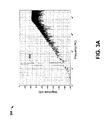
- FIG. 3A illustrates an ideal 217 point fast Fourier transform (FFT) simulation plot 200 (e.g., magnitude vs. frequency) showing a curve 202 of the modulator first quantized out output Y(n) 210 for an 18 kHz ( ⁇ 3 dB) input signal X(t) at the maximum signal amplitude at which the system 100 remains stable.
- FFT 217 point fast Fourier transform
- 3B separately illustrates the three quantization noise sources 212 (first A/D converter 104 ), 214 (second A/D converter 112 c ), and 216 (third quantizer 128 ) modeled for the ideal system 100 .
- the quantization noises associated with the three quantizers are all shaped at second order (e.g., as shown in equations 7 and 8 above). Thus, no one individual quantization noise dominates the others, due to the digital error feedback arrangement in the system 100 .
- Noise Level 1 was simulated having a low frequency gain of 70 dB, a saturation voltage of 1.5V, an 80 MHz bandwidth, and a slew rate of 75 V/usec, wherein third harmonic distortion was simulated at ⁇ 70 dB below input level.
- FIG. 4 shows the power spectrum plot 220 (magnitude vs. frequency) of the signal in the band of interest for GSM applications.
- a solid curve 222 is illustrated corresponding to the ideal simulation of FIG. 3A , which has the lowest noise floor.
- the other curves 224 , 226 , and 228 were obtained by simulation using Noise Level 1 , Noise Level 2 , and the above mentioned non-ideal amplifier 139 , respectively, wherein the noise floor remains at around ⁇ 100 dB in all cases with a very weak second harmonic distortion.
- FIG. 5 shows a signal-to-noise plus distortion ratio (SNDR) vs. input amplitude plot 230 for six different simulations, in which the low frequency gain of the amplifier 139 , as well as the noise levels associated with various noise sources in the system, were varied for a signal band of 100 kHz and an oversampling ratio (OSR) of 96.
- the solid curve 232 illustrates the ideal simulation of an ideal second order modulator with 5 levels of quantization in its feedback, where the noise transfer function is implemented entirely in the analog domain with ideal amplifiers and no noise.
- the dashed curve 234 corresponds to the ideal simulation of the system 100 (e.g., FIG. 3A above).
- curves 236 – 242 are simulation results for the system 100 with different combinations of the amplifier low frequency gain and the noise levels of Table 1.
- Curves 236 and 238 correspond to an integrator amplifier 139 with a low frequency gain of 70 dB simulated using Noise Level 1 and Noise Level 2 , respectively.
- Curves 240 and 242 correspond to a low frequency amplifier gain of 60 dB simulated using Noise Level 1 and Noise Level 2 , respectively.
- FIG. 6 illustrates a comparative plot 250 showing SNDR vs. sampling frequency curves 252 and 254 for the system 100 , in which bandwidths of 100 kHz and 200 kHz are provided, respectively.
- Noise Level 1 and Noise Level 2 e.g., comparing curves 236 and 238 (70 dB amplifier 139 ) or comparing curves 240 and 242 (60 dB amplifier 139 )
- Noise Level 1 and Noise Level 2 e.g., comparing curves 236 and 238 (70 dB amplifier 139 ) or comparing curves 240 and 242 (60 dB amplifier 139 )
- the system 100 is very tolerant of different sources of non-idealities.
- these results show that the system performance is more dependent on the performance of the amplifier 139 than on the non-idealities and noise levels.
- the amplifier parameters employed in the simulations are typical of the amplifiers designed for high-speed applications in wireless systems, wherein the results are believed to be typical of those obtainable in various implementations of the exemplary system 100 and other systems within the scope of the invention.
Landscapes
- Engineering & Computer Science (AREA)
- Theoretical Computer Science (AREA)
- Compression, Expansion, Code Conversion, And Decoders (AREA)
Abstract
A analog-to-digital converters and second order noise shaping systems are presented for providing a noise shaped analog feedback signal to a A/D converter in an analog-to-digital conversion system. The noise shaping system comprises a first order integrator having a single amplifier, and a digital error feedback system comprising a digital signal processing system, in which the digital error feedback system provides an analog feedback signal to the A/D converter with second order noise shaping with respect to a quantization error associated with the A/D converter.
Description
The present invention relates generally to data conversion systems and more particularly to a single amplifier analog-to-digital converter with second order noise shaping.
Analog-to-digital (A/D) converters are electrical circuit devices that convert continuous signals, such as voltages or currents, from the analog domain to the digital domain where the signals are represented by numbers. A variety of A/D converter types exist, including flash A/Ds, sub-ranging A/Ds, successive approximation A/Ds, and integrating A/Ds. Another type is known as a sigma delta or delta sigma (e.g., Δ-Σ) A/D converter that includes a sigma delta modulator operating as a type of noise shaping encoder, typically with a 1–3 bit quantized digital output. Delta sigma (e.g., Δ-Σ) or sigma delta modulators are often used in mixed signal integrated A/D converters, because of their insensitivity to CMOS process linearity and matching problems when compared to other A/D converter types. These features make Δ-Σ based mixed signal solutions very attractive for a number of applications, such as audio, receiver channels of communication devices (wireless in particular), sensor interface circuits and measurement systems.
Delta sigma converters are operated at a significantly higher sampling rate than the bandwidth of the analog input signal, a technique referred to as oversampling, wherein the analog input signal is sampled at a very high sampling rate in order to perform a noise shaping function. The oversampling is commonly performed at a multiple of the Nyquist rate (FN) for a given input signal frequency content (e.g., sampling frequency FS is often 10 to 1000 times FN), wherein quantization noise power is spread over a bandwidth equal to the sampling frequency. Noise shaping filters, typically integrators, are commonly provided in the forward signal path of the delta sigma modulator. Digital filtering is performed on the oversampled digital output to achieve a high resolution, and decimation is employed to reduce the effective sampling rate back to the “Nyquist” rate.
A conventional second order delta sigma modulator 2 is illustrated in FIG. 1 , comprising first and second analog adder/ integrators 4 and 6, respectively. The first adder/integrator 4 comprises a first summing junction 12 and a first integrator (e.g., low pass filter) 16, and the second adder/integrator 6 comprises a second summing junction 18 and an integrator filter 22. The first summing junction 12 receives an analog input signal VIN via an input gain stage 14 i and a first feedback signal FB1 via a feedback gain stage 14 f from a first digital-to-analog converter (DAC or D/A) 112 d. The modulator 2 may be a continuous time modulator or the input signal VIN may be periodically sampled via a switching element 8. An error signal (e.g., the difference between the input and feedback signals according to the relative gains 14 i and 14 f) is provided to the input of the first integrator 16, which provides an integrator output through a second input gain stage 20 i to the second summing junction 18. The summing junction 18 also receives a second feedback signal FB2 via a second feedback gain stage 20 f from a second DAC 26 b. The second summing junction 18 provides an error signal (e.g., the difference between the integrator output signal from the first integrator 16 and the second feedback signal FB2) to the input of the second integrator filter 22.
The modulator 2 further comprises an analog-to-digital (A/D) converter or quantizer 24 receiving the output signal from the second integrator 22. The A/D converter 24 generates an n-bit quantized or digital output signal D1 . . . . Dn, where n is a positive integer. The DAC converters 26 a and 26 b provide the analog feedback signals FB1 and FB2, respectively, in accordance with the digital output D1 . . . Dn of the A/D converter 24. A digital decimation filter 28 reduces undesirable noise in the quantized digital output signal D1 . . . . Dn. The digital filter 28 acts as an anti-aliasing filter with respect to the final sampling rate and filters out higher frequency noise produced by the noise shaping process of the modulator 2. Final data reduction is performed by digitally resampling the filtered output at a lower rate using a process called decimation in the filter 28, wherein decimation removes redundant signal information introduced by the oversampling process.
According to one popular design approach, switched capacitor circuits may be used in constructing the delta sigma converter 2, for example, in the adder/ integrators 4 and 6, the A/D 24, and/or the DACs 26, to facilitate integration in CMOS mixed signal fabrication processes. For instance, in the converter 2, the adder/ integrators 4 and 6 are individually fabricated using an integrator amplifier (e.g., operational amplifier) and a switched capacitor circuit. The switched capacitor circuits may provide for relative gain adjustments of input signal levels by using different capacitor values and/or by grouping of series or parallel-coupled capacitors of like value, wherein the gain adjustments are shown in FIG. 1 as gain stages 14, and 20 in the first and second adder/ integrators 4 and 6, respectively. Also, the DAC converters 26 may individually comprise a group of capacitors of ideally identical capacitance values, for instance, wherein the analog feedback signals FB1 and FB2 are provided by selectively coupling certain ones of the capacitors to certain reference voltages according to the quantized signal D1 . . . Dn. Similarly, the A/D converter 24 may be constructed using switched capacitor circuits.
In many modern applications, such as wireless communications products, low power consumption and low voltage operation are important design considerations for analog-to-digital converters. In the conventional converter 2, the amplifiers inside the integrators 16 and 22 are the major source of current consumption. Furthermore, amplifier nonlinearity becomes more problematic as supply voltage levels are decreased. For a flash type A/D quantizer 24, if the number of levels required is relatively small, for example, 3 or 4 bits (e.g., 8 to 10 levels), the number of comparators and the corresponding power consumption can be reduced. Also, the non-linearity of the DAC converters 26 can be mitigated through dynamic element matching (DEM) techniques. Hence, the effect of DAC imperfections on the quantization noise shaping can be reduced for low voltage operation. However, the ability to significantly reduce power consumption without degrading device performance is limited. While eliminating one stage of the converter 2 may result in lower power consumption, the noise shaping performance would go from second order to first order, whereby the device performance would be worsened. Accordingly, it is desirable to reduce the power consumption of analog-to-digital converter systems, while providing adequate noise shaping.
The following presents a simplified summary in order to provide a basic understanding of one or more aspects of the invention. This summary is not an extensive overview of the invention, and is neither intended to identify key or critical elements of the invention, nor to delineate the scope thereof. Rather, the primary purpose of the summary is to present some concepts of the invention in a simplified form as a prelude to the more detailed description that is presented later. The invention relates analog-to-digital converters and Nth order noise shaping systems therefor, which use digital signal processing and less than N integrator amplifiers to provide analog feedback to an A/D converter that is noise shaped to an Nth order with respect to quantization noise associated with the system A/D converters.
In accordance with an aspect of the invention, an analog-to-digital conversion system is provided, comprising a first A/D converter and a noise shaping system. The first A/D converter provides a first quantized digital output according to a system analog input and according to a noise shaped first analog feedback signal. The noise shaping system provides the first analog feedback signal according to the first digital output. The first feedback signal is noise shaped to an order N with respect to a quantization error associated with the first A/D converter, wherein the noise shaping system has less than an integer number N integrator amplifiers, wherein N is an integer greater than 1. The invention thus provides Nth order noise shaping without the power consumption associated with N integrator amplifiers.
In one example, the noise shaping system comprises a first digital-to-analog converter (DAC), a delta sigma modulator, and a digital error feedback system, and the first DAC provides a first DAC output according to the first digital output. The delta sigma modulator provides a second digital output according to a quantization error for the first DAC (e.g., the difference between the first DAC output and the system analog input). The digital error feedback system provides the first analog feedback signal according to the second digital output, wherein the first analog feedback signal is noise shaped to order N with respect to a quantization error of the delta sigma modulator. In this example, the delta sigma modulator comprises an integrator, a second A/D converter, and a second DAC, where the integrator has less than N integrator amplifiers. The integrator provides an analog integrator output according to the first DAC output, the system analog input, the first analog feedback signal, and an analog modulator feedback signal.
The second A/D converter provides a second digital output according to the integrator output, and the second DAC provides the modulator feedback signal to the integrator according to the second digital output. In this manner, the integrator output is noise shaped by the integrator to an order N−1 with respect to a quantization error associated with the second A/D converter. The noise shaping system in this example further comprises an analog delay system coupled with the integrator and with the first A/D converter, where the analog delay system provides a delayed integrator output signal to the integrator and to the first A/D converter, such that the quantization noise of the second A/D converter is noise shaped to an order N.
The digital error feedback system may comprise a digital signal processing system coupled with the delta sigma modulator. The digital signal processing system provides a third quantized digital output according to the second digital output, wherein the third digital output is noise shaped by the digital signal processing system to order N with respect to a quantization error associated with the delta sigma modulator. The digital error feedback system further comprises a third DAC coupled with the digital signal processing system, where the third DAC provides the first analog feedback signal to the first A/D converter according to the third digital output.
In accordance with another aspect of the invention, a noise shaping system is provided to generate a noise shaped first analog feedback signal in an analog-to-digital conversion system. The noise shaping system comprises a first DAC coupled with the first A/D converter, wherein the first DAC provides a first DAC output according to a first digital output. The system further comprises a delta sigma modulator that provides a second digital output according to a difference between the first DAC output and a system analog input, and a digital error feedback system providing the first analog feedback signal to the first A/D converter according to the second digital output.
The following description and annexed drawings set forth in detail certain illustrative aspects and implementations of the invention. These are indicative of only a few of many ways in which the principles of the invention may be employed.
One or more implementations of the present invention will now be described with reference to the attached drawings, wherein like reference numerals are used to refer to like elements throughout. The invention relates to second or higher order noise shaping in analog-to-digital (A/D) conversion systems, wherein noise shaping or filtering of an Nth order is provided using less than N integrator amplifiers.
The various aspects of the invention are hereinafter illustrated in the context of an exemplary second order A/D conversion system 100 with a single integrator amplifier, wherein second order noise shaping is provided with respect to quantizers (e.g., A/D converters) in the system, using digital signal processing in a digital error feedback system. In this example, a delta sigma modulator is employed to create a digital error signal representing the quantization error of a first A/D converter. However, the invention is not limited to the illustrated examples, wherein A/D conversion systems and noise shaping systems therefor are contemplated, having noise shaping of any order N, where N is an integer greater than 1. Furthermore, while the A/D converters, DACs and other circuits are illustrated below in the context of multi-bit or multi-level digital data, single-bit implementations are also contemplated as falling within the scope of the invention.
As illustrated in FIG. 2A , the system 100 receives the input signal X(t) and feedback signals at a first summer or summation node 102 in a forward signal path that also includes a first A/D converter or quantizer 104. The A/D converter 104 converts the analog signal from the summer 102 into a single or multi-bit first digital output Y(n) at a sampling rate FS that is significantly higher than the Nyquist rate for the bandwidth of the input signal X(t) (e.g., oversampling), and the digital output Y(n) is then provided to a digital filter and decimation system 106 and to a first DAC 108. The exemplary first A/D converter 104 is a flash ADC providing a 5-level (e.g., 3 bit) thermometer coded first digital output Y(n) representative of the system analog input X(t), although any digital-to-analog converter or quantizer type may be employed within the scope of the invention. The system 106 reduces undesirable noise in the digital signal Y(n) and performs decimation by resampling the signal Y(n) at a lower rate to remove redundant signal information introduced by the oversampling process to provide the multi-bit system digital output DOUT representative of the system analog input. The digital decimation system 106 may be constructed using any digital logic and/or analog circuitry within the scope of the invention.
The system 100 further comprises a noise shaping system 110 that provides second order noise shaping for a quantization error associated with the first A/D converter 104. The noise shaping system 110 is coupled to the first A/D converter 104 and provides a first analog feedback signal W(t) to the summer 102 according to the first digital output Y(n), wherein the feedback signal W(t) is second order noise shaped by the system 110 with respect to the quantization error of the A/D converter 104. In accordance with the invention, the noise shaping system 110 has only one integrator amplifier, and digital error feedback is employed in noise shaping the quantization errors.
The noise shaping system 110 comprises the first DAC 108 that provides an analog first DAC output according to the first digital output Y(n), as well as a delta sigma modulator 112 coupled with the first DAC 108 and a digital error feedback system 114. The delta sigma modulator 112 is a first order modulator that quantizes the quantization noise created by the first A/D converter 104, in the form of a second digital output U(k), which can then be operated on with a digital domain noise-shaping transfer function H(z) in the digital error feedback system 114. This approach provides second order noise shaping without requiring two integrator amplifiers, as was the case in conventional second order delta sigma converters (e.g., FIG. 1 above).
The exemplary first order delta sigma modulator 112 comprises an adder/integrator including a summing junction or node 112 a and a first order integrator 112 b coupled with the first DAC 108, wherein the integrator 112 b has only a single integrator amplifier. The modulator 112 further comprises a second A/D converter 112 c quantizing the output of the integrator, and a second DAC 112 d converting the second digital output U(k) to analog form as an internal feedback signal. The adder/ integrator 112 a, 112 b, as well as the second A/D converter 112 c and the second DAC 112 d are implemented as switched capacitor circuits in the exemplary system 100, although these may alternatively be constructed using any suitable circuits or subsystems within the scope of the present invention.
The integrator 112 b provides an analog integrator output according to the first DAC output, according to the system analog input X(t), according to the first analog feedback signal W(t), and according to an analog modulator feedback signal from the second DAC 112 d. The second A/D converter 112 c is coupled with the integrator 112 b and provides the second digital output U(k) according to the integrator output. Within the first order delta sigma modulator 112, the integrator output signal is first order noise shaped by the integrator 112 b with respect to the quantization error of the second A/D converter 112 c. In order to further noise shape the quantization error of the second A/D converter 112 c, the noise shaping system 110 further comprises the error feedback system 114 and an analog delay system or circuit 116, such as a switched capacitor circuit or other system that provides a delayed integrator output feedback signal to the first A/D converter 104 via the summing node 102.
The digital error feedback system 114 is coupled with the delta sigma modulator 112 to receive the second digital output U(k), and is also coupled with the summing node 102 to provide the first analog feedback signal W(t) according to the second digital output U(k). The feedback signal W(t) is digitally noise shaped by the system 114 to the second order with respect to the quantization error of the delta sigma modulator 112, including the quantization error of the second A/D converter 112 c thereof. The exemplary digital error feedback system 114 comprises a digital signal processing (DSP) system 114 a coupled with the delta sigma modulator 112 and a third DAC 114 b coupled with the first A/D converter 104 through the summer 102. This advantageously provides Nth order noise shaping in the system 100 without the addition of integrator amplifiers, whereby low power operation is facilitated.
The DSP system 114 a can be implemented using any suitable digital and sequential logic or other components within the scope of the invention, that provide a third digital output to the DAC 114 b according to the second digital output, which is second order noise shaped with respect to the quantization error of the modulator 112. The third DAC 114 b, in turn, provides the first analog feedback signal W(t) according to the third digital output from the DSP system 114 a.
In the exemplary system 100 of FIG. 2A , the DSP 114 a provides digital first order filtering or noise shaping of the second digital output U(k) via a transfer function H(z) 120 in parallel with a digital domain delay operator (1−z−1) 122, where the outputs of the functions 120 and 122 are provided to a summer 124 along with an internal feedback output from a feedback function z−1H(z) 126. As discussed further below with respect to the simulation results in FIGS. 3A–6 , the noise shaping transfer function H(z) is implemented as a second order low pass filter in the exemplary system 100, although any Nth order noise shaping transfer function may be implemented within the scope of the invention.
The output of the summer 124 is quantized by a third quantizer 128, in this case, a digital-to-digital quantizer that is implemented in the DSP 114 a, the output of which is provided to a summer 130 that subtracts the digital-to-digital quantizer input and provides an error input to the z−1H(z) feedback function 126. Although schematically illustrated as various functional blocks in FIG. 2A , the illustrated functions in the DSP system 114 a may be implemented by any suitable sequential and or combinational logic within the scope of the invention.
Although the exemplary analog-to-digital conversion system 100 is a second order design, the invention is applicable to A/D systems of any order N, wherein the modulator 112 has N−1 or fewer integrator amplifiers, and where N is a positive integer greater than 1. In general, multiple order A/D conversion systems in accordance with the invention may comprise a plurality of integrators in the modulator 112 serially coupled between the modulator input signals from the summer 112 a and the second A/D converter 112 c, as well as a plurality of DAC converters 112 d, with individual DACs 112 d being coupled with the A/D converter 112 c and a corresponding one of the plurality of integrators. Alternatively, a single DAC converter 112 d may provide multiple feedback signals in a multiple order sigma delta modulator 112.
In the exemplary system 100, all the DACs and A/D converters are 5 level thermometer coded devices (e.g., 3 bits), although single bit (e.g., two-level) or other configurations are possible within the scope of the invention. The sigma delta modulator 112 operates to oversample the analog output of the summer 112 a (e.g., oversampling the quantization error of the first A/D converter 104), wherein the digital signal U(k) is an oversampled 5 level thermometer coded second digital output, effectively having 16 to 32 bits in one implementation. If the oversampled output U(k) were itself provided to the third DAC 114 b, the DAC 114 b would need to be large and complex, having a significant number of switching components. In the exemplary system 100, however, the third quantizer 128 and the function z−1H(z) 126 operate to sigma delta modulate the output of the noise shaping function H(z) 120, wherein the output of the third quantizer 128 is also a 5 level thermometer coded signal, making the design of the DAC 114 b relatively small. Thus, the noise shaping functions are provided by the integrator 112 b having a single integrator amplifier, and also through digital processing in the error feedback system 114, by which Nth order noise shaping is accomplished using fewer than N integrator amplifiers.
Referring also to FIGS. 2C–2E , the DACs 108, 112 d, and 114 b, the A/ D converters 104 and 112 c, the summers 102 and 112 a, the delay circuit 116, and the integrator 112 b are implemented using switched capacitor circuits in the exemplary system 100, although these may alternatively be implemented using other components and circuit types within the scope of the invention. Furthermore, one or more of the switched capacitor circuits can be implemented using dynamic element matching (DEM) systems to vary the selection of capacitors, in order to improve system linearity. In this way, the adverse effects of component value deviations (e.g., capacitance mismatch) can be mitigated.
Alternatively, the signals TC1–TC4 can be provided to a thermometer code converter 113 b, which generates binary digital output signals D1, D2, and D3 that may be provided to a binary DAC. In another possible implementation, the thermometer coded signals TC1–TC4 (e.g., or the binary signals D1–D3) may be provided to a dynamic element matching (DEM) system 130, which varies or randomizes the signals according to a DEM algorithm, such as individual level averaging (ILA), group level averaging (GLA), etc., to generate the DAC component select signals S1–S4. Further, the conversion of the thermometer code to the digital output may alternatively be performed in the DEM system 130.
Although illustrated and described in the context of switched capacitor circuits and flash A/D configurations, any A/D converter may be used within the scope of the invention, including non-flash A/Ds and converters that do not employ switched capacitor circuits. In addition, one, some or all of the DACs, A/D converters, and or the adder/integrator, if implemented with switched capacitors, may include DEM circuits or systems within the scope of the invention. Moreover, while the exemplary A/D converters and DACs in the conversion system 100 are multi-level (e.g., multi-bit), single bit devices may alternatively be employed, wherein all such variant implementations are contemplated as falling within the scope of the invention.
In the exemplary DAC 112 d, the analog feedback signal is generated through selective charging of the capacitors C1–C4 according to the switching selection signals S1–S4, wherein the switches SW1–SW4 selectively couple the capacitors C1–C4 with one of the supply voltages −VREF or +VREF so as to provide the analog feedback signal generally corresponding to the second digital output U(k). The charge on the capacitors is then summed at the summing junction 112 a with the charge corresponding to the sampled output from the adder 102 (FIGS. 2A and 2B ) and that from the output of the first DAC 108, wherein relative input and feedback gains may be established according to the relative values of an input capacitance CIN and the DAC capacitances C1–C4. The resulting charge is an error signal and is then provided to the integrator filter 112 b.
Similar switched capacitor circuitry may be incorporated into a single circuit to implement the first DAC 108, wherein the capacitors thereof are selected according to the first digital output Y(n), which may likewise be thermometer coded. The exemplary integrator 112 b is implemented as a switched capacitor circuit with a single integrator amplifier 139 (e.g., operational amplifier) having one or more feedback capacitors Cf and a sampling capacitor Cs and switching components operated according to signals φ3 and φ4 that are also derived from the sampling frequency Fs of the modulator 112. Moreover, in the exemplary system 100, the third DAC 114 b and the first adder (e.g., summing junction) 102 are implemented at the input of the first A/D converter 104 and the first and second DACs 108 and 112 d, respectively, are implemented together with the adder 112 a at the input of the integrator 112 b.
Referring now to FIGS. 2A and 2B , in accordance with the invention, a digital domain error feedback noise shaping is introduced in the DSP 114 a to shape the output of H(z) and also to reduce the number of possible digital signal levels from the oversampled modulator 112, wherein the functions H(z) 120, (1−z−1) 122, z−1H(z) 126, and the third quantizer 128 are implemented completely in the digital domain. It is noted with respect to the integrator 112 b and the analog delay system 116, that while these are shown in FIG. 2A as having z-domain (e.g., digital domain) transfer functions, that these are implemented in analog (e.g., switched capacitor) circuits in the exemplary analog-to-digital conversion system 100.
In order to determine the noise transfer functions (NTF) of the system 100, linear representation are used for the quantizers 104, 112 c, and 128, which are modeled as additive noises with unity gain. The ideal transfer function for the delayed switched capacitor integrator 112 b is:
As shown inFIG. 2A , the second digital output U(k) from the second A/D converter 112 c (e.g., U(z)) can be written in terms of E1, the quantization noise of the first A/D converter 104, as:
U(z)=z −1 E 1(z)+(1−z −1)E 2(z), (2)
where E2 is the quantization noise related to Q2. Similarly, the output of thethird quantizer 128 can be represented as a function of U(z) as:
W(z)=U(z)H(z)−(1−z −1)U(z)+(1−z −1 H(z))E 3(z), (3)
where E3 is the quantization noise associated with thethird quantizer 128. In addition, the first digital output Y(N) of the first A/D converter 104 (e.g., Y(z)) is represented as:
Y(z)=X(z)−W(z)+(1−z −1)E 1(z)+z −1 U(z). (4)
By substituting these equations, the first digital output Y(z) can be rewritten in terms of the quantization noises and the digital transfer function, H(z), as:
Y(z)=X(z)+(1−z −1 H(z))E 1(z)++(1−z −1)(1−H(z))E 2(z)+(1−z −1 H(z))E 3(z), (5)
thereby indicating that all of the noise transfer functions are tuned by the digital transfer function. In one example, H(z) can be implemented in theDSP system 114 a as:
in which case the noise-transfer-functions are determined as:
where NTF1, NTF2, and NTF3 are the noise transfer functions for the quantization noises E1, E2, and E3, respectively. Thus, thesystem 100 provides a second order noise shaping system, wherein all of the noise transfer functions have two DC zeros and two imaginary poles located at Fs/8 and inside the unit circle. In this regard, the system 100 provides second order quantization error noise shaping using a single integrator amplifier 139 (FIG. 2E ).
As shown in
U(z)=z −1 E 1(z)+(1−z −1)E 2(z), (2)
where E2 is the quantization noise related to Q2. Similarly, the output of the
W(z)=U(z)H(z)−(1−z −1)U(z)+(1−z −1 H(z))E 3(z), (3)
where E3 is the quantization noise associated with the
Y(z)=X(z)−W(z)+(1−z −1)E 1(z)+z −1 U(z). (4)
By substituting these equations, the first digital output Y(z) can be rewritten in terms of the quantization noises and the digital transfer function, H(z), as:
Y(z)=X(z)+(1−z −1 H(z))E 1(z)++(1−z −1)(1−H(z))E 2(z)+(1−z −1 H(z))E 3(z), (5)
thereby indicating that all of the noise transfer functions are tuned by the digital transfer function. In one example, H(z) can be implemented in the
in which case the noise-transfer-functions are determined as:
where NTF1, NTF2, and NTF3 are the noise transfer functions for the quantization noises E1, E2, and E3, respectively. Thus, the
Thermal switch noise was also incorporated in the non-ideal circuit simulations, which is generated by random fluctuation of carriers due to thermal energy, having a white spectrum and wide band, and which is controlled by the characteristics of the sampling capacitor (e.g., CIN and Cs in FIG. 2E ). Since it is an accumulative noise, each sampling branch at the input of the real integrator 112 b was modeled with contributing kT/C noise elements contributing to the total noise power depending on a coefficient factor at the branch. Also modeled were mismatches at the quantization levels, harmonic distortion at the amplifier 139, and gain errors. For instance, mismatches in the capacitor values in a CMOS process result in inaccurate quantization levels. Fortunately, all the gains and quantization levels of the flash A/D converters of the system 100 are based on the ratio of capacitors and not on the absolute value. Therefore, a typical mismatch is usually in a range of about 1 or 2%. Due to nonlinearity, a typical switched capacitor amplifier generates harmonic distortion, wherein a differential implementation eliminates the even order harmonics. In this case, therefore, the third harmonic was expected to be the most dominant distortion component.
Simulations were also performed which incorporated the non-ideal behaviors of the circuits in the system 100. In these non-ideal simulations, two different sets of values were used for these non-ideal effects, illustrated as Noise Level 1 and Noise Level 2 in the following Table 1. The amplifier 139 was simulated having a low frequency gain of 70 dB, a saturation voltage of 1.5V, an 80 MHz bandwidth, and a slew rate of 75 V/usec, wherein third harmonic distortion was simulated at −70 dB below input level.
| TABLE 1 | |||
| |
|
||
| Gain Error | 0.25% | 1% | ||
| Quantization Level | 0.5% | 2% | ||
| Mismatch | ||||
| Sampling Cap Size for | 5 |
2 pF | ||
| kT/C Noise | ||||
| Op- |
50 |
100 uV | ||
As shown in FIG. 5 , for a given set of amplifier parameters, particularly at large input signal amplitudes, approximately 4 dB of SNDR is sacrificed between Noise Level 1 and Noise Level 2 (e.g., comparing curves 236 and 238 (70 dB amplifier 139) or comparing curves 240 and 242 (60 dB amplifier 139)). It is noted however, that for a given noise level (e.g., comparing curves 236 and 240 (Noise Level 1) or comparing curves 238 and 242 (Noise Level 2)), approximately 13 dB is lost between the cases where the amplifier low frequency gain is varied from 70 dB to 60 dB. Thus, the simulations of FIG. 5 show that the system 100 is very tolerant of different sources of non-idealities. In addition, these results show that the system performance is more dependent on the performance of the amplifier 139 than on the non-idealities and noise levels. In this regard, the amplifier parameters employed in the simulations are typical of the amplifiers designed for high-speed applications in wireless systems, wherein the results are believed to be typical of those obtainable in various implementations of the exemplary system 100 and other systems within the scope of the invention.
Although the invention has been illustrated and described with respect to one or more implementations, alterations and/or modifications may be made to the illustrated examples without departing from the spirit and scope of the appended claims. In particular regard to the various functions performed by the above described components or structures (assemblies, devices, circuits, systems, etc.), the terms (including a reference to a “means”) used to describe such components are intended to correspond, unless otherwise indicated, to any component or structure which performs the specified function of the described component (e.g., that is functionally equivalent), even though not structurally equivalent to the disclosed structure which performs the function in the herein illustrated exemplary implementations of the invention. In addition, while a particular feature of the invention may have been disclosed with respect to only one of several implementations, such feature may be combined with one or more other features of the other implementations as may be desired and advantageous for any given or particular application. Furthermore, to the extent that the terms “including”, “includes”, “having”, “has”, “with”, or variants thereof are used in either the detailed description and the claims, such terms are intended to be inclusive in a manner similar to the term “comprising”.
Claims (24)
1. An analog-to-digital conversion system, comprising:
a first A/D converter providing a first digital output according to a system analog input and according to a noise shaped first analog feedback signal; and
a noise shaping system with respect to quantization noise associated with said converter of an order N having less than N integrator amplifiers, the noise shaping system being coupled to the first A/D converter and providing the first analog feedback signal according to the first digital output, the first analog feedback signal being noise shaped by the noise shaping system to an order N with respect to a quantization error associated with the first A/D converter, wherein N is an integer greater than 1.
2. The analog-to-digital conversion system of claim 1 , wherein N=2.
3. The analog-to-digital conversion system of claim 2 , wherein the first A/D converter is a flash analog-to-digital converter.
4. The analog-to-digital conversion system of claim 2 , wherein the first A/D converter is a flash ADC providing a thermometer coded first digital output representative of the system analog input.
5. The analog-to-digital conversion system of claim 2 , further comprising a digital decimation filter coupled with the first A/D converter and providing a multi-bit digital output according to the first digital output, the multi-bit digital output being representative of the system analog input.
6. The analog-to-digital conversion system of claim 2 , wherein the noise shaping system comprises:
a first DAC coupled with the first A/D converter, the first DAC providing an analog first DAC output according to the first digital output;
a delta sigma modulator coupled with the first DAC, the delta sigma modulator providing a second digital output according to a difference between the first DAC output and the system analog input; and
a digital error feedback system coupled with the delta sigma modulator, the digital error feedback system providing the first analog feedback signal to the first A/D converter according to the second digital output, the first analog feedback signal being noise shaped by the digital error feedback system to order N with respect to a quantization error associated with the delta sigma modulator.
7. The analog-to-digital conversion system of claim 6 , wherein the delta sigma modulator comprises:
an integrator of order N−1 coupled with the first DAC, the integrator providing an analog integrator output according to the first DAC output, according to the system analog input, according to the first analog feedback signal, and according to an analog modulator feedback signal, the integrator having less than N integrator amplifiers;
a second A/D converter coupled with the integrator, the second A/D converter providing a second digital output according to the integrator output; and
a second DAC coupled with the second A/D converter, the second DAC providing the modulator feedback signal to the integrator according to the second digital output;
wherein the integrator output is noise shaped by the integrator to an order N−1 with respect to a quantization error associated with the second A/D converter.
8. The analog-to-digital conversion system of claim 7 , wherein the noise shaping system further comprises an analog delay system coupled with the integrator and with the first A/D converter, the analog delay system providing an analog delayed integrator output signal to the integrator and to the first A/D converter.
9. The analog-to-digital conversion system of claim 7 , wherein the digital error feedback system comprises:
a digital signal processing system coupled with the delta sigma modulator, the digital signal processing system providing a third digital output according to the second digital output, the third digital output being noise shaped by the digital signal processing system to order N with respect to a quantization error associated with the delta sigma modulator; and
a third DAC coupled with the digital signal processing system, the third DAC providing the first analog feedback signal to the first A/D converter according to the third digital output.
10. The analog-to-digital conversion system of claim 9 , wherein at least one of the first DAC, the second DAC, and the third DAC comprises:
a switched capacitor system comprising a plurality of selectable capacitors providing an analog output corresponding to a digital input code using DAC elements selected according to the digital input code; and
a dynamic element matching system coupled with the switched capacitor system, wherein the dynamic element matching system varies the selection of capacitors.
11. The analog-to-digital conversion system of claim 6 , wherein the digital error feedback system comprises:
a digital signal processing system coupled with the delta sigma modulator, the digital signal processing system providing a third digital output according to the second digital output, the third digital output being noise shaped by the digital signal processing system to order N with respect to a quantization error associated with the delta sigma modulator; and
a third DAC coupled with the digital signal processing system, the third DAC providing the first analog feedback signal to the first A/D converter according to the third digital output.
12. The analog-to-digital conversion system of claim 1 , wherein the noise shaping system comprises:
a first DAC coupled with the first A/D converter, the first DAC providing an analog first DAC output according to the first digital output;
a delta sigma modulator coupled with the first DAC, the delta sigma modulator providing a second digital output according to a difference between the first DAC output and the system analog input; and
a digital error feedback system coupled with the delta sigma modulator, the digital error feedback system providing the first analog feedback signal to the first A/D converter according to the second digital output, the first analog feedback signal being noise shaped by the digital error feedback system to order N with respect to a quantization error associated with the delta sigma modulator.
13. The analog-to-digital conversion system of claim 12 , wherein the delta sigma modulator comprises:
an integrator of order N−1 coupled with the first DAC, the integrator providing an analog integrator output according to the first DAC output, according to the system analog input, according to the first analog feedback signal, and according to an analog modulator feedback signal, the integrator having less than N integrator amplifiers;
a second A/D converter coupled with the integrator, the second A/D converter providing a second digital output according to the integrator output; and
a second DAC coupled with the second A/D converter, the second DAC providing the modulator feedback signal to the integrator according to the second digital output;
wherein the integrator output is noise shaped by the integrator to an order N−1 with respect to a quantization error associated with the second A/D converter.
14. The analog-to-digital conversion system of claim 13 , wherein the noise shaping system further comprises an analog delay system coupled with the integrator and with the first A/D converter, the analog delay system providing an analog delayed integrator output signal to the integrator and to the first A/D converter.
15. The analog-to-digital conversion system of claim 13 , wherein the digital error feedback system comprises:
a digital signal processing system coupled with the delta sigma modulator, the digital signal processing system providing a third digital output according to the second digital output, the third digital output being noise shaped by the digital signal processing system to order N with respect to a quantization error associated with the delta sigma modulator; and
a third DAC coupled with the digital signal processing system, the third DAC providing the first analog feedback signal to the first A/D converter according to the third digital output.
16. The analog-to-digital conversion system of claim 15 , wherein at least one of the first DAC, the second DAC, and the third DAC comprises:
a switched capacitor system comprising a plurality of selectable capacitors providing an analog output corresponding to a digital input code using DAC elements selected according to the digital input code; and
a dynamic element matching system coupled with the switched capacitor system, wherein the dynamic element matching system varies the selection of capacitors.
17. The analog-to-digital conversion system of claim 12 , wherein the digital error feedback system comprises:
a digital signal processing system coupled with the delta sigma modulator, the digital signal processing system providing a third digital output according to the second digital output, the third digital output being noise shaped by the digital signal processing system to order N with respect to a quantization error associated with the delta sigma modulator; and
a third DAC coupled with the digital signal processing system, the third DAC providing the first analog feedback signal to the first A/D converter according to the third digital output.
18. A noise shaping system for providing a noise shaped first analog feedback signal to a first A/D converter in an analog-to-digital conversion system, the noise shaping system comprising:
a first DAC coupled with the first A/D converter, the first DAC providing an analog first DAC output according to a first digital output;
a delta sigma modulator coupled with the first DAC, the delta sigma modulator providing a second digital output according to a difference between the first DAC output and a system analog input; and
a digital error feedback system coupled with the delta sigma modulator, the digital error feedback system providing the first analog feedback signal to the first A/D converter according to the second digital output.
19. The noise shaping system of claim 18 , wherein the delta sigma modulator comprises less than N integrator amplifiers, and wherein the first analog feedback signal is noise shaped to order N with respect to a quantization error associated with the first A/D converter, wherein N is an integer greater than 1.
20. The noise shaping system of claim 18 , wherein the delta sigma modulator comprises:
an integrator coupled with the first DAC, the integrator providing an analog integrator output according to the first DAC output, according to the system analog input, according to the first analog feedback signal, and according to an analog modulator feedback signal, the integrator having N−1 integrator amplifiers;
a second A/D converter coupled with the integrator, the second A/D converter providing a second digital output according to the integrator output; and
a second DAC coupled with the second A/D converter, the second DAC providing the modulator feedback signal to the integrator according to the second digital output;
wherein the integrator output is noise shaped by the integrator to an order N-1 with respect to a quantization error associated with the second A/D converter.
21. The noise shaping system of claim 20 , wherein the noise shaping system further comprises an analog delay system coupled with the integrator and with the first A/D converter, the analog delay system providing an analog delayed integrator output signal to the integrator and to the first A/D converter.
22. The noise shaping system of claim 20 , wherein the digital error feedback system comprises:
a digital signal processing system coupled with the delta sigma modulator, the digital signal processing system providing a third digital output according to the second digital output, the third digital output being noise shaped by the digital signal processing system to order N with respect to a quantization error associated with the delta sigma modulator; and
a third DAC coupled with the digital signal processing system, the third DAC providing the first analog feedback signal to the first A/D converter according to the third digital output.
23. A noise shaping system of an order N for providing a noise shaped analog feedback signal to a first A/D converter in an analog-to-digital conversion system, the noise shaping system comprising:
a DAC receiving a first digital output from the first A/D converter, the DAC providing an analog DAC output according to the first digital output;
a second A/D converter coupled with the DAC, the second A/D converter comprising less than N integrator amplifiers and providing a second digital output according to a difference between the DAC output and a system analog input, N being an integer greater than 1; and
a digital error feedback system coupled with the second A/D converter, the digital error feedback system providing a noise shaped analog feedback signal to the first A/D converter according to the second digital output, wherein the first analog feedback signal is noise shaped by the digital error feedback system to order N with respect to a quantization error associated with the first A/D converter.
24. A second order noise shaping system for providing a noise shaped analog feedback signal to an A/D converter in an analog-to-digital conversion system, the noise shaping system comprising:
a second order integrator having a single amplifier; and
a digital error feedback system comprising a digital signal processing system, the digital error feedback system providing an analog feedback signal to the A/D converter with second order noise shaping with respect to a quantization error associated with the A/D converter.
Priority Applications (1)
| Application Number | Priority Date | Filing Date | Title |
|---|---|---|---|
| US10/698,830 US6940436B2 (en) | 2003-10-31 | 2003-10-31 | Analog-to-digital conversion system with second order noise shaping and a single amplifier |
Applications Claiming Priority (1)
| Application Number | Priority Date | Filing Date | Title |
|---|---|---|---|
| US10/698,830 US6940436B2 (en) | 2003-10-31 | 2003-10-31 | Analog-to-digital conversion system with second order noise shaping and a single amplifier |
Publications (2)
| Publication Number | Publication Date |
|---|---|
| US20050093726A1 US20050093726A1 (en) | 2005-05-05 |
| US6940436B2 true US6940436B2 (en) | 2005-09-06 |
Family
ID=34550770
Family Applications (1)
| Application Number | Title | Priority Date | Filing Date |
|---|---|---|---|
| US10/698,830 Expired - Lifetime US6940436B2 (en) | 2003-10-31 | 2003-10-31 | Analog-to-digital conversion system with second order noise shaping and a single amplifier |
Country Status (1)
| Country | Link |
|---|---|
| US (1) | US6940436B2 (en) |
Cited By (27)
| Publication number | Priority date | Publication date | Assignee | Title |
|---|---|---|---|---|
| US20060158359A1 (en) * | 2005-01-17 | 2006-07-20 | Magrath Anthony J | Pulse width modulator quantisation circuit |
| US7116254B1 (en) * | 2005-04-26 | 2006-10-03 | Fujitsu Limited | Complex type sigma-delta analog to digital conversion unit and receiver |
| US20070139240A1 (en) * | 2005-12-02 | 2007-06-21 | Gerhard Mitteregger | Continuous-time delta-sigma analog digital converter |
| US20080143567A1 (en) * | 2006-12-19 | 2008-06-19 | Morteza Vadipour | Analog digital converter (adc) having improved stability and signal to noise ratio (snr) |
| US20080165043A1 (en) * | 2007-01-10 | 2008-07-10 | Infineon Technologies Ag | Method and apparatus for A/D conversion |
| US20080309535A1 (en) * | 2005-12-05 | 2008-12-18 | Nxp B.V. | Feedforword Sigma-Delta Ad Converter with an Optimized Built-In Filter Function |
| US20090110217A1 (en) * | 2006-05-21 | 2009-04-30 | Trigence Semiconductor, Inc. | Digital/Analogue conversion apparatus |
| US20090140897A1 (en) * | 2007-11-30 | 2009-06-04 | John Healy | Gain matching method and system for single bit gain ranging analog-to-digital converter |
| US20090195426A1 (en) * | 2008-02-06 | 2009-08-06 | Qualcomm Incorporated | Adaptive high-order digital-to-analog conversion |
| US20090309773A1 (en) * | 2008-06-13 | 2009-12-17 | Mostafa Ronaghi | Semiconductor sensor circuit arrangement |
| US20100060499A1 (en) * | 2006-10-31 | 2010-03-11 | Thales | Control closed-loop device and sigma-delta modulator |
| US7768438B1 (en) | 2006-02-03 | 2010-08-03 | Marvell International Ltd. | Low power analog to digital converter |
| US20100219997A1 (en) * | 2006-01-25 | 2010-09-02 | Nxp B.V. | Continuous-time sigma-delta analog-to-digital converter with capacitor and/or resistance digital self-calibration means for rc spread compensation |
| US20100259431A1 (en) * | 2007-08-10 | 2010-10-14 | Rui Yu | System and method for bandpass sigma-delta modulation |
| US20110160883A1 (en) * | 2009-12-16 | 2011-06-30 | Trigence Semiconductor, Inc. | Acoustic playback system |
| US8648638B2 (en) | 2012-01-06 | 2014-02-11 | Via Telecom Co., Ltd. | Electronic chips with slew-rate control at output signals |
| US8682275B2 (en) | 2000-10-11 | 2014-03-25 | Silicon Laboratories Inc. | Apparatus and methods for reducing interference in radio-frequency apparatus |
| US8704581B2 (en) | 2007-04-23 | 2014-04-22 | Qualcomm Incorporated | Switched capacitor integration and summing circuits |
| US8779957B2 (en) | 2012-08-02 | 2014-07-15 | Qualcomm Incorporated | Low distortion feed-forward delta-sigma modulator |
| US9184765B1 (en) | 2014-09-12 | 2015-11-10 | Qualcomm Incorporated | Power efficient noise-coupled delta-sigma modulator |
| US9226053B2 (en) | 2008-06-16 | 2015-12-29 | Trigence Semiconductor, Inc. | Digital speaker driving apparatus |
| US9300310B2 (en) | 2009-12-09 | 2016-03-29 | Trigence Semiconductor, Inc. | Selection device |
| US9520906B2 (en) * | 2014-06-25 | 2016-12-13 | Qualcomm Incorporated | Switched capacitor transmitter circuits and methods |
| US10116323B2 (en) * | 2016-12-16 | 2018-10-30 | Mediatek Inc. | Analog-to-digital converter |
| US10305507B1 (en) * | 2018-03-20 | 2019-05-28 | Texas Instruments Incorporated | First-order sigma-delta analog-to-digital converter |
| US10404270B2 (en) | 2017-12-06 | 2019-09-03 | Samsung Electronics Co., Ltd. | Semiconductor device and operating method thereof |
| US11509327B2 (en) | 2020-08-10 | 2022-11-22 | Analog Devices, Inc. | System and method to enhance noise performance in a delta sigma converter |
Families Citing this family (27)
| Publication number | Priority date | Publication date | Assignee | Title |
|---|---|---|---|---|
| US7176821B1 (en) * | 2005-10-03 | 2007-02-13 | Texas Instruments Incorported | Reduced area digital sigma-delta modulator |
| DE102006002901B4 (en) * | 2006-01-20 | 2013-03-07 | Infineon Technologies Ag | Multi-bit sigma-delta converter |
| US7822160B1 (en) | 2006-02-03 | 2010-10-26 | Marvell International Ltd. | Digitally-assisted power reduction technique for IQ pipeline ADCs used in wireless receivers |
| US8045605B2 (en) * | 2006-12-25 | 2011-10-25 | Advantest Corporation | Jitter amplifier circuit, signal generation circuit, semiconductor chip, and test apparatus |
| ATE534193T1 (en) * | 2008-07-01 | 2011-12-15 | Ericsson Telefon Ab L M | DELTA-SIGMA ANALOG TO DIGITAL CONVERTER, RADIO RECEIVER, COMMUNICATION DEVICE, METHOD AND COMPUTER PROGRAM |
| US8427350B2 (en) * | 2008-10-23 | 2013-04-23 | Nxp B.V. | Sigma-delta modulator |
| KR101531877B1 (en) * | 2009-01-13 | 2015-06-26 | 삼성전자주식회사 | Switched-capacitor integrator for eliminating floating node reset operation and devices having the same |
| US8346091B2 (en) * | 2009-04-29 | 2013-01-01 | Andrew Llc | Distributed antenna system for wireless network systems |
| US9680498B2 (en) | 2009-06-26 | 2017-06-13 | Syntropy Systems, Llc | Sampling/quantization converters |
| US9209829B2 (en) * | 2009-06-26 | 2015-12-08 | Syntropy Systems, Llc | Sampling/quantization converters |
| TWI448071B (en) * | 2011-02-22 | 2014-08-01 | Ind Tech Res Inst | System with variably combined common-mode and differential-mode digital output |
| US9197240B1 (en) * | 2014-07-10 | 2015-11-24 | Taiwan Semiconductor Manufacturing Company, Ltd. | Method and circuit for noise shaping SAR analog-to-digital converter |
| US10020818B1 (en) | 2016-03-25 | 2018-07-10 | MY Tech, LLC | Systems and methods for fast delta sigma modulation using parallel path feedback loops |
| US10530372B1 (en) | 2016-03-25 | 2020-01-07 | MY Tech, LLC | Systems and methods for digital synthesis of output signals using resonators |
| US10340932B2 (en) * | 2016-04-29 | 2019-07-02 | Analog Devices, Inc. | Techniques for power efficient oversampling successive approximation register |
| WO2018094380A1 (en) | 2016-11-21 | 2018-05-24 | MY Tech, LLC | High efficiency power amplifier architectures for rf applications |
| US10566994B2 (en) | 2016-12-19 | 2020-02-18 | Cable Television Laboratories, Inc. | System and methods for virtualizing delta sigma digitization |
| US10805058B2 (en) | 2016-12-19 | 2020-10-13 | Cable Television Laboratories, Inc. | Systems and methods for mapping and demapping digitized signals for optical transmission |
| US10763963B2 (en) * | 2016-12-19 | 2020-09-01 | Cable Television Laboratories, Inc | System and methods for efficient digitization in hybrid fiber-coaxial networks |
| US10312926B2 (en) * | 2017-10-30 | 2019-06-04 | Analog Devices Global Unlimited Company | Noise-shaping analog-to-digital converter |
| US10644718B1 (en) * | 2019-05-07 | 2020-05-05 | University Of Macau | Single-loop linear-exponential multi-bit incremental analog-to-digital converter |
| FR3105897B1 (en) * | 2019-12-26 | 2023-10-27 | Thales Sa | Analog-to-digital conversion device comprising two cascaded analog-to-digital conversion stages with successive approximation register and noise shaping, and associated electronic sensor |
| US10931299B1 (en) * | 2020-03-31 | 2021-02-23 | Taiwan Semiconductor Manufacturing Company, Ltd. | Analog to digital converter with VCO-based and pipelined quantizers |
| US11933919B2 (en) | 2022-02-24 | 2024-03-19 | Mixed-Signal Devices Inc. | Systems and methods for synthesis of modulated RF signals |
| US11962317B2 (en) * | 2022-05-31 | 2024-04-16 | Qualcomm Incorporated | Noise shaping in multi-stage analog-to-digital converters |
| US20230396264A1 (en) * | 2022-06-01 | 2023-12-07 | Analog Devices International Unlimited Company | High speed sar adc |
| US20240048150A1 (en) * | 2022-08-04 | 2024-02-08 | Nxp B.V. | System and method of reducing delta-sigma modulator error using force-and-correction |
Citations (9)
| Publication number | Priority date | Publication date | Assignee | Title |
|---|---|---|---|---|
| US5065157A (en) | 1990-04-06 | 1991-11-12 | General Electric Company | High order sigma delta oversampled analog-to-digital converter integrated circuit network with minimal power dissipation and chip area requirements |
| US5103229A (en) | 1990-04-23 | 1992-04-07 | General Electric Company | Plural-order sigma-delta analog-to-digital converters using both single-bit and multiple-bit quantization |
| US5181032A (en) | 1991-09-09 | 1993-01-19 | General Electric Company | High-order, plural-bit-quantization sigma-delta modulators using single-bit digital-to-analog conversion feedback |
| US5305004A (en) | 1992-09-29 | 1994-04-19 | Texas Instruments Incorporated | Digital to analog converter for sigma delta modulator |
| US6473019B1 (en) * | 2001-06-21 | 2002-10-29 | Nokia Corporation | Low capacitance, low kickback noise input stage of a multi-level quantizer with dithering and multi-threshold generation for a multi-bit sigma-delta modulator |
| US6611221B1 (en) | 2002-08-26 | 2003-08-26 | Texas Instruments Incorporated | Multi-bit sigma-delta modulator employing dynamic element matching using adaptively randomized data-weighted averaging |
| US6697004B1 (en) * | 2001-10-01 | 2004-02-24 | Silicon Wave, Inc. | Partial mismatch-shaping digital-to-analog converter |
| US6707409B1 (en) * | 2002-09-11 | 2004-03-16 | University Of Rochester | Sigma-delta analog to digital converter architecture based upon modulator design employing mirrored integrator |
| US6710729B1 (en) * | 2002-10-10 | 2004-03-23 | Faraday Technology Corp. | Idle channel tone and periodic noise suppression for sigma-delta modulator using feedback-quantizer |
-
2003
- 2003-10-31 US US10/698,830 patent/US6940436B2/en not_active Expired - Lifetime
Patent Citations (9)
| Publication number | Priority date | Publication date | Assignee | Title |
|---|---|---|---|---|
| US5065157A (en) | 1990-04-06 | 1991-11-12 | General Electric Company | High order sigma delta oversampled analog-to-digital converter integrated circuit network with minimal power dissipation and chip area requirements |
| US5103229A (en) | 1990-04-23 | 1992-04-07 | General Electric Company | Plural-order sigma-delta analog-to-digital converters using both single-bit and multiple-bit quantization |
| US5181032A (en) | 1991-09-09 | 1993-01-19 | General Electric Company | High-order, plural-bit-quantization sigma-delta modulators using single-bit digital-to-analog conversion feedback |
| US5305004A (en) | 1992-09-29 | 1994-04-19 | Texas Instruments Incorporated | Digital to analog converter for sigma delta modulator |
| US6473019B1 (en) * | 2001-06-21 | 2002-10-29 | Nokia Corporation | Low capacitance, low kickback noise input stage of a multi-level quantizer with dithering and multi-threshold generation for a multi-bit sigma-delta modulator |
| US6697004B1 (en) * | 2001-10-01 | 2004-02-24 | Silicon Wave, Inc. | Partial mismatch-shaping digital-to-analog converter |
| US6611221B1 (en) | 2002-08-26 | 2003-08-26 | Texas Instruments Incorporated | Multi-bit sigma-delta modulator employing dynamic element matching using adaptively randomized data-weighted averaging |
| US6707409B1 (en) * | 2002-09-11 | 2004-03-16 | University Of Rochester | Sigma-delta analog to digital converter architecture based upon modulator design employing mirrored integrator |
| US6710729B1 (en) * | 2002-10-10 | 2004-03-23 | Faraday Technology Corp. | Idle channel tone and periodic noise suppression for sigma-delta modulator using feedback-quantizer |
Non-Patent Citations (6)
| Title |
|---|
| "A 1.5V 2.4/2.9mW 79/50dB DR Sigma Delta Modulator for GSM/WCDMA in a 0.13um Digital Process", G. Gomez and B. Haroun, Solid State Circuits Conference, Digest of Technical Papers, vol. 1, pp. 306-307, Feb. 2002 San Francisco, CA, and Visuals Supplement, pp. 242, 243, 490. |
| "A Direct Digital Synthesizer with a tunable Error Feedback Structure", Jouko Jankka, IEEE Transactions on Communications, vol. 45, No. 4, Apr., 1997, pp. 416-420. |
| "A Noise-Shaping Coder Topology for 15+ Bit Converters", L. Richard Carley, IEEE Journal of Solid-State Circuits, vol. 24, No. 2, Apr., 1989, pp. 267-273. |
| "Behavioral Modeling of Seitched-Capacitor Sigma-Delta Modulators", Piero Malcovati, Simona Brigati, Fabrizio Francesconi, Franco Maloberti, Paolo Cusianato and Andrea Baschirotto, IEEE Transactions on Circuits and Systems; Fundamental Theory and Applications, vol. 50, No. 3, Mar., 2003, pp. 352-364. |
| "Multibit Epsilon-Delta A/D Converter Incorporating A Novel Class of Dynamic Element Matching Techniques", Bosco H. Leung and Schat Sutarja, IEEE Transactions on Circuits and Systems, Analog and Digital Signal Processing, vol. 39, No. 1, Jan., 1992, pp. 35-51. |
| Institute of Electrical and Electronics Engineers, 2002 Digest of Technical Papers and Visuals Supplement 2002 to the Digest of Technical Papers, IEEE International Solid-State Circuits conference, Vol. Forty-Five, ISSN 0193-6530, 13.3 "A Dual-Mode 80MHz Bandpass DeltaEpsilon Modulator for a GSM/WCDMA IF-Receiver" T. Salo, T. Hollman, S. Lingfors and K. Halonen, 7 pgs. |
Cited By (47)
| Publication number | Priority date | Publication date | Assignee | Title |
|---|---|---|---|---|
| US8682275B2 (en) | 2000-10-11 | 2014-03-25 | Silicon Laboratories Inc. | Apparatus and methods for reducing interference in radio-frequency apparatus |
| US7205917B2 (en) * | 2005-01-17 | 2007-04-17 | Wolfson Microelectronics Plc | Pulse width modulator quantisation circuit |
| US20060158359A1 (en) * | 2005-01-17 | 2006-07-20 | Magrath Anthony J | Pulse width modulator quantisation circuit |
| US7116254B1 (en) * | 2005-04-26 | 2006-10-03 | Fujitsu Limited | Complex type sigma-delta analog to digital conversion unit and receiver |
| US20060238395A1 (en) * | 2005-04-26 | 2006-10-26 | Fujitsu Limited | Complex type sigma-delta analog to digital conversion unit and receiver |
| US20070139240A1 (en) * | 2005-12-02 | 2007-06-21 | Gerhard Mitteregger | Continuous-time delta-sigma analog digital converter |
| US7405687B2 (en) * | 2005-12-02 | 2008-07-29 | National Semiconductor Germany Ag | Continuous-time delta-sigma analog digital converter |
| US7554474B2 (en) * | 2005-12-05 | 2009-06-30 | Nxp B.V. | Feedforward sigma-delta ad converter with an optimized built-in filter function |
| US20080309535A1 (en) * | 2005-12-05 | 2008-12-18 | Nxp B.V. | Feedforword Sigma-Delta Ad Converter with an Optimized Built-In Filter Function |
| US7944385B2 (en) * | 2006-01-25 | 2011-05-17 | Nxp B.V. | Continuous-time sigma-delta analog-to-digital converter with capacitor and/or resistance digital self-calibration means for RC spread compensation |
| US20100219997A1 (en) * | 2006-01-25 | 2010-09-02 | Nxp B.V. | Continuous-time sigma-delta analog-to-digital converter with capacitor and/or resistance digital self-calibration means for rc spread compensation |
| US7768438B1 (en) | 2006-02-03 | 2010-08-03 | Marvell International Ltd. | Low power analog to digital converter |
| US9276540B2 (en) | 2006-05-21 | 2016-03-01 | Trigence Semiconductors, Inc. | Digital/analogue conversion apparatus |
| US9681231B2 (en) | 2006-05-21 | 2017-06-13 | Trigence Semiconductor, Inc. | Digital/analog conversion apparatus |
| US20090110217A1 (en) * | 2006-05-21 | 2009-04-30 | Trigence Semiconductor, Inc. | Digital/Analogue conversion apparatus |
| US8423165B2 (en) | 2006-05-21 | 2013-04-16 | Trigence Semiconductor, Inc. | Digital/analogue conversion apparatus |
| US7965210B2 (en) * | 2006-10-31 | 2011-06-21 | Thales | Control closed-loop device and sigma-delta modulator |
| US20100060499A1 (en) * | 2006-10-31 | 2010-03-11 | Thales | Control closed-loop device and sigma-delta modulator |
| US7436336B2 (en) * | 2006-12-19 | 2008-10-14 | Broadcom Corporation | Analog digital converter (ADC) having improved stability and signal to noise ratio (SNR) |
| US20080143567A1 (en) * | 2006-12-19 | 2008-06-19 | Morteza Vadipour | Analog digital converter (adc) having improved stability and signal to noise ratio (snr) |
| US20080165043A1 (en) * | 2007-01-10 | 2008-07-10 | Infineon Technologies Ag | Method and apparatus for A/D conversion |
| US7453382B2 (en) * | 2007-01-10 | 2008-11-18 | Infineon Technologies Ag | Method and apparatus for A/D conversion |
| US8704581B2 (en) | 2007-04-23 | 2014-04-22 | Qualcomm Incorporated | Switched capacitor integration and summing circuits |
| US20100259431A1 (en) * | 2007-08-10 | 2010-10-14 | Rui Yu | System and method for bandpass sigma-delta modulation |
| US8072363B2 (en) * | 2007-08-10 | 2011-12-06 | National University Of Singapore | System and method for bandpass sigma-delta modulation |
| US7705757B2 (en) * | 2007-11-30 | 2010-04-27 | Analog Devices, Inc. | Gain matching method and system for single bit gain ranging analog-to-digital converter |
| US20090140897A1 (en) * | 2007-11-30 | 2009-06-04 | John Healy | Gain matching method and system for single bit gain ranging analog-to-digital converter |
| US7825844B2 (en) | 2008-02-06 | 2010-11-02 | Qualcomm Incorporated | Adaptive high-order digital-to-analog conversion |
| US20090195426A1 (en) * | 2008-02-06 | 2009-08-06 | Qualcomm Incorporated | Adaptive high-order digital-to-analog conversion |
| US7782237B2 (en) | 2008-06-13 | 2010-08-24 | The Board Of Trustees Of The Leland Stanford Junior University | Semiconductor sensor circuit arrangement |
| US20090309773A1 (en) * | 2008-06-13 | 2009-12-17 | Mostafa Ronaghi | Semiconductor sensor circuit arrangement |
| US9226053B2 (en) | 2008-06-16 | 2015-12-29 | Trigence Semiconductor, Inc. | Digital speaker driving apparatus |
| US9693136B2 (en) | 2008-06-16 | 2017-06-27 | Trigence Semiconductor Inc. | Digital speaker driving apparatus |
| US9300310B2 (en) | 2009-12-09 | 2016-03-29 | Trigence Semiconductor, Inc. | Selection device |
| US9735796B2 (en) | 2009-12-09 | 2017-08-15 | Trigence Semiconductor, Inc. | Selection device |
| US9219960B2 (en) * | 2009-12-16 | 2015-12-22 | Trigence Semiconductor Inc. | Acoustic playback system |
| US20110160883A1 (en) * | 2009-12-16 | 2011-06-30 | Trigence Semiconductor, Inc. | Acoustic playback system |
| US8648638B2 (en) | 2012-01-06 | 2014-02-11 | Via Telecom Co., Ltd. | Electronic chips with slew-rate control at output signals |
| US8779957B2 (en) | 2012-08-02 | 2014-07-15 | Qualcomm Incorporated | Low distortion feed-forward delta-sigma modulator |
| US9520906B2 (en) * | 2014-06-25 | 2016-12-13 | Qualcomm Incorporated | Switched capacitor transmitter circuits and methods |
| US9531409B2 (en) | 2014-06-25 | 2016-12-27 | Qualcomm Incorporated | Switched capacitor transmitter circuits and methods |
| US9184765B1 (en) | 2014-09-12 | 2015-11-10 | Qualcomm Incorporated | Power efficient noise-coupled delta-sigma modulator |
| US10116323B2 (en) * | 2016-12-16 | 2018-10-30 | Mediatek Inc. | Analog-to-digital converter |
| US10404270B2 (en) | 2017-12-06 | 2019-09-03 | Samsung Electronics Co., Ltd. | Semiconductor device and operating method thereof |
| US10305507B1 (en) * | 2018-03-20 | 2019-05-28 | Texas Instruments Incorporated | First-order sigma-delta analog-to-digital converter |
| US11509327B2 (en) | 2020-08-10 | 2022-11-22 | Analog Devices, Inc. | System and method to enhance noise performance in a delta sigma converter |
| US11658678B2 (en) | 2020-08-10 | 2023-05-23 | Analog Devices, Inc. | System and method to enhance noise performance in a delta sigma converter |
Also Published As
| Publication number | Publication date |
|---|---|
| US20050093726A1 (en) | 2005-05-05 |
Similar Documents
| Publication | Publication Date | Title |
|---|---|---|
| US6940436B2 (en) | Analog-to-digital conversion system with second order noise shaping and a single amplifier | |
| US5982317A (en) | Oversampled digital-to-analog converter based on nonlinear separation and linear recombination | |
| US7576671B2 (en) | Mismatch-shaping dynamic element matching systems and methods for multi-bit sigma-delta data converters | |
| US6304608B1 (en) | Multibit sigma-delta converters employing dynamic element matching with reduced baseband tones | |
| US6426714B1 (en) | Multi-level quantizer with current mode DEM switch matrices and separate DEM decision logic for a multibit sigma delta modulator | |
| US7049990B2 (en) | Single loop feed-forward modulator with summing flash quantizer and multi-bit feedback | |
| EP1147609B1 (en) | Method and apparatus for eliminating clock jitter in continuous-time delta-sigma analog-to-digital converters | |
| US7616141B2 (en) | Digital-to-analog converter | |
| Caldwell et al. | Incremental data converters at low oversampling ratios | |
| Dedic | A sixth-order triple-loop sigma-delta CMOS ADC with 90 dB SNR and 100 kHz bandwidth | |
| Wang et al. | Robust continuous-time MASH delta sigma modulator | |
| Shakya et al. | Efficient calibration of feedback DAC in delta sigma modulators | |
| Aboudina et al. | A New DAC mismatch shaping technique for sigma–delta modulators | |
| Kiss | Adaptive digital compensation of analog circuit imperfections for cascaded delta-sigma analog-to-digital converters | |
| Lindfors et al. | N‐path dynamic element matching for multibit bandpass ΣΔ modulators | |
| Li et al. | Dynamic element matching in low oversampling delta sigma ADCs | |
| Rusu et al. | A multi-bit sigma-delta modulator for wideband applications | |
| Hong et al. | A 36-mW 320-MHz CMOS continuous-time sigma-delta modulator with 10-MHz bandwidth and 12-bit resolution | |
| Mohammadi et al. | On the design of a 2-2-0 MASH delta-sigma-pipeline modulator | |
| US20240063812A1 (en) | Excess Loop Delay Compensation for a Delta-Sigma Modulator | |
| Han et al. | Sturdy-MASH delta-sigma modulator with noise-shaped integrating quantizer and dual-DAC DWA | |
| Colodro et al. | Time-interleaved multirate sigma-delta modulators | |
| Yan | Jitter Tolerant Hybrid Sigma-Delta Modulator | |
| Maghami et al. | Multirate double-sampling hybrid CT/DT sigma-delta modulators for wideband applications | |
| Su et al. | A fourth-order cascaded sigma-delta modulator with DAC error cancellation technique |
Legal Events
| Date | Code | Title | Description |
|---|---|---|---|
| AS | Assignment |
Owner name: TEXAS INSTRUMENTS INCORPORATED, TEXAS Free format text: ASSIGNMENT OF ASSIGNORS INTEREST;ASSIGNORS:HEZAR, RAHMI;ALTUN, OGUZ;REEL/FRAME:014655/0636 Effective date: 20031031 |
|
| STCF | Information on status: patent grant |
Free format text: PATENTED CASE |
|
| FPAY | Fee payment |
Year of fee payment: 4 |
|
| FPAY | Fee payment |
Year of fee payment: 8 |
|
| FPAY | Fee payment |
Year of fee payment: 12 |