US6866552B2 - Electrical connector with a terminal pin alignment plate - Google Patents

Electrical connector with a terminal pin alignment plate Download PDF

Info

Publication number
US6866552B2
US6866552B2 US10/374,964 US37496403A US6866552B2 US 6866552 B2 US6866552 B2 US 6866552B2 US 37496403 A US37496403 A US 37496403A US 6866552 B2 US6866552 B2 US 6866552B2
Authority
US
United States
Prior art keywords
pin
alignment plate
printed circuit
circuit board
housing
Prior art date
Legal status (The legal status is an assumption and is not a legal conclusion. Google has not performed a legal analysis and makes no representation as to the accuracy of the status listed.)
Expired - Lifetime
Application number
US10/374,964
Other versions
US20040166705A1 (en
Inventor
David F. Koehler
Current Assignee (The listed assignees may be inaccurate. Google has not performed a legal analysis and makes no representation or warranty as to the accuracy of the list.)
Molex LLC
Original Assignee
Molex LLC
Priority date (The priority date is an assumption and is not a legal conclusion. Google has not performed a legal analysis and makes no representation as to the accuracy of the date listed.)
Filing date
Publication date
Application filed by Molex LLC filed Critical Molex LLC
Priority to US10/374,964 priority Critical patent/US6866552B2/en
Assigned to MOLEX INCORPORATED reassignment MOLEX INCORPORATED ASSIGNMENT OF ASSIGNORS INTEREST (SEE DOCUMENT FOR DETAILS). Assignors: KOEHLER, DAVID F.
Publication of US20040166705A1 publication Critical patent/US20040166705A1/en
Application granted granted Critical
Publication of US6866552B2 publication Critical patent/US6866552B2/en
Anticipated expiration legal-status Critical
Assigned to MOLEX, LLC reassignment MOLEX, LLC CHANGE OF NAME (SEE DOCUMENT FOR DETAILS). Assignors: MOLEX INCORPORATED
Expired - Lifetime legal-status Critical Current

Links

Images

Classifications

    • HELECTRICITY
    • H01ELECTRIC ELEMENTS
    • H01RELECTRICALLY-CONDUCTIVE CONNECTIONS; STRUCTURAL ASSOCIATIONS OF A PLURALITY OF MUTUALLY-INSULATED ELECTRICAL CONNECTING ELEMENTS; COUPLING DEVICES; CURRENT COLLECTORS
    • H01R12/00Structural associations of a plurality of mutually-insulated electrical connecting elements, specially adapted for printed circuits, e.g. printed circuit boards [PCB], flat or ribbon cables, or like generally planar structures, e.g. terminal strips, terminal blocks; Coupling devices specially adapted for printed circuits, flat or ribbon cables, or like generally planar structures; Terminals specially adapted for contact with, or insertion into, printed circuits, flat or ribbon cables, or like generally planar structures
    • H01R12/70Coupling devices
    • H01R12/7005Guiding, mounting, polarizing or locking means; Extractors
    • HELECTRICITY
    • H01ELECTRIC ELEMENTS
    • H01RELECTRICALLY-CONDUCTIVE CONNECTIONS; STRUCTURAL ASSOCIATIONS OF A PLURALITY OF MUTUALLY-INSULATED ELECTRICAL CONNECTING ELEMENTS; COUPLING DEVICES; CURRENT COLLECTORS
    • H01R12/00Structural associations of a plurality of mutually-insulated electrical connecting elements, specially adapted for printed circuits, e.g. printed circuit boards [PCB], flat or ribbon cables, or like generally planar structures, e.g. terminal strips, terminal blocks; Coupling devices specially adapted for printed circuits, flat or ribbon cables, or like generally planar structures; Terminals specially adapted for contact with, or insertion into, printed circuits, flat or ribbon cables, or like generally planar structures
    • H01R12/70Coupling devices
    • H01R12/71Coupling devices for rigid printing circuits or like structures
    • H01R12/72Coupling devices for rigid printing circuits or like structures coupling with the edge of the rigid printed circuits or like structures
    • H01R12/722Coupling devices for rigid printing circuits or like structures coupling with the edge of the rigid printed circuits or like structures coupling devices mounted on the edge of the printed circuits
    • H01R12/724Coupling devices for rigid printing circuits or like structures coupling with the edge of the rigid printed circuits or like structures coupling devices mounted on the edge of the printed circuits containing contact members forming a right angle
    • HELECTRICITY
    • H05ELECTRIC TECHNIQUES NOT OTHERWISE PROVIDED FOR
    • H05KPRINTED CIRCUITS; CASINGS OR CONSTRUCTIONAL DETAILS OF ELECTRIC APPARATUS; MANUFACTURE OF ASSEMBLAGES OF ELECTRICAL COMPONENTS
    • H05K3/00Apparatus or processes for manufacturing printed circuits
    • H05K3/30Assembling printed circuits with electric components, e.g. with resistor
    • H05K3/306Lead-in-hole components, e.g. affixing or retention before soldering, spacing means

Definitions

  • This invention generally relates to the art of electrical connectors and, particularly, to an electrical connector which has a terminal pin alignment plate which mounts a printed circuit board thereon.
  • an electrical connector typically includes an insulating or dielectric housing which mounts a plurality of conductive terminals having contact portions for engaging the terminals of a complementary mating connector.
  • the terminals also have terminating portions for connection to electrical conductors such as discrete electrical wires or the circuit traces on a printed circuit board.
  • the terminating portions of the terminals comprise pin portions for insertion into holes in a printed circuit board and for electrical connection to the circuit traces on the board and/or in the holes.
  • pin alignment plates have been used, wherein a plate has a plurality of holes for receiving the terminal pin portions to maintain the alignment and spacing of the pin portions and prevent bending thereof or damage thereto.
  • the alignment plates may be removed or remain in place before the connector is mated, or it has been known to provide an arrangement whereby the alignment plate moves from an outer protecting position, inwardly along the pin portions to an inner mating position, such as during insertion of the pin portions into holes in a printed circuit board.
  • the present invention is directed to a unique improvement in such systems wherein the terminal alignment plate is provided with means for mounting a printed circuit board thereto for movement therewith.
  • An object, therefore, of the invention is to provide a new and improved electrical connector with a pin alignment plate that mounts a printed circuit board thereon.
  • the connector includes a dielectric housing having a plurality of conductive terminals mounted thereon with pin portions projecting therefrom.
  • a pin alignment plate has a plurality of apertures for receiving the pin portions of the terminals.
  • the pin alignment plate is movably mounted on the housing for movement from a protecting position generally at distal ends of the pin portions to a pin-exposing position spaced inwardly of the distal ends.
  • the pin alignment plate includes means for mounting a printed circuit board thereon for movement therewith between said positions.
  • first complementary interengaging latch means between the pin alignment plate and the housing for holding the plate in its protecting position.
  • Second complementary interengaging latch means are provided between the pin alignment plate and the housing for holding the plate in its pin-exposing position.
  • the means for mounting the printed circuit board on the pin alignment plate comprises at least one latch arm for projecting through a mounting hole in the printed circuit board.
  • the latch arm is flexible and includes a hook portion for snapping into latching engagement with one side of the printed circuit board as the latch arm is inserted through the mounting hole in the board.
  • the housing includes a relatively rigid backup member for positioning behind the latch arm to prevent the latch arm from flexing out of engagement with the printed circuit board when the pin alignment plate is in its pin-exposing position.
  • the combination of the electrical connector with a printed circuit board is contemplated, with the board having complementary mounting means, such as the mounting hole, for cooperating with the mounting means on the pin alignment plate to facilitate mounting the board on the plate.
  • FIG. 1 is a perspective view of the rear or terminating end of a header connector for receiving the pin alignment plate of the invention
  • FIG. 2 is an enlarged fragmented perspective view of one end of the header connector
  • FIG. 3 is a perspective view of the pin alignment plate
  • FIG. 4 is an enlarged, fragmented perspective view of the left-hand end of the pin alignment plate as viewed in FIG. 3 ;
  • FIG. 5 is an enlarged, fragmented perspective view of the back side of the left-hand end of the pin alignment plate as viewed in FIG. 3 ;
  • FIG. 6 is a perspective view of the header connector, with the pin alignment plate mounted thereto in its outer or protecting position;
  • FIG. 7 is an enlarged, fragmented perspective view of the left-hand end of FIG. 6 ;
  • FIG. 8 is a perspective view of the header connector, with a printed circuit board mounted to the pin alignment plate and with the plate still in its outer or protecting position;
  • FIG. 9 is an enlarged, fragmented and sectional view of the left-hand end of FIG. 8 ;
  • FIG. 10 is an enlarged, fragmented perspective view of one end of the assembly of FIGS. 8 and 9 , with the pin alignment plate and printed circuit board conjointly moved to the pin-exposing position;
  • FIG. 11 is a view similar to that of FIG. 9 , but with the pin alignment plate and printed circuit board having been moved conjointly to the pin-exposing position of FIG. 10 .
  • FIGS. 1 and 2 show an electrical connector in the form of a header connector, generally designated 14 , which mounts a pin alignment plate, generally designated 16 in FIGS. 3-5 , according to the invention. It immediately should be understood that header connector 14 is but one example of an electrical connector with which the pin alignment plate system of the invention is applicable or useful.
  • header connector 14 includes a dielectric housing, generally designated 18 , which may be unitarily molded of plastic material.
  • the housing has a pair of forwardly projecting mating portions 20 for mating with a pair of complementary mating connectors (not shown).
  • the housing defines a rear terminating face 22 from which a pair of end wings 24 and a center wing 26 project rearwardly from terminating face 22 .
  • a cylindrical center mounting post 28 projects upwardly from center wing 26
  • a pair of semi-cylindrical mounting posts 30 project upwardly from end wings 24 .
  • Mounting post 30 form relaively rigid backup members for flexible latch arms on pin alignment plate 16 as will be described in detail hereinafter.
  • a plurality of conductive terminals are mounted in dielectric housing 18 of header connector 14 .
  • the terminals have contact portions (not visible in the drawings) which project into mating portions 20 for engaging the terminals of the complementary mating connectors.
  • the terminals have pin portions 32 a which project from rear terminating face 22 of housing 18 and which are bent at right angles to extend in the same direction as mounting posts 28 and 30 .
  • Pin portions 32 a of the terminals have distal ends 32 b.
  • a first latch boss 34 projects rearwardly from terminating face 22 of housing 18 inside each opposite end wing 24 and at opposite sides of center wing 26 .
  • This first latch boss has an upwardly facing chamfered or angled surface 34 a , as viewed in the drawings.
  • a second latch boss 36 is formed in a groove 38 inside each end wing 24 and on opposite sides of center wing 26 .
  • This second latch boss also has an upwardly facing chamfered or angled surface 36 a .
  • first latch bosses 34 are effective to hold pin alignment plate 16 in its outer protecting position
  • second latch bosses 36 are effective to hold the pin alignment plate in its inner or pin-exposing position.
  • a second latch boss 36 having a chamfered or angled surface 36 a , is formed on each opposite side of center wing 26 .
  • pin alignment plate 16 includes an elongated plate 40 having a plurality of apertures 42 for receiving pin portions 32 a of terminals 32 .
  • Plate 40 has a center hole 44 which fits over center mounting post 28 ( FIG. 1 ) of connector housing 18 .
  • An end notch 46 is formed at each opposite end of plate 40 for positioning over mounting posts 30 ( FIG. 1 ) that project upwardly from end wings 24 of the connector housing.
  • a pair of end flanges 48 project downwardly from plate 40 at opposite ends thereof, and a pair of spaced center flanges 50 project downwardly from plate 40 on opposite sides of center hole 44 .
  • end flanges 48 move along the insides of end wings 24 of the housing, and center flanges 50 straddle center wing 26 of the housing.
  • a pair of L-shaped legs 52 project inwardly from opposite edges of each end flange 48 .
  • a printed circuit board mounting post or latch arm 54 projects upwardly from each opposite end of plate 40 , inside each end notch 46 .
  • the board mounting posts 54 are molded as upward extensions of end flanges 48 as best seen in FIG. 5 .
  • the board mounting posts or latch arms have inwardly projecting hooks 54 a .
  • the entire pin alignment plate may be unitarily molded of plastic material.
  • first complementary interengaging latch means are provided between pin alignment plate 16 and connector housing 18 for holding the plate in an outer or protecting position as shown in FIGS. 6 and 7 .
  • This first complementary interengaging latch means include the combination of first latch bosses 34 on connector housing 18 as described above and seen best in FIG. 2 , along with a pair of latch ledges 52 a defined by L-shaped legs 52 on pin alignment plate 16 as best seen in FIG. 5 .
  • This interengagement is shown clearly in FIG. 7 .
  • L-shaped legs 52 of the pin alignment plate engage angled surfaces 34 a of first latch bosses 34 and ride over the latch bosses until the legs “snap” into engagement beneath the underside of the latch bosses.
  • a printed circuit board 60 then can be mounted onto the pin alignment plate as seen in FIGS. 8 and 9 .
  • the printed circuit board has a plurality of holes 62 through which pin portions 32 a of terminals 32 are to be inserted for connection to appropriate circuit traces (not shown) on the board and/or in the holes.
  • holes 62 in the board are aligned with holes 42 in the plate.
  • the board has a center mounting hole 64 ( FIG. 8 ) for receiving center mounting post 28 ( FIG. 1 ) of the connector housing.
  • the board has a pair of end mounting holes 66 for receiving both mounting posts or latch arms 54 of the pin alignment plate as well as end mounting posts 30 of the connector housing.
  • hooks 54 a of latch arms 54 snap into engagement with the top surface of the board.
  • mounting posts 54 are flexible and they perform a dual function of forming flexible latch arms for securing the printed circuit board to the top of the pin alignment plate.
  • second complementary interengaging latch means are provided between the pin alignment plate and the housing for holding the plate in this pin-exposing position.
  • a latch boss 70 is formed on the outside of each end flange 48 of pin alignment plate 16 .
  • the latch boss has a leading (in the direction of movement) angled surface 70 a and a trailing, abrupt latch surface 70 b .
  • Latch bosses 70 on the pin alignment plate cooperate with second latch bosses 36 on the connector housing as described above in relation to FIG. 2 , to define the second complementary interengaging latch means for holding the alignment plate in its pin-exposing position as shown in FIGS. 10 and 11 .
  • FIG. 11 This interengagement is seen clearly in FIG. 11 where latch surface 70 b of one of the latch bosses 70 on pin alignment plate 16 is shown engaged with the bottom of one of the latch bosses 36 on the connector housing.
  • latch surface 70 b of one of the latch bosses 70 on pin alignment plate 16 is shown engaged with the bottom of one of the latch bosses 36 on the connector housing.
  • leading angled surfaces 70 a of latch bosses 70 engage angled surfaces 36 a of latch bosses 36 as the pin alignment plate moves in the direction of arrow “B” (FIG. 11 ).
  • latch bosses 70 on flanges 58 to ride over latch bosses 36 and snap into interengagement as seen in FIG. 11 .
  • FIG. 11 also shows that semi-cylindrical end mounting posts 30 on connector housing 18 move into a position behind board mounting posts or flexible latch arms 54 of the pin alignment plate. This prevents hooks 54 a of flexible latch arms 54 from moving out of securing engagement with the top surface of printed circuit board 60 .
  • distal ends 32 b of pin portions 32 project completely through holes 62 in circuit board 60 .
  • the pin portions now can be electrically connected to appropriate circuit traces on the board and/or in the holes.
  • Angled surfaces 70 a of latch bosses 70 as described above in relation to FIGS. 5 and 11 also perform an abutting function to further define the outer protecting position of pin alignment plate 16 .
  • first latch boss 34 is in engagement with latch surface 52 a while angled surfaces 36 a and 70 a are in interengagement.
  • the pin alignment plate and printed circuit board are moved to the inner pin-exposing position of FIGS. 10 and 11 , the pin alignment plate abuts the top surfaces of end wings 24 and center wing 26 (FIG. 1 ).
  • the invention has a variety of applications. For instance, certain manufacturers may manufacture electrical connectors while other manufacturers manufacture printed circuit boards.
  • electrical connector 14 can be manufactured with pin alignment plate 16 mounted thereto for protecting pin portions 32 a of terminals 32 during handling and transit.
  • Printed circuit board 60 subsequently can be added to this combination, with both the circuit board and the pin alignment plate still in its pin-protecting position.
  • processing stations such as a reflow soldering processing station for electrically connecting the pin portions of the terminals to the circuit traces on the printed circuit board, the board and pin alignment plate can remain in the protecting position until it is necessary to expose the distal ends of the pin portions for ultimate processing.
  • the holes in pin alignment plate 16 can be chamfered for easy insertion of the distal ends of the pin portions thereinto and to prealign the distal ends of the pin portions with the holes in the printed circuit board which can be precisely mounted to the top of the pin alignment plate.

Landscapes

  • Coupling Device And Connection With Printed Circuit (AREA)

Abstract

An electrical connector includes a dielectric housing having a plurality of conductive terminals mounted thereon with pin portions projecting therefrom. A pin alignment plate has a plurality of apertures for receiving the pin portions of the terminals. The pin alignment plate is movably mounted on the housing for movement from a protecting position generally at distal ends of the pin portions to a pin-exposing position spaced inwardly of the distal ends. The pin alignment plate has latches for mounting a printed circuit thereon for movement therewith between said positions.

Description

BACKGROUND OF THE INVENTION
This invention generally relates to the art of electrical connectors and, particularly, to an electrical connector which has a terminal pin alignment plate which mounts a printed circuit board thereon.
Generally, an electrical connector typically includes an insulating or dielectric housing which mounts a plurality of conductive terminals having contact portions for engaging the terminals of a complementary mating connector. The terminals also have terminating portions for connection to electrical conductors such as discrete electrical wires or the circuit traces on a printed circuit board. In many electrical connectors, the terminating portions of the terminals comprise pin portions for insertion into holes in a printed circuit board and for electrical connection to the circuit traces on the board and/or in the holes. Unfortunately, problems are encountered in bending or otherwise damaging the terminal pin portions. This problem is magnified with the ever-increasing miniaturization of electrical connectors, whereby such terminal pin portions are very small components.
Efforts have been made to provide protection for the pin portions of the terminals as described above. For instance, pin alignment plates have been used, wherein a plate has a plurality of holes for receiving the terminal pin portions to maintain the alignment and spacing of the pin portions and prevent bending thereof or damage thereto. The alignment plates may be removed or remain in place before the connector is mated, or it has been known to provide an arrangement whereby the alignment plate moves from an outer protecting position, inwardly along the pin portions to an inner mating position, such as during insertion of the pin portions into holes in a printed circuit board. The present invention is directed to a unique improvement in such systems wherein the terminal alignment plate is provided with means for mounting a printed circuit board thereto for movement therewith.
SUMMARY OF THE INVENTION
An object, therefore, of the invention is to provide a new and improved electrical connector with a pin alignment plate that mounts a printed circuit board thereon.
In the exemplary embodiment of the invention, the connector includes a dielectric housing having a plurality of conductive terminals mounted thereon with pin portions projecting therefrom. A pin alignment plate has a plurality of apertures for receiving the pin portions of the terminals. The pin alignment plate is movably mounted on the housing for movement from a protecting position generally at distal ends of the pin portions to a pin-exposing position spaced inwardly of the distal ends. The pin alignment plate includes means for mounting a printed circuit board thereon for movement therewith between said positions.
Other features of the invention include first complementary interengaging latch means between the pin alignment plate and the housing for holding the plate in its protecting position. Second complementary interengaging latch means are provided between the pin alignment plate and the housing for holding the plate in its pin-exposing position.
According to one aspect of the invention, the means for mounting the printed circuit board on the pin alignment plate comprises at least one latch arm for projecting through a mounting hole in the printed circuit board. The latch arm is flexible and includes a hook portion for snapping into latching engagement with one side of the printed circuit board as the latch arm is inserted through the mounting hole in the board. The housing includes a relatively rigid backup member for positioning behind the latch arm to prevent the latch arm from flexing out of engagement with the printed circuit board when the pin alignment plate is in its pin-exposing position.
According to another aspect of the invention, the combination of the electrical connector with a printed circuit board is contemplated, with the board having complementary mounting means, such as the mounting hole, for cooperating with the mounting means on the pin alignment plate to facilitate mounting the board on the plate.
Other objects, features and advantages of the invention will be apparent from the following detailed description taken in connection with the accompanying drawings.
BRIEF DESCRIPTION OF THE DRAWINGS
The features of this invention which are believed to be novel are set forth with particularity in the appended claims. The invention, together with its objects and the advantages thereof, may be best understood by reference to the following description taken in conjunction with the accompanying drawings, in which like reference numerals identify like elements in the figures and in which:
FIG. 1 is a perspective view of the rear or terminating end of a header connector for receiving the pin alignment plate of the invention;
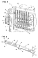
FIG. 2 is an enlarged fragmented perspective view of one end of the header connector;
FIG. 3 is a perspective view of the pin alignment plate;
FIG. 4 is an enlarged, fragmented perspective view of the left-hand end of the pin alignment plate as viewed in FIG. 3;
FIG. 5 is an enlarged, fragmented perspective view of the back side of the left-hand end of the pin alignment plate as viewed in FIG. 3;
FIG. 6 is a perspective view of the header connector, with the pin alignment plate mounted thereto in its outer or protecting position;
FIG. 7 is an enlarged, fragmented perspective view of the left-hand end of FIG. 6;
FIG. 8 is a perspective view of the header connector, with a printed circuit board mounted to the pin alignment plate and with the plate still in its outer or protecting position;
FIG. 9 is an enlarged, fragmented and sectional view of the left-hand end of FIG. 8;
FIG. 10 is an enlarged, fragmented perspective view of one end of the assembly of FIGS. 8 and 9, with the pin alignment plate and printed circuit board conjointly moved to the pin-exposing position; and,
FIG. 11 is a view similar to that of FIG. 9, but with the pin alignment plate and printed circuit board having been moved conjointly to the pin-exposing position of FIG. 10.
DETAILED DESCRIPTION OF THE PREFERRED EMBODIMENT
Referring to the drawings in greater detail, FIGS. 1 and 2 show an electrical connector in the form of a header connector, generally designated 14, which mounts a pin alignment plate, generally designated 16 in FIGS. 3-5, according to the invention. It immediately should be understood that header connector 14 is but one example of an electrical connector with which the pin alignment plate system of the invention is applicable or useful.
With that understanding, and referring first to FIG. 1, header connector 14 includes a dielectric housing, generally designated 18, which may be unitarily molded of plastic material. The housing has a pair of forwardly projecting mating portions 20 for mating with a pair of complementary mating connectors (not shown). The housing defines a rear terminating face 22 from which a pair of end wings 24 and a center wing 26 project rearwardly from terminating face 22. A cylindrical center mounting post 28 projects upwardly from center wing 26, and a pair of semi-cylindrical mounting posts 30 project upwardly from end wings 24. Mounting post 30 form relaively rigid backup members for flexible latch arms on pin alignment plate 16 as will be described in detail hereinafter.
A plurality of conductive terminals, generally designated 32, are mounted in dielectric housing 18 of header connector 14. The terminals have contact portions (not visible in the drawings) which project into mating portions 20 for engaging the terminals of the complementary mating connectors. The terminals have pin portions 32 a which project from rear terminating face 22 of housing 18 and which are bent at right angles to extend in the same direction as mounting posts 28 and 30. Pin portions 32 a of the terminals have distal ends 32 b.
Referring to FIG. 2 in conjunction with FIG. 1, a first latch boss 34 projects rearwardly from terminating face 22 of housing 18 inside each opposite end wing 24 and at opposite sides of center wing 26. This first latch boss has an upwardly facing chamfered or angled surface 34 a, as viewed in the drawings. A second latch boss 36 is formed in a groove 38 inside each end wing 24 and on opposite sides of center wing 26. This second latch boss also has an upwardly facing chamfered or angled surface 36 a. As will be seen in greater detail hereinafter, first latch bosses 34 are effective to hold pin alignment plate 16 in its outer protecting position, and second latch bosses 36 are effective to hold the pin alignment plate in its inner or pin-exposing position. Similarly, and referring to FIG. 1, a second latch boss 36, having a chamfered or angled surface 36 a, is formed on each opposite side of center wing 26.
Referring to FIGS. 3-5, pin alignment plate 16 includes an elongated plate 40 having a plurality of apertures 42 for receiving pin portions 32 a of terminals 32. Plate 40 has a center hole 44 which fits over center mounting post 28 (FIG. 1) of connector housing 18. An end notch 46 is formed at each opposite end of plate 40 for positioning over mounting posts 30 (FIG. 1) that project upwardly from end wings 24 of the connector housing. A pair of end flanges 48 project downwardly from plate 40 at opposite ends thereof, and a pair of spaced center flanges 50 project downwardly from plate 40 on opposite sides of center hole 44. As will be seen hereinafter, when pin alignment plate 16 is mounted to connector housing 18, end flanges 48 move along the insides of end wings 24 of the housing, and center flanges 50 straddle center wing 26 of the housing.
As seen best in FIG. 5, a pair of L-shaped legs 52 project inwardly from opposite edges of each end flange 48. Finally, a printed circuit board mounting post or latch arm 54 projects upwardly from each opposite end of plate 40, inside each end notch 46. Actually, the board mounting posts 54 are molded as upward extensions of end flanges 48 as best seen in FIG. 5. The board mounting posts or latch arms have inwardly projecting hooks 54 a. The entire pin alignment plate may be unitarily molded of plastic material.
Generally, first complementary interengaging latch means are provided between pin alignment plate 16 and connector housing 18 for holding the plate in an outer or protecting position as shown in FIGS. 6 and 7. This first complementary interengaging latch means include the combination of first latch bosses 34 on connector housing 18 as described above and seen best in FIG. 2, along with a pair of latch ledges 52 a defined by L-shaped legs 52 on pin alignment plate 16 as best seen in FIG. 5. This interengagement is shown clearly in FIG. 7. In other words, when pin alignment plate 16 is mounted onto connector housing 18 in the direction of arrow “A” (FIG. 7), L-shaped legs 52 of the pin alignment plate engage angled surfaces 34 a of first latch bosses 34 and ride over the latch bosses until the legs “snap” into engagement beneath the underside of the latch bosses.
This defines the outer or protecting position of the pin alignment plate as seen in FIGS. 6 and 7. In this position, board mounting posts or latch arms 54 project upwardly through end notches 46 in the plate, and semi-cylindrical end mounting posts 30 on the connector housing are positioned behind board mounting posts 54. It can be seen in FIG. 7 that distal ends 32 b of terminal pin portions 32 a project into holes 42 in the pin alignment plate but do not project completely therethrough. In this outer position of the pin alignment plate, the pin portions are properly spaced, aligned and protected.
After pin alignment plate 16 is positioned on connector housing 18 in its outer or protecting position shown in FIGS. 6 and 7, a printed circuit board 60 then can be mounted onto the pin alignment plate as seen in FIGS. 8 and 9. The printed circuit board has a plurality of holes 62 through which pin portions 32 a of terminals 32 are to be inserted for connection to appropriate circuit traces (not shown) on the board and/or in the holes. When the board is mounted on the pin alignment plate, holes 62 in the board are aligned with holes 42 in the plate. The board has a center mounting hole 64 (FIG. 8) for receiving center mounting post 28 (FIG. 1) of the connector housing. The board has a pair of end mounting holes 66 for receiving both mounting posts or latch arms 54 of the pin alignment plate as well as end mounting posts 30 of the connector housing.
When the circuit board is mounted on top of pin alignment plate 16, hooks 54 a of latch arms 54 snap into engagement with the top surface of the board. With the pin alignment plate being molded of plastic material, mounting posts 54 are flexible and they perform a dual function of forming flexible latch arms for securing the printed circuit board to the top of the pin alignment plate.
After printed circuit board 60 is mounted to pin alignment plate 16 as described above, both the board and the plate are conjointly movable to a pin-exposing position shown in FIGS. 10 and 11. Generally, second complementary interengaging latch means are provided between the pin alignment plate and the housing for holding the plate in this pin-exposing position. Specifically, referring back to FIG. 5, a latch boss 70 is formed on the outside of each end flange 48 of pin alignment plate 16. The latch boss has a leading (in the direction of movement) angled surface 70 a and a trailing, abrupt latch surface 70 b. Latch bosses 70 on the pin alignment plate cooperate with second latch bosses 36 on the connector housing as described above in relation to FIG. 2, to define the second complementary interengaging latch means for holding the alignment plate in its pin-exposing position as shown in FIGS. 10 and 11.
This interengagement is seen clearly in FIG. 11 where latch surface 70 b of one of the latch bosses 70 on pin alignment plate 16 is shown engaged with the bottom of one of the latch bosses 36 on the connector housing. During movement of the pin alignment plate and printed circuit board to the pin-exposing position, leading angled surfaces 70 a of latch bosses 70 engage angled surfaces 36 a of latch bosses 36 as the pin alignment plate moves in the direction of arrow “B” (FIG. 11). This causes latch bosses 70 on flanges 58 to ride over latch bosses 36 and snap into interengagement as seen in FIG. 11.
FIG. 11 also shows that semi-cylindrical end mounting posts 30 on connector housing 18 move into a position behind board mounting posts or flexible latch arms 54 of the pin alignment plate. This prevents hooks 54 a of flexible latch arms 54 from moving out of securing engagement with the top surface of printed circuit board 60. In this pin-exposing position of the pin alignment plate and the circuit board, it can be seen in both FIGS. 10 and 11 that distal ends 32 b of pin portions 32 project completely through holes 62 in circuit board 60. The pin portions now can be electrically connected to appropriate circuit traces on the board and/or in the holes.
Angled surfaces 70 a of latch bosses 70 as described above in relation to FIGS. 5 and 11, also perform an abutting function to further define the outer protecting position of pin alignment plate 16. This is seen in FIG. 9 wherein angled surface 70 a abuts against angled surface 36 a of second latch boss 36 on the connector housing. In FIG. 9, it can be seen that first latch boss 34 is in engagement with latch surface 52 a while angled surfaces 36 a and 70 a are in interengagement. This positively defines the outer or protecting position of the pin alignment plate and printed circuit board in opposite directions. When the pin alignment plate and printed circuit board are moved to the inner pin-exposing position of FIGS. 10 and 11, the pin alignment plate abuts the top surfaces of end wings 24 and center wing 26 (FIG. 1).
The invention has a variety of applications. For instance, certain manufacturers may manufacture electrical connectors while other manufacturers manufacture printed circuit boards. With the invention, electrical connector 14 can be manufactured with pin alignment plate 16 mounted thereto for protecting pin portions 32 a of terminals 32 during handling and transit. Printed circuit board 60 subsequently can be added to this combination, with both the circuit board and the pin alignment plate still in its pin-protecting position. During further handling to other processing stations, such as a reflow soldering processing station for electrically connecting the pin portions of the terminals to the circuit traces on the printed circuit board, the board and pin alignment plate can remain in the protecting position until it is necessary to expose the distal ends of the pin portions for ultimate processing. In addition, it often is difficult to insert terminal pins into holes in printed circuit boards without making the holes in the board unduly large. With the invention, the holes in pin alignment plate 16 can be chamfered for easy insertion of the distal ends of the pin portions thereinto and to prealign the distal ends of the pin portions with the holes in the printed circuit board which can be precisely mounted to the top of the pin alignment plate.
It will be understood that the invention may be embodied in other specific forms without departing from the spirit or central characteristics thereof. The present examples and embodiments, therefore, are to be considered in all respects as illustrative and not restrictive, and the invention is not to be limited to the details given herein.

Claims (22)

1. An electrical connector, comprising:
dielectric housing;
plurality of conductive terminals mounted on the housing with pin portions projecting therefrom; and
a pin alignment plate having a plurality of apertures for receiving the pin portions of the terminals, the pin alignment plate being movably mounted on the housing for movement from an outer protecting position generally at distal ends of said pin portions to an inner pin-exposing position spaced inwardly of said distal ends, and said pin alignment plate having mounting means for fixing a printed circuit board thereon in the outer protecting position of the alignment plate for movement inwardly therewith between said positions.
2. The electrical connector of claim 1, further including complementary interengaging latch means between said pin alignment plate and said housing for holding said pin alignment plate in said protecting position.
3. The electrical connector of claim 1, further including complementary interengaging latch means between aid pin alignment plate and said housing for holding said pin alignment plate in said pin-exposing position.
4. The electrical connector of claim 3, further including additional complementary interengaging latch means between said pin alignment plate and said housing for holding said pin alignment plate in said protecting position.
5. In combination with the electrical connector of claim 1, a printed circuit board having complementary mounting means for cooperating with said mounting means on said pin alignment plate to facilitate mounting the printed circuit board on said pin alignment plate.
6. The combination of claim 5, wherein said mounting means on said pin alignment plate comprise at least one latch arm, and the complementary mounting means on the printed circuit board comprise a hole for receiving the latch arm.
7. The electrical connector of claim 1, wherein said mounting means comprises at least one arm for projecting through a mounting hole in said printed circuit board.
8. The electrical connector of claim 7, wherein said arm is a latch arm and is flexible for resiliently latchingly engaging said printed circuit board, and said housing includes a relatively rigid backup member for positioning behind the latch arm to prevent said latch arm from flexing out of latching engagement with said printed circuit board when said pin alignment plate is in said pin-exposing position.
9. The electrical connector of claim 7, wherein said arm is flexible and includes a hook portion for snapping into latching engagement with one side of said printed circuit board as said arm is inserted through the mounting hole in said printed circuit board.
10. The electrical connector of claim 9, wherein said housing includes a relatively rigid backup member for positioning behind said arm to prevent said arm from flexing out of engagement with said printed circuit board when said pin alignment plate is in said pin-exposing position.
11. An electrical connector, comprising:
a dielectric housing;
a plurality of conductive terminals mounted on the housing with pin portions projecting therefrom;
a pin alignment plate having a plurality of apertures for receiving the pin portions of the terminals, the pin alignment plate being movably mounted on the housing for movement from an outer protecting position generally at distal ends of said pin portions to an inner pin-exposing position spaced inwardly of said distal ends, and said pin alignment plate having at least one latch arm for projecting through a mounting hole in a printed circuit board to latch the printed circuit board to said pin alignment plate in the outer protecting position of the alignment plate for movement inwardly therewith between said positions;
first complementary interengaging latch means between aid pin alignment plate and said housing for holding said pin alignment plate in said protecting position; and,
second complementary interengaging latch means between said pin alignment plate and said housing for holding said pin alignment plate in said pin-exposing position.
12. The electrical connector of claim 11, wherein said latch arm is flexible and includes a hook portion for snapping into latching engagement with one side of said printed circuit board as said latch arm is inserted through the mounting hole in said printed circuit board.
13. The electrical connector of claim 12, wherein said housing includes a relatively rigid backup member for positioning behind said latch arm to prevent said latch arm from flexing out of engagement with said printed circuit board when said pin alignment plate is in said pin-exposing position.
14. The electrical connector of claim 11, wherein said latch arm is flexible for resiliently latchingly engaging said printed circuit board, and said housing includes a relatively rigid backup member for positioning behind said latch arm to prevent said latch arm from flexing out of latching engagement with said printed circuit board when said pin alignment plate is in said pin-exposing position.
15. The electrical connector of claim 14, wherein said housing includes a mounting post for projecting through a mounting hole in said pin alignment plate, said mounting post performing a dual function of comprising said backup member for positioning behind said flexible latch arm.
16. In combination with the electrical connector of claim 11, a printed circuit board having complementary mounting means for cooperating with said mounting means on said pin alignment plate to facilitate mounting said printed circuit board on said pin alignment plate.
17. In combination of claim 16, wherein said mounting means on said pin alignment plate comprise at least one latch arm, and the complementary mounting means on said printed circuit board comprise a hole for receiving said latch.
18. An electrical connector, comprising:
a dielectric housing;
a plurality of conductive terminals mounted on the housing with pin portions projecting therefrom;
a pin alignment plate having a plurality of apertures for receiving the pin portions of the terminals, the pin alignment plate being movably mounted on the housing for movement from a protecting position generally at distal ends of said pin portions to a pin-exposing position spaced inwardly of said distal ends, and said pin alignment plate having mounting means for mounting a printed circuit board thereon for movement therewith between said positions, said mounting means comprising at least one flexible arm for projecting through a mounting hole in said printed circuit board, the flexible arm including a hook portion for snapping into latching engagement with one side of said printed circuit board as said arm is inserted through the mounting hole in said printed circuit board; and
said housing including a relatively rigid backup member for positioning behind said flexible arm to prevent said arm from flexing out of engagement with said printed circuit board when said pin alignment plate is in said pin-exposing position.
19. An electrical connector, comprising:
a dielectric housing;
a plurality of conductive terminals mounted on the housing with pin portions projecting therefrom;
a pin alignment plate having a plurality of apertures for receiving the pin portions of the terminals, the pin alignment plate being movably mounted on the housing for movement from a protecting position generally at distal ends of said pin portions to a pin-exposing position spaced inwardly of said distal ends, and said pin alignment plate having mounting means for mounting a printed circuit board thereon for movement therewith between said positions, said mounting means comprising at least one flexible latch arm for resiliently latchingly engaging said printed circuit board; and
said housing including a relatively rigid backup member for positioning behind the flexible latch arm to prevent said latch arm from flexing out of latching engagement with said printed circuit board when said pin alignment plate is in said pin-exposing position.
20. An electrical connector, comprising:
a dielectric housing;
a plurality of conductive terminals mounted on the housing with pin portions projecting therefrom;
a pin alignment plate having a plurality of apertures for receiving the pin portions of the terminals, the pin alignment plate being movably mounted on the housing for movement from a protecting position generally at distal ends of said pin portions to a pin-exposing position spaced inwardly of said distal ends, and said pin alignment plate having at least one latch arm for projecting through a mounting hole in a printed circuit board to mount the printed circuit board on said pin alignment plate for movement therewith between said positions, said latch arm being flexible and including a hook portion for snapping into latching engagement with one side of said printed circuit board as said latch arm is inserted through the mounting hole in said printed circuit board;
first complementary interengaging latch means between aid pin alignment plate and said housing for holding said pin alignment plate in said protecting position;
second complementary interengaging latch means between said pin alignment plate and said housing for holding said pin alignment plate in said pin-exposing position; and
said housing including a relatively rigid backup member for positioning behind said latch arm to prevent said latch arm from flexing out of engagement with said printed circuit board when said pin alignment plate is in said pin-exposing position.
21. An electrical connector, comprising:
a dielectric housing;
a plurality of conductive terminals mounted on the housing with pin portions projecting therefrom;
a pin alignment plate having a plurality of apertures for receiving the pin portions of the terminals, the pin alignment plate being movably mounted on the housing for movement from a protecting position generally at distal ends of said pin portions to a pin-exposing position spaced inwardly of said distal ends, and said pin alignment plate having at least one latch arm for projecting through a mounting hole in a printed circuit board to mount the printed circuit board on said pin alignment plate for movement therewith between said positions, said latch arm being flexible for resiliently latchingly engaging said printed circuit board;
first complementary interengaging latch means between aid pin alignment plate and said housing for holding said pin alignment plate in said protecting position;
second complementary interengaging latch means between said pin alignment plate and said housing for holding said pin alignment plate in said pin-exposing position; and
said housing including a relatively rigid backup member for positioning behind said latch arm to prevent said latch arm from flexing out of latching engagement with said printed circuit board when said pin alignment plate is in said pin-exposing position.
22. An electrical connector of claim 21, wherein said housing includes a mounting post for projecting through a mounting hole in said pin alignment plate, said mounting post performing a dual function of comprising said backup member for positioning behind said flexible latch arm.
US10/374,964 2003-02-21 2003-02-21 Electrical connector with a terminal pin alignment plate Expired - Lifetime US6866552B2 (en)

Priority Applications (1)

Application Number Priority Date Filing Date Title
US10/374,964 US6866552B2 (en) 2003-02-21 2003-02-21 Electrical connector with a terminal pin alignment plate

Applications Claiming Priority (1)

Application Number Priority Date Filing Date Title
US10/374,964 US6866552B2 (en) 2003-02-21 2003-02-21 Electrical connector with a terminal pin alignment plate

Publications (2)

Publication Number Publication Date
US20040166705A1 US20040166705A1 (en) 2004-08-26
US6866552B2 true US6866552B2 (en) 2005-03-15

Family

ID=32868993

Family Applications (1)

Application Number Title Priority Date Filing Date
US10/374,964 Expired - Lifetime US6866552B2 (en) 2003-02-21 2003-02-21 Electrical connector with a terminal pin alignment plate

Country Status (1)

Country Link
US (1) US6866552B2 (en)

Cited By (15)

* Cited by examiner, † Cited by third party
Publication number Priority date Publication date Assignee Title
US20060019515A1 (en) * 2004-07-21 2006-01-26 J.S.T. Mfg. Co., Ltd. Connector
US20060134975A1 (en) * 2004-12-21 2006-06-22 J.S.T. Corporation Electrical connector with a tine plate
US7080990B1 (en) * 2005-02-09 2006-07-25 Hon Hai Precision Ind. Co., Ltd. Control module assembly
US7094075B1 (en) * 2005-06-15 2006-08-22 Mea Technologies Pte. Ltd. Electrical connector with a detachable hood
US20060205264A1 (en) * 2005-03-14 2006-09-14 Sumitomo Wiring Systems, Ltd. Connector
US20090035983A1 (en) * 2007-07-31 2009-02-05 Phoenix Contact Development & Manufacturing, Inc. Modular terminal block
US20090111293A1 (en) * 2007-10-29 2009-04-30 Brandon Rubenstein Retractable protection apparatus for electronic device pins
US20090263987A1 (en) * 2008-04-21 2009-10-22 Hon Hai Precision Ind.Co., Ltd. Burn-in socket having protecting device
US20100041255A1 (en) * 2006-11-02 2010-02-18 Molex Incorporated Substrate Connector
US20110171840A1 (en) * 2007-12-27 2011-07-14 Tooru Sakai Semiconductor device socket
US20110281462A1 (en) * 2010-05-13 2011-11-17 Sumitomo Wiring Systems, Ltd. Board connector and method of mounting it
US20180370460A1 (en) * 2017-06-21 2018-12-27 Yazaki Corporation Electronic component unit, wire harness, and connector fixing structure
US10312626B2 (en) 2017-06-30 2019-06-04 Te Connectivity Corporation Electrical connector with terminal alignment plate and secondary lock detection
US11251575B2 (en) 2020-07-09 2022-02-15 Rockwell Automation Technologies, Inc. Connector alignment and retention panel for modular based system
US11381024B2 (en) 2020-02-26 2022-07-05 Foxconn (Kunshan) Computer Connector Co., Ltd. Electrical connector

Families Citing this family (5)

* Cited by examiner, † Cited by third party
Publication number Priority date Publication date Assignee Title
US7278856B2 (en) * 2004-08-31 2007-10-09 Fci Americas Technology, Inc. Contact protector for electrical connectors
JP6325880B2 (en) * 2014-04-24 2018-05-16 矢崎総業株式会社 connector
DE112015001910T5 (en) * 2014-04-24 2017-01-19 Yazaki Corporation Interconnects
JP6738245B2 (en) * 2016-09-02 2020-08-12 タイコエレクトロニクスジャパン合同会社 Electrical connector
EP3932155A1 (en) * 2019-02-27 2022-01-05 Robert Bosch GmbH An electronic control module (ecm) and mounting arrangement of a guide plate in the ecm

Citations (3)

* Cited by examiner, † Cited by third party
Publication number Priority date Publication date Assignee Title
US4717217A (en) * 1980-02-12 1988-01-05 Virginia Patent Development Corporation Connector for mating modular plug with printed circuit board
US5078626A (en) * 1989-11-14 1992-01-07 Yamaichi Electric Mfg. Co., Ltd. Connector for electric parts
US5591036A (en) * 1994-02-21 1997-01-07 Kel Corporation Circuit board connector

Patent Citations (3)

* Cited by examiner, † Cited by third party
Publication number Priority date Publication date Assignee Title
US4717217A (en) * 1980-02-12 1988-01-05 Virginia Patent Development Corporation Connector for mating modular plug with printed circuit board
US5078626A (en) * 1989-11-14 1992-01-07 Yamaichi Electric Mfg. Co., Ltd. Connector for electric parts
US5591036A (en) * 1994-02-21 1997-01-07 Kel Corporation Circuit board connector

Cited By (28)

* Cited by examiner, † Cited by third party
Publication number Priority date Publication date Assignee Title
US20060019515A1 (en) * 2004-07-21 2006-01-26 J.S.T. Mfg. Co., Ltd. Connector
US7303408B2 (en) * 2004-07-21 2007-12-04 J.S.T. Manufacturing Co., Ltd. Connector
US20060134975A1 (en) * 2004-12-21 2006-06-22 J.S.T. Corporation Electrical connector with a tine plate
US7214074B2 (en) * 2004-12-21 2007-05-08 J.S.T. Corporation Electrical connector with a tine plate
US7080990B1 (en) * 2005-02-09 2006-07-25 Hon Hai Precision Ind. Co., Ltd. Control module assembly
US20060177960A1 (en) * 2005-02-09 2006-08-10 Hon Hai Precision Ind. Co., Ltd. Control module assembly
US20060205264A1 (en) * 2005-03-14 2006-09-14 Sumitomo Wiring Systems, Ltd. Connector
US7267562B2 (en) * 2005-03-14 2007-09-11 Sumitomo Wiring Systems, Ltd. Connector
US7094075B1 (en) * 2005-06-15 2006-08-22 Mea Technologies Pte. Ltd. Electrical connector with a detachable hood
US20100041255A1 (en) * 2006-11-02 2010-02-18 Molex Incorporated Substrate Connector
US7938651B2 (en) * 2006-11-02 2011-05-10 Molex Incorporated Substrate connector
US20090035983A1 (en) * 2007-07-31 2009-02-05 Phoenix Contact Development & Manufacturing, Inc. Modular terminal block
US7491096B1 (en) 2007-07-31 2009-02-17 Phoenix Contact Development & Manufacturing Inc. Modular terminal block
US20090111293A1 (en) * 2007-10-29 2009-04-30 Brandon Rubenstein Retractable protection apparatus for electronic device pins
US7544072B2 (en) 2007-10-29 2009-06-09 Hewlett-Packard Development Company, L.P. Retractable protection apparatus for electronic device pins
US8272882B2 (en) * 2007-12-27 2012-09-25 Yamaichi Electronics Co., Ltd. Semiconductor device socket
US20110171840A1 (en) * 2007-12-27 2011-07-14 Tooru Sakai Semiconductor device socket
US20090263987A1 (en) * 2008-04-21 2009-10-22 Hon Hai Precision Ind.Co., Ltd. Burn-in socket having protecting device
US7708572B2 (en) * 2008-04-21 2010-05-04 Hon Hai Precision Ind. Co. Ltd. Burn-in socket having protecting device
US20110281462A1 (en) * 2010-05-13 2011-11-17 Sumitomo Wiring Systems, Ltd. Board connector and method of mounting it
US8435051B2 (en) * 2010-05-13 2013-05-07 Sumitomo Wiring Systems, Ltd. Board connector and method of mounting it
US20180370460A1 (en) * 2017-06-21 2018-12-27 Yazaki Corporation Electronic component unit, wire harness, and connector fixing structure
JP2019008918A (en) * 2017-06-21 2019-01-17 矢崎総業株式会社 Electronic component unit, wiring harness, and connector fixing structure
US10513231B2 (en) * 2017-06-21 2019-12-24 Yazaki Corporation Electronic component unit, wire harness, and connector fixing structure
US10312626B2 (en) 2017-06-30 2019-06-04 Te Connectivity Corporation Electrical connector with terminal alignment plate and secondary lock detection
US11381024B2 (en) 2020-02-26 2022-07-05 Foxconn (Kunshan) Computer Connector Co., Ltd. Electrical connector
US11251575B2 (en) 2020-07-09 2022-02-15 Rockwell Automation Technologies, Inc. Connector alignment and retention panel for modular based system
US11777261B2 (en) 2020-07-09 2023-10-03 Rockwell Automation Technologies, Inc. Connector alignment and retention panel for modular based system

Also Published As

Publication number Publication date
US20040166705A1 (en) 2004-08-26

Similar Documents

Publication Publication Date Title
US6866552B2 (en) Electrical connector with a terminal pin alignment plate
US20200259294A1 (en) Robust, compact electrical connector
EP1026785B1 (en) Adapter frame assembly for electrical connectors
US6773272B2 (en) Electrical connector assembly and module incorporating the same
EP1026784B1 (en) Shielded electrical connector
US7320605B2 (en) Board-to-board connector with improved terminal contacts
US5257948A (en) Printed circuit board mounting device for electrical connectors
US6146184A (en) Circuit board mounted connector assembly and method of fabricating same
US5310360A (en) Circuit board mounted modular phone jack
US6315620B1 (en) System, method, and device for a pre-loaded straddle mounted connector assembly
EP0749182A1 (en) Electrical connector with terminal tail aligning device
US6482032B1 (en) Electrical connector with board locks
EP0635909A1 (en) Printed circuit board electrical connector with mounting latch clip
US7011548B2 (en) Board mounted side-entry electrical connector
US6135816A (en) Electrical connector having an improved construction for fixing shield plates to a receptacle connector
US7059915B1 (en) Panel mounted modular jack terminated to a circuit board
US6244887B1 (en) Electrical connector assembly
US6361332B1 (en) Retention system for electrical connectors
WO2005107022A1 (en) : board mounted electrical connector assembly
US6790052B2 (en) Circuit board straddle mounted connector
US6287129B1 (en) Card connector assembly
EP3465827A1 (en) Poke-in electrical connector
US6733310B2 (en) Electrical connector with improved electrostatic discharge system
JP3898643B2 (en) Small board to board connector
US6830485B2 (en) Electrical connector with a terminal pin stabilizing plate

Legal Events

Date Code Title Description
AS Assignment

Owner name: MOLEX INCORPORATED, ILLINOIS

Free format text: ASSIGNMENT OF ASSIGNORS INTEREST;ASSIGNOR:KOEHLER, DAVID F.;REEL/FRAME:013817/0014

Effective date: 20030217

STCF Information on status: patent grant

Free format text: PATENTED CASE

FPAY Fee payment

Year of fee payment: 4

FPAY Fee payment

Year of fee payment: 8

FPAY Fee payment

Year of fee payment: 12

AS Assignment

Owner name: MOLEX, LLC, ILLINOIS

Free format text: CHANGE OF NAME;ASSIGNOR:MOLEX INCORPORATED;REEL/FRAME:062820/0197

Effective date: 20150819