US6759986B1 - Stacked patch antenna - Google Patents
Stacked patch antenna Download PDFInfo
- Publication number
- US6759986B1 US6759986B1 US10/146,609 US14660902A US6759986B1 US 6759986 B1 US6759986 B1 US 6759986B1 US 14660902 A US14660902 A US 14660902A US 6759986 B1 US6759986 B1 US 6759986B1
- Authority
- US
- United States
- Prior art keywords
- passive
- antenna element
- driven
- antenna
- opposing surface
- Prior art date
- Legal status (The legal status is an assumption and is not a legal conclusion. Google has not performed a legal analysis and makes no representation as to the accuracy of the status listed.)
- Expired - Lifetime
Links
- 239000000758 substrate Substances 0.000 claims abstract description 15
- 238000000034 method Methods 0.000 claims description 10
- 239000000853 adhesive Substances 0.000 claims description 4
- 230000001070 adhesive effect Effects 0.000 claims description 4
- 229920001940 conductive polymer Polymers 0.000 claims description 4
- 239000004417 polycarbonate Substances 0.000 claims description 4
- 229920000515 polycarbonate Polymers 0.000 claims description 4
- 238000000926 separation method Methods 0.000 claims description 3
- 230000003071 parasitic effect Effects 0.000 abstract description 14
- 238000004519 manufacturing process Methods 0.000 description 6
- 229920004142 LEXAN™ Polymers 0.000 description 2
- 239000004418 Lexan Substances 0.000 description 2
- 239000000463 material Substances 0.000 description 2
- 238000010561 standard procedure Methods 0.000 description 2
- RRKGBEPNZRCDAP-UHFFFAOYSA-N [C].[Ag] Chemical compound [C].[Ag] RRKGBEPNZRCDAP-UHFFFAOYSA-N 0.000 description 1
- 230000005540 biological transmission Effects 0.000 description 1
- 238000010276 construction Methods 0.000 description 1
- 230000008878 coupling Effects 0.000 description 1
- 238000010168 coupling process Methods 0.000 description 1
- 238000005859 coupling reaction Methods 0.000 description 1
- 238000005530 etching Methods 0.000 description 1
- 238000012986 modification Methods 0.000 description 1
- 230000004048 modification Effects 0.000 description 1
- 239000004033 plastic Substances 0.000 description 1
- 238000012216 screening Methods 0.000 description 1
Images

Classifications
-
- H—ELECTRICITY
- H01—ELECTRIC ELEMENTS
- H01Q—ANTENNAS, i.e. RADIO AERIALS
- H01Q9/00—Electrically-short antennas having dimensions not more than twice the operating wavelength and consisting of conductive active radiating elements
- H01Q9/04—Resonant antennas
- H01Q9/0407—Substantially flat resonant element parallel to ground plane, e.g. patch antenna
- H01Q9/0414—Substantially flat resonant element parallel to ground plane, e.g. patch antenna in a stacked or folded configuration
Definitions
- the present invention is directed to the field of antennas, particularly patch antennas of the type used for wireless telecommunications devices.
- a simple patch antenna has a very small VSWR bandwidth, 0.7%-1.5% (where VSWR indicates “Voltage Standing Wave Ratio”).
- a parasitic patch element can be deployed above a driven patch element. This is called a “stacked patch” antenna.
- the parasitic element increases the capacitance of the driven antenna element, thereby increasing the bandwidth of the antenna system.
- the separation between the driven element and the parasitic element contributes to the VSWR bandwidth and the antenna gain.
- a parasitic element is etched onto a rigid circuit board using standard techniques for manufacturing printed circuit boards.
- the parasitic element is then typically mounted above a driven antenna element, which is also typically etched onto a rigid circuit board using standard techniques for manufacturing printed circuit boards.
- This type of construction can be expensive since several manufacturing steps are required to produce the parasitic element in the proper relation to the driven element.
- the placement and separation between the elements is critical in realizing the desired bandwidth results. This can be hard to control using previous-type techniques, thereby adding to the cost of manufacture.
- the present stacked patch antenna includes a first antenna element and a second antenna element for cooperating with the first antenna element. These antenna elements are preferably a passive parasitic element in combination with a driven element.
- a flexible substrate is provided having first and second opposing surfaces, each respectively in contact with the second (parasitic) antenna element.
- the flexible substrate preferably has a desired dielectric property to provide the desired coupling between the antenna elements.
- One or both of the antenna elements are formed on the respective opposing surface.
- the antenna element is preferably formed by printing.
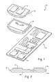
- FIG. 1 is an exploded view showing the present antenna assembly included in a wireless radio device.
- FIG. 2 is a side sectional view showing the layers of the parasitic antenna used with the present invention.
- a stacked patch antenna 10 having a first antenna element and a second antenna element for cooperating with the first antenna element.
- the first antenna element is a passive antenna element 12 , e.g., a parasitic patch element and the second antenna element is a driven antenna element 14 in connection with a ratio circuit 16 , preferably a circuit of the type used to communicate over a Wireless Local Area Network (WLAN) in the 2.4 GHz or 5 GHz wireless bands in accordance with the IEEE 802.11 protocols.
- WLAN Wireless Local Area Network
- the driven element 14 can be formed on a printed circuit board using standard PCB etching techniques, preferably the same board as the radio circuit 16 .
- PCB etching techniques preferably the same board as the radio circuit 16 .
- the invention is not limited to the particular wireless implementation and could be easily adapted without departing from the invention.
- one ore more pairs of antenna elements 12 , 14 can be deployed without departing from the invention.
- a flexible substrate 20 is provided having first and second opposing surfaces 22 , 24 .
- Passive antenna elements 12 can be formed on a respective opposing surface 22 , 24 .
- the passive antenna element 12 is formed on the first opposing surface 22 .
- the second opposing surface 24 is affixed in a spaced relationship to the driven antenna element 14 .
- an intermediate mounting member can be provided, to which the second opposing surface is affixed, for defining the spaced relationship between the antenna elements 12 , 14 .
- the intermediate mounting member is preferably a radome 26 , a plastic housing portion for enclosing the driven antenna element 14 .
- the intermediate mounting member may be formed integrally with the flexible substrate 20 , of sufficient thickness to provide the necessary spaced relationship.
- the intermediate mounting member has predetermined dielectric properties so as to provide a predetermined capacitance between the antenna elements. This configuration thereby allows a VSWR bandwidth of at least 5%, thereby providing a significant improvement in wireless transmission and reception efficiency.
- the second opposing surface 24 of the flexible substrate 20 includes an adhesive 28 for affixing the driven antenna element 14 .
- the flexible substrate 20 is preferably formed of polycarbonate, such as the product sold under the name “Lexan” by General Electric Company of Schenectady, N.Y.
- the parasitic element 12 can be formed of highly conductive polymer thick film such as Dupont Silver Carbon 5524.
- the passive antenna 12 is printed onto a Lexan “sticker” or “decal” using standard printing techniques, e.g., silk screening, etc. The “sticker” is then affixed in the proper position at the required spacing above the driven elements.
- the decal can include decorative or descriptive indicia printed over the top surface of the antenna element 12 . This provides protection for the antenna element and provides a location for the placement of a logo, etc.
- the present method and apparatus provides considerable reduction in manufacturing and material usage over previous-type implementations, resulting in considerable reduction in production expense. Also, the use of a printed conductive thick film allows extremely close control over the physical dimensions of the parasitic element. Finally, the use of the “decal” allows for accurate positioning of the parasitic antenna elements in all directions.
- the present invention can be deployed in radio circuits 16 used in client devices and also in stationary network access point devices.
Abstract
A stacked patch antenna is disclosed which includes a first antenna element and a second antenna element for cooperating with the first antenna element. These antenna elements are preferably a passive parasitic element in combination with a driven element. A flexible substrate is provided having first and second opposing surfaces, each respectively in contact with the first and second antenna elements. The flexible substrate preferably has a desired dielectric property to provide a desired capacitance between the antenna elements. One or both of the antenna elements are formed on the respective opposing surface. The antenna element is preferably formed by printing.
Description
The present invention is directed to the field of antennas, particularly patch antennas of the type used for wireless telecommunications devices. A simple patch antenna has a very small VSWR bandwidth, 0.7%-1.5% (where VSWR indicates “Voltage Standing Wave Ratio”). In order to increase the VSWR bandwidth of a patch antenna, a parasitic patch element can be deployed above a driven patch element. This is called a “stacked patch” antenna. The parasitic element increases the capacitance of the driven antenna element, thereby increasing the bandwidth of the antenna system. The separation between the driven element and the parasitic element contributes to the VSWR bandwidth and the antenna gain.
In a common stacked antenna arrangement, a parasitic element is etched onto a rigid circuit board using standard techniques for manufacturing printed circuit boards. The parasitic element is then typically mounted above a driven antenna element, which is also typically etched onto a rigid circuit board using standard techniques for manufacturing printed circuit boards. This type of construction can be expensive since several manufacturing steps are required to produce the parasitic element in the proper relation to the driven element. Also, the placement and separation between the elements is critical in realizing the desired bandwidth results. This can be hard to control using previous-type techniques, thereby adding to the cost of manufacture.
The difficulties and drawbacks of previous-type deployments are overcome by the method and apparatus of the present invention. The present stacked patch antenna includes a first antenna element and a second antenna element for cooperating with the first antenna element. These antenna elements are preferably a passive parasitic element in combination with a driven element. A flexible substrate is provided having first and second opposing surfaces, each respectively in contact with the second (parasitic) antenna element. The flexible substrate preferably has a desired dielectric property to provide the desired coupling between the antenna elements. One or both of the antenna elements are formed on the respective opposing surface. The antenna element is preferably formed by printing.
As will be realized, the invention is capable of other and different embodiments and its several details are capable of modifications in various respects, all without departing from the invention. Accordingly, the drawing and description are to be regarded as illustrative and not restrictive.
FIG. 1 is an exploded view showing the present antenna assembly included in a wireless radio device.
FIG. 2 is a side sectional view showing the layers of the parasitic antenna used with the present invention.
An exemplary embodiment of the invention is disclosed in the figures, where like reference numerals are understood to refer to like elements. As shown in FIGS. 1 and 2, a stacked patch antenna 10 is disclosed having a first antenna element and a second antenna element for cooperating with the first antenna element. In the preferred embodiment, the first antenna element is a passive antenna element 12, e.g., a parasitic patch element and the second antenna element is a driven antenna element 14 in connection with a ratio circuit 16, preferably a circuit of the type used to communicate over a Wireless Local Area Network (WLAN) in the 2.4 GHz or 5 GHz wireless bands in accordance with the IEEE 802.11 protocols. The driven element 14 can be formed on a printed circuit board using standard PCB etching techniques, preferably the same board as the radio circuit 16. Of course, it is appreciated that the invention is not limited to the particular wireless implementation and could be easily adapted without departing from the invention. As shown, one ore more pairs of antenna elements 12, 14 can be deployed without departing from the invention.
A flexible substrate 20 is provided having first and second opposing surfaces 22, 24. Passive antenna elements 12, can be formed on a respective opposing surface 22, 24. In the illustrated embodiment, the passive antenna element 12 is formed on the first opposing surface 22. The second opposing surface 24 is affixed in a spaced relationship to the driven antenna element 14. In the preferred embodiment, an intermediate mounting member can be provided, to which the second opposing surface is affixed, for defining the spaced relationship between the antenna elements 12, 14. The intermediate mounting member is preferably a radome 26, a plastic housing portion for enclosing the driven antenna element 14. It may also be contemplated that the intermediate mounting member may be formed integrally with the flexible substrate 20, of sufficient thickness to provide the necessary spaced relationship. In any case, the intermediate mounting member has predetermined dielectric properties so as to provide a predetermined capacitance between the antenna elements. This configuration thereby allows a VSWR bandwidth of at least 5%, thereby providing a significant improvement in wireless transmission and reception efficiency.
In the preferred embodiment, the second opposing surface 24 of the flexible substrate 20 includes an adhesive 28 for affixing the driven antenna element 14. The flexible substrate 20 is preferably formed of polycarbonate, such as the product sold under the name “Lexan” by General Electric Company of Schenectady, N.Y. Preferably, the parasitic element 12 can be formed of highly conductive polymer thick film such as Dupont Silver Carbon 5524. Preferably, the passive antenna 12 is printed onto a Lexan “sticker” or “decal” using standard printing techniques, e.g., silk screening, etc. The “sticker” is then affixed in the proper position at the required spacing above the driven elements. The decal can include decorative or descriptive indicia printed over the top surface of the antenna element 12. This provides protection for the antenna element and provides a location for the placement of a logo, etc.
The present method and apparatus provides considerable reduction in manufacturing and material usage over previous-type implementations, resulting in considerable reduction in production expense. Also, the use of a printed conductive thick film allows extremely close control over the physical dimensions of the parasitic element. Finally, the use of the “decal” allows for accurate positioning of the parasitic antenna elements in all directions. The present invention can be deployed in radio circuits 16 used in client devices and also in stationary network access point devices.
As described hereinabove, the present invention solves many problems associated with previous type devices. However, it will be appreciated that various changes in the details, materials and arrangements of parts which have been herein described and illustrated in order to explain the nature of the invention may be made by those skilled in the area within the principle and scope of the invention will be expressed in the appended claims.
Claims (16)
1. A stacked patch antenna comprising:
a passive antenna element;
a driven antenna element formed on a printed circuit board in connection with a radio circuit for cooperating with the passive antenna element;
a flexible substrate having first and second opposing surfaces wherein the passive antenna element is formed on the first opposing surface and wherein the second opposing surface comprises an adhesive for affixing in a spaced relationship to the driven antenna element.
2. The stacked patch antenna of claim 1 further comprising an intermediate mounting member, to which the second opposing surface is affixed, for defining the spaced relationship between the passive and driven antenna elements, wherein the intermediate mounting member has predetermined dielectric properties so as to provide a predetermined capacitance between the passive and driven antenna elements.
3. The stacked patch antenna of claim 1 wherein the flexible substrate is formed of polycarbonate.
4. The stacked patch antenna of claim 1 wherein at least one of the passive and driven antenna elements is formed of a conductive polymer.
5. A method of forming a stacked patch antenna comprising:
forming a driven antenna element onto a printed circuit board connected to a radio circuit;
providing a flexible substrate having first and second opposing surfaces for defining a predetermined separation;
forming a passive antenna element to the first opposing surface;
adhering a driven antenna element in a spaced relationship to the second opposing surface with an adhesive.
6. The method of claim 5 wherein the step of affixing comprises affixing to an intermediate mounting member, for defining the spaced relationship between the passive and driven antenna elements, wherein the intermediate mounting member is selected to have predetermined dielectric properties so as to provide a predetermined capacitance between the passive and driven antenna elements.
7. The method of claim 5 wherein the step of providing the flexible substrate comprises forming the flexible substrate of polycarbonate.
8. The method of claim 5 wherein the step of forming comprises printing the passive antenna element onto the first opposing side.
9. The method of claim 5 wherein at least one of the passive and driven antenna elements is formed of a conductive polymer.
10. A wireless telecommunications device comprising:
a radio circuit, formed on a printed circuit board, for generating and receiving radio signals;
a stacked patch antenna, in communication with the radio circuit, the stacked patch antenna further comprising:
a passive antenna element;
a driven antenna element, formed on the printed circuit board in connection with a radio circuit, for cooperating with the passive antenna element;
a flexible substrate having first and second opposing surfaces wherein the passive antenna element is formed on the first opposing surface and wherein the second opposing surface is affixed in a spaced relationship to the driven antenna element.
11. The wireless telecommunications device of claim 10 wherein the second opposing surface comprises an adhesive for affixing the driven antenna element.
12. The wireless telecommunications device of claim 10 further comprising an intermediate mounting member, to which the second opposing surface is affixed, for defining the spaced relationship between the passive and driven antenna elements, wherein the intermediate mounting member has predetermined dielectric properties so as to provide a predetermined capacitance between the passive and driven antenna elements.
13. The wireless telecommunications device of claim 10 wherein the flexible substrate is formed of polycarbonate.
14. The wireless telecommunications device of claim 10 wherein at least one of the passive and driven antenna elements is formed of a conductive polymer.
15. The wireless telecommunications device of claim 10 wherein the wireless telecommunications device is one of a mobile client device and a wireless access point.
16. The wireless telecommunications device of claim 10 wherein the radio circuit generates and receives radio signals in accordance with IEEE 802.11 protocols.
Priority Applications (1)
| Application Number | Priority Date | Filing Date | Title |
|---|---|---|---|
| US10/146,609 US6759986B1 (en) | 2002-05-15 | 2002-05-15 | Stacked patch antenna |
Applications Claiming Priority (1)
| Application Number | Priority Date | Filing Date | Title |
|---|---|---|---|
| US10/146,609 US6759986B1 (en) | 2002-05-15 | 2002-05-15 | Stacked patch antenna |
Publications (1)
| Publication Number | Publication Date |
|---|---|
| US6759986B1 true US6759986B1 (en) | 2004-07-06 |
Family
ID=32592330
Family Applications (1)
| Application Number | Title | Priority Date | Filing Date |
|---|---|---|---|
| US10/146,609 Expired - Lifetime US6759986B1 (en) | 2002-05-15 | 2002-05-15 | Stacked patch antenna |
Country Status (1)
| Country | Link |
|---|---|
| US (1) | US6759986B1 (en) |
Cited By (10)
| Publication number | Priority date | Publication date | Assignee | Title |
|---|---|---|---|---|
| US20040183726A1 (en) * | 2003-03-18 | 2004-09-23 | Theobold David M. | Multichannel access point with collocated isolated antennas |
| US20040257292A1 (en) * | 2003-06-20 | 2004-12-23 | Wang Electro-Opto Corporation | Broadband/multi-band circular array antenna |
| US20050054317A1 (en) * | 2003-09-09 | 2005-03-10 | Haeng-Sook Ro | Microstrip patch antenna having high gain and wideband |
| US20070080864A1 (en) * | 2005-10-11 | 2007-04-12 | M/A-Com, Inc. | Broadband proximity-coupled cavity backed patch antenna |
| EP1793451A1 (en) | 2005-12-02 | 2007-06-06 | M/A-Com, Inc. | Compact broadband patch antenna |
| US20080068268A1 (en) * | 2006-09-14 | 2008-03-20 | Kowalewicz John V | Low profile antenna |
| US20100321253A1 (en) * | 2009-06-17 | 2010-12-23 | Enrique Ayala Vazquez | Dielectric window antennas for electronic devices |
| US20100321255A1 (en) * | 2009-06-23 | 2010-12-23 | Kough Douglas B | Antennas for electronic devices with conductive housing |
| US20130342410A1 (en) * | 2012-06-20 | 2013-12-26 | Min-Chung Wu | Flexible Transmission Device and Communication Device Using the Same |
| US11585890B2 (en) * | 2018-04-02 | 2023-02-21 | Maxlinear, Inc. | Phased array automotive radar |
Citations (7)
| Publication number | Priority date | Publication date | Assignee | Title |
|---|---|---|---|---|
| US5382959A (en) * | 1991-04-05 | 1995-01-17 | Ball Corporation | Broadband circular polarization antenna |
| US5539414A (en) * | 1993-09-02 | 1996-07-23 | Inmarsat | Folded dipole microstrip antenna |
| US5541616A (en) * | 1994-03-09 | 1996-07-30 | Murata Manufacturing Co., Ltd. | Surface-mountable antenna |
| US5661494A (en) * | 1995-03-24 | 1997-08-26 | The United States Of America As Represented By The Administrator Of The National Aeronautics And Space Administration | High performance circularly polarized microstrip antenna |
| US5798734A (en) * | 1995-10-06 | 1998-08-25 | Mitsubishi Denki Kabushiki Kaisha | Antenna apparatus, method of manufacturing same and method of designing same |
| US5874919A (en) * | 1997-01-09 | 1999-02-23 | Harris Corporation | Stub-tuned, proximity-fed, stacked patch antenna |
| US6278413B1 (en) * | 1999-03-29 | 2001-08-21 | Intermec Ip Corporation | Antenna structure for wireless communications device, such as RFID tag |
-
2002
- 2002-05-15 US US10/146,609 patent/US6759986B1/en not_active Expired - Lifetime
Patent Citations (8)
| Publication number | Priority date | Publication date | Assignee | Title |
|---|---|---|---|---|
| US5382959A (en) * | 1991-04-05 | 1995-01-17 | Ball Corporation | Broadband circular polarization antenna |
| US5539414A (en) * | 1993-09-02 | 1996-07-23 | Inmarsat | Folded dipole microstrip antenna |
| US5821902A (en) * | 1993-09-02 | 1998-10-13 | Inmarsat | Folded dipole microstrip antenna |
| US5541616A (en) * | 1994-03-09 | 1996-07-30 | Murata Manufacturing Co., Ltd. | Surface-mountable antenna |
| US5661494A (en) * | 1995-03-24 | 1997-08-26 | The United States Of America As Represented By The Administrator Of The National Aeronautics And Space Administration | High performance circularly polarized microstrip antenna |
| US5798734A (en) * | 1995-10-06 | 1998-08-25 | Mitsubishi Denki Kabushiki Kaisha | Antenna apparatus, method of manufacturing same and method of designing same |
| US5874919A (en) * | 1997-01-09 | 1999-02-23 | Harris Corporation | Stub-tuned, proximity-fed, stacked patch antenna |
| US6278413B1 (en) * | 1999-03-29 | 2001-08-21 | Intermec Ip Corporation | Antenna structure for wireless communications device, such as RFID tag |
Cited By (21)
| Publication number | Priority date | Publication date | Assignee | Title |
|---|---|---|---|---|
| US20040183726A1 (en) * | 2003-03-18 | 2004-09-23 | Theobold David M. | Multichannel access point with collocated isolated antennas |
| US6933909B2 (en) * | 2003-03-18 | 2005-08-23 | Cisco Technology, Inc. | Multichannel access point with collocated isolated antennas |
| US20040257292A1 (en) * | 2003-06-20 | 2004-12-23 | Wang Electro-Opto Corporation | Broadband/multi-band circular array antenna |
| US6972729B2 (en) * | 2003-06-20 | 2005-12-06 | Wang Electro-Opto Corporation | Broadband/multi-band circular array antenna |
| US20050054317A1 (en) * | 2003-09-09 | 2005-03-10 | Haeng-Sook Ro | Microstrip patch antenna having high gain and wideband |
| US7099686B2 (en) * | 2003-09-09 | 2006-08-29 | Electronics And Telecommunications Research Institute | Microstrip patch antenna having high gain and wideband |
| US20070080864A1 (en) * | 2005-10-11 | 2007-04-12 | M/A-Com, Inc. | Broadband proximity-coupled cavity backed patch antenna |
| US7636063B2 (en) | 2005-12-02 | 2009-12-22 | Eswarappa Channabasappa | Compact broadband patch antenna |
| US20070126638A1 (en) * | 2005-12-02 | 2007-06-07 | M/A-Com, Inc. | Compact broadband patch antenna |
| EP1793451A1 (en) | 2005-12-02 | 2007-06-06 | M/A-Com, Inc. | Compact broadband patch antenna |
| US20080068268A1 (en) * | 2006-09-14 | 2008-03-20 | Kowalewicz John V | Low profile antenna |
| US8325094B2 (en) | 2009-06-17 | 2012-12-04 | Apple Inc. | Dielectric window antennas for electronic devices |
| US20100321253A1 (en) * | 2009-06-17 | 2010-12-23 | Enrique Ayala Vazquez | Dielectric window antennas for electronic devices |
| US20100321255A1 (en) * | 2009-06-23 | 2010-12-23 | Kough Douglas B | Antennas for electronic devices with conductive housing |
| US8269675B2 (en) | 2009-06-23 | 2012-09-18 | Apple Inc. | Antennas for electronic devices with conductive housing |
| US8508418B2 (en) | 2009-06-23 | 2013-08-13 | Apple Inc. | Antennas for electronic devices with conductive housing |
| US20130342410A1 (en) * | 2012-06-20 | 2013-12-26 | Min-Chung Wu | Flexible Transmission Device and Communication Device Using the Same |
| US8816910B2 (en) * | 2012-06-20 | 2014-08-26 | Mediatek Inc. | Flexible transmission device and communication device using the same |
| TWI466385B (en) * | 2012-06-20 | 2014-12-21 | Mediatek Inc | Flexible transmission device and communication device using the same |
| US9123980B2 (en) | 2012-06-20 | 2015-09-01 | Mediatek Inc. | Flexible transmission device and communication device using the same |
| US11585890B2 (en) * | 2018-04-02 | 2023-02-21 | Maxlinear, Inc. | Phased array automotive radar |
Similar Documents
| Publication | Publication Date | Title |
|---|---|---|
| EP1992042B1 (en) | Multi-frequency band antenna device for radio communication terminal | |
| US6903687B1 (en) | Feed structure for antennas | |
| CN203589190U (en) | An electronic device with an antenna | |
| US7079079B2 (en) | Low profile compact multi-band meanderline loaded antenna | |
| US6774853B2 (en) | Dual-band planar monopole antenna with a U-shaped slot | |
| US6329950B1 (en) | Planar antenna comprising two joined conducting regions with coax | |
| US6429819B1 (en) | Dual band patch bowtie slot antenna structure | |
| EP1493204B1 (en) | Multi-band planar antenna | |
| WO2005112591A3 (en) | Radiofrequency antennae and identification tags and methods of manufacturing radiofrequency antennae and radiofrequency identification tags | |
| US6809689B1 (en) | Multi-frequency antenna for a portable electronic apparatus | |
| US8812062B2 (en) | Electronic apparatus | |
| US20110304520A1 (en) | Method of Manufacturing and Operating an Antenna Arrangement for a Communication Device | |
| US6720925B2 (en) | Surface-mountable dual-band monopole antenna of WLAN application | |
| US6759986B1 (en) | Stacked patch antenna | |
| US20110128195A1 (en) | Embedded antenna of wireless device and method of manufacturing thereof | |
| KR20020011141A (en) | Integrable dual-band antenna | |
| US7212171B2 (en) | Dipole antenna | |
| US20120146817A1 (en) | Keyboard device with antenna function | |
| US9450307B2 (en) | Flexible planar inverted F antenna | |
| US20110037657A1 (en) | Multiband antenna and antenna assembly | |
| EP3639508B1 (en) | A communcation device and a method for assembling a communication device | |
| TW200818606A (en) | A patch antenna | |
| US8106835B2 (en) | Dual-band antenna | |
| US6914567B2 (en) | Broadband combination meanderline and patch antenna | |
| JP2008079201A (en) | Electronic device, and manufacturing method thereof |
Legal Events
| Date | Code | Title | Description |
|---|---|---|---|
| AS | Assignment |
Owner name: CISCO TECHNOLOGY, INC., CALIFORNIA Free format text: ASSIGNMENT OF ASSIGNORS INTEREST;ASSIGNORS:SALIGA, STEPHEN V.;ANDERSON, FRED J.;JOHNSON, DANIEL N.;REEL/FRAME:012904/0859 Effective date: 20020429 |
|
| STCF | Information on status: patent grant |
Free format text: PATENTED CASE |
|
| CC | Certificate of correction | ||
| FPAY | Fee payment |
Year of fee payment: 4 |
|
| FPAY | Fee payment |
Year of fee payment: 8 |
|
| FPAY | Fee payment |
Year of fee payment: 12 |