US6759897B2 - Circuit for reducing second and third order intermodulation distortion for a broadband RF amplifier - Google Patents
Circuit for reducing second and third order intermodulation distortion for a broadband RF amplifier Download PDFInfo
- Publication number
- US6759897B2 US6759897B2 US10/303,611 US30361102A US6759897B2 US 6759897 B2 US6759897 B2 US 6759897B2 US 30361102 A US30361102 A US 30361102A US 6759897 B2 US6759897 B2 US 6759897B2
- Authority
- US
- United States
- Prior art keywords
- nonlinear
- input
- diode
- signal
- products
- Prior art date
- Legal status (The legal status is an assumption and is not a legal conclusion. Google has not performed a legal analysis and makes no representation as to the accuracy of the status listed.)
- Expired - Lifetime
Links
Images


Classifications
-
- H—ELECTRICITY
- H03—ELECTRONIC CIRCUITRY
- H03F—AMPLIFIERS
- H03F1/00—Details of amplifiers with only discharge tubes, only semiconductor devices or only unspecified devices as amplifying elements
- H03F1/32—Modifications of amplifiers to reduce non-linear distortion
- H03F1/3241—Modifications of amplifiers to reduce non-linear distortion using predistortion circuits
- H03F1/3276—Modifications of amplifiers to reduce non-linear distortion using predistortion circuits using the nonlinearity inherent to components, e.g. a diode
Definitions
- This invention relates generally to radio frequency (RF) amplification. More particularly, the invention relates to a system for reducing second and third order intermodulation distortion in broadband CATV RF amplifiers.
- RF radio frequency
- Minimizing distortion is particularly important when a series of amplifiers is cascaded over a signal transmission path, such as a series of RF amplifiers in a CATV transmission network.
- RF amplifiers Disposed throughout a CATV transmission system are RF amplifiers that periodically amplify the transmitted signals to counteract cable attenuation and attenuation caused by passive CATV components, such as signal splitters and equalizers.
- the RF amplifiers are also employed to maintain the desired carrier-to-noise ratio. Due to the number of RF amplifiers employed in a given CATV transmission system, each RF amplifier must provide minimum degradation to the transmitted signal.
- the components which comprise the system are linear.
- the electronic components such as RF amplifiers.
- the distortions created by an RF amplifier which are of primary concern are second (even) and third (odd) order harmonic distortions.
- Prior art amplifier designs have attempted to ameliorate the effects of even order distortions by employing push-pull amplifier topologies, since the maximum even order cancellation occurs when the proper 180° phase relationship is maintained over the entire bandwidth.
- Odd-order distortion characteristics of an amplifier are manifest as cross modulation (X-mod) and composite triple beat (CTB) distortions on the signal being amplified. These are two types of intermodulation (IM) distortion.
- X-mod occurs when the modulated contents of one channel being transmitted interferes with and becomes part of an adjacent or non-adjacent channel.
- CTB results from the combination of three frequencies of carriers occurring in the proximity of each carrier since the carriers are typically equally spaced across the frequency bandwidth.
- CTB becomes more problematic when increasing the number of channels on a given CATV system.
- X-mod distortion also increases in proportion to the number of channels, the possibility of CTB is more dramatic due to the increased number of available combinations from among the total number of transmitted channels. As the number of channels transmitted by a communication system increases, or as the channels reside closer together, the odd-order distortion becomes a limiting factor of amplifier performance.
- U in is the input potential and Uout is the output potential and a n is a factor that determines the magnitude of the term.
- a 1 ⁇ U in is the 1st order term
- a 2 ⁇ U in 2 is the 2nd order term
- a 3 ⁇ U in 3 is the 3rd order term . . .
- a n ⁇ U in n is the nth order term.
- the magnitudes of the individual terms are strongly dependent on the input signal and, therefore, on the level control of the amplifier.
- the third order term creates a product at the base frequency, (odd order number 1)
- the fifth order term creates a product at the third order and one at the base frequency.
- the third order term a 3 ⁇ U in 3 of Equation 1 creates the following new products: ⁇ 1 ; ⁇ 2 ; ⁇ 3 ⁇ 1 ; 3 ⁇ 2 ; ⁇ (2 ⁇ 2 ⁇ 1 ); ⁇ (2 ⁇ 1 ⁇ 2 ) In this case there are 16 new frequencies due to two input circulating frequencies.
- the second order term a 2 ⁇ U in 2 of Equation 1 creates the following new products: 2 ⁇ 1 ; 2 ⁇ 2 ; ⁇ 2 ⁇ 1 ; ⁇ 1 + ⁇ 2 .
- a “weakly” nonlinear transmission system can be defined such that: a) the effect of odd order terms on other lower-valued odd order terms is negligibly small; and b) higher-valued terms after the third order term are negligibly small. Accordingly, a weakly nonlinear system may be mathematically described such that the Taylor series is broken off after the third order term, (a 3 ⁇ U in 3 ). Weakly nonlinear systems are characterized in that a 1 db increase in the level of the input circulating frequencies ⁇ i causes an increase of 3 db in the third order IM products.
- Communication systems such as CATV systems which include broadband RF amplifiers, are further regarded as dynamically nonlinear systems whereby the amplitudes and phases of the IM products are dependent upon the input frequencies.
- the first method reduces the signal power level such that the non-linear device is operating in its linear region. In the case of an RF amplifier this results in very high power consumption for low RF output power. Of course, the high power consumption is a disadvantage. However, this method is not an option if high output level is required on a permanent basis.
- the second method is the feed forward technique.
- the input signal of the main amplification circuit is sampled and compared to the output signal to determine the difference between the signals.
- This difference is the distortion component which is amplified by an auxiliary amplification circuit and combined with the output of the main amplification circuit such that the two distortion components cancel each other.
- the power consumed by the auxiliary amplification circuit is comparable to that consumed by the main amplification circuit and the circuitry is also complex and expensive. At the upper frequency limit it is very difficult to maintain the magnitude and phase conditions with respect to temperature.
- the third method is the pre- or post-distortion technique.
- the respective term predistortion or postdistortion is used.
- a distortion signal equal in amplitude but opposite in phase to the distortion component generated by the amplifier circuit is estimated and generated. This is used to cancel the distortion at the input (for predistortion) or output (for postdistortion) of the amplifier, thereby improving the operating characteristics of the amplifier.
- the present invention is a distortion control circuit for selective modulation of an RF signal.
- the present invention includes an input port for coupling with an RF signal source, such as a multifrequency CATV signal, and an output port for coupling to an associated electrical circuit such as a hybrid RF amplifier, a laser or any other nonlinear quadrapole.
- the present invention generates new second and third order products from the multifrequency RF signal which are the same magnitude, but opposite in phase to the nonlinear products generated by the hybrid RF amplifier, laser or nonlinear quadrapole, (hereinafter “electronic device”).
- the distortion control circuit includes a nonlinear circuit having a pair of diodes which are selectively biased to create second and third order distortion products for adding to the input signal.
- the present inventive circuit is particularly adaptable weakly nonlinear systems and provides the ability to largely match the dynamically nonlinear behavior of a system to be compensated and achieve compensation over a frequency range of at least 860 MHz.
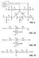
- FIGS. 1A and 1B are schematic diagrams of circuits for reducing third order distortion in accordance with the present invention.
- FIG. 2 is a graph of the diode differential forward resistance R F verses the diode forward current I F .
- FIG. 3 is a graph of the diode differential forward resistance R F verses the diode forward current I F with different resistors in series with the diode.
- FIG. 4 is an alternative embodiment of the present invention.
- FIG. 5 is a bias control for the present invention.
- FIG. 6 is a schematic diagram of a circuit for reducing second and third order distortion in accordance with the present invention.
- FIGS. 7A-7C are schematic diagrams of bias control circuits for the distortion circuit of FIG. 6 .
- Nonlinear element One basic structural element for a compensator is a nonlinear element.
- the nonlinear element is preferably a Schottky diode pair.
- Diode current I F and diode voltage U F are generally related by the following equation:
- I F is the diode forward current
- I 0 is the diode inverse current
- U F is the diode forward voltage
- m is a correction factor with a value between 1 and 2
- T temperature in kelvin
- U T is a constant for a certain temperature, (for example, 25 mV at 23° C.).
- the Taylor series of an exponential function yields relatively large second and third order terms. This is expressed in Equation 6 whereby the last term is the third order term and the next-to-last term is the second order term. ⁇ x ⁇ 1 + x ( 1 ! ) + x 2 ( 2 ! ) + x 3 ( 3 ! ) Equation 6
- Equation 4 can be approximated by:
- Equation 6 Assuming that k ⁇ U in is x, and inserting it into Equation 6, the third order term x 3 /3! and the second order term x 2 /2! will produce the same products, (i.e., compensating products generated by the diode), as shown by Equation 1.
- the nonlinear element is connected in accordance with the preferred embodiment of the present invention in the transverse branch of a T-member as shown in FIG. 1 A. If the nonlinear element was arranged in the length branch of an equivalent T-member, the IM products would be in phase relative to those to be compensated, (provided the diodes in the two cases operate at the same operating points), and compensation would be impossible.
- the system 10 for reducing second and third order IM products in accordance with the present invention is located between an input E and an output A.
- the input E comprises a multifrequency operating signal, for example a CATV signal having plurality of CATV channels.
- the output A is connected to a system to be compensated, for example a hybrid RF amplifier, a laser or any other nonlinear quadrapole.
- a system to be compensated for example a hybrid RF amplifier, a laser or any other nonlinear quadrapole.
- the system will be explained hereinafter with reference to the example of being connected to an RF amplifier.
- the RF amplifier not only amplifies the output A, but also may introduce undesired second and third order IM products. These IM products are compensated for by the present invention.
- the system 10 is a circuit which comprises a plurality of resistors R 1 , R 2 , R 3 , R 4 ; a plurality of capacitors C 1 , C 2 , C 3 , C 4 , C 5 , C 6 ; and a nonlinear element comprising two Schottky barrier diodes D 1 , D 2 .
- the present invention produces second and third order “compensating” IM products, (including cross-modulation products), which exhibit the same amplitude but opposite phase to the undesired RF amplifier-generated IM products.
- the compensating IM products are added at the node connecting the two resistors R 3 and R 4 and the two diodes D 1 and D 2 such that the compensating IM products are added to the multifrequency operating signal and output at output A.
- a first control input S 1 is provided to control the operating point of the diodes D 1 , D 2 and thereby control the magnitude of compensating IM products.
- a direct current (DC) is supplied which flows through diodes D 1 and D 2 and determines the operating point of the diodes D 1 , D 2 .
- a DC current change at the control input S 1 influences the steepness of the diode characteristic.
- the change in the diode differential forward resistance R F in the lower segment of the diode characteristic is greater than in the upper segment, provided that the change of I F is the same in both cases.
- FIG. 2 A graph of the diode differential forward resistance R F verses the diode forward current I F is shown in FIG. 2 . It should be noted that this curve is an illustration of the frequency response at 10 KHz. As shown, the diode differential forward resistance R F is dependent upon both the diode operating point and the change in diode forward current I F . For example, the DC current at the first control input S 1 changes the operating point of the diodes D 1 , D 2 from operating point A to operating point B. At operating point A, a change in the diode forward current I F of 0.5 mA results in a change in the diode differential forward resistance R F of 155 ⁇ .
- the magnitude of the compensating IM products is dependent upon the change in diode differential forward resistance R F as a function of the level of U in . Accordingly, a low DC current at the first control input S 1 leads to a greater magnitude of compensating IM products, and a high DC current at the first control input S 1 correspondingly leads to a smaller magnitude of compensating IM products.
- the magnitude of the compensating IM may be selectively controlled.
- separately biasing each diode D 1 , D 2 enables the present invention to selectively control the amount of second and third order distortion that is created.
- an additional method for adjusting the diode differential forward resistance R F characteristic is provided by the introduction of the resistors R 1 and R 2 , which from an AC standpoint are in series with D 1 and D 2 .
- the signal currents are conducted from D 2 via R 2 directly to ground and from D 1 via R 1 and C 6 to ground.
- C 6 is a blocking capacitor whose complex resistance is negligibly small for all applied frequencies of the multifrequency input signal.
- the resistors R 1 and R 2 affect the diode differential forward resistance R F characteristic by flattening the characteristic, thereby influencing the magnitude of the compensating IM products.
- FIG. 3 a graph of the diode differential forward resistance R F verses the diode forward current I F is shown. It can clearly be seen that as the value of the two resistors R 1 , R 2 is increased from 10 ⁇ to 100 ⁇ , the diode differential forward resistance R F characteristic changes from curve C to curve D.
- the resistors R 1 , R 2 have the same values and simultaneously play the role of symmetry resistors, in that they equalize the potentially different diodes D 1 , D 2 .
- the symmetry resistors R 1 and R 2 decouple the two diodes D 1 , D 2 from each other and lead to symmetrical compensating IM products. In this manner, any deviations in the characteristics of both diodes D 1 , D 2 are minimized.
- the bias on each of the diodes D 1 , D 2 is different. Accordingly, for every RF positive cycle and negative cycle, the compensating products generated by D 1 will be different than the compensating products generated by D 2 . In this manner, in addition to providing third order correction, the present circuit will also provide second order correction.
- the diode differential forward resistance R F is frequency dependent due to the complex parasitic effects of the diodes D 1 , D 2 . As the diode current I F decreases, the influence of the parasitic elements increases. The detrimental diffusion capacitance of the diodes D 1 , D 2 , (which parallels the diode differential forward resistance R F ), prevents the signal energy at the upper frequency limit from entering into the diode differential forward resistance R F . This leads to a reduction of the compensating IM products at high frequencies. Unfortunately, a high level of compensating IM products is particularly required at high frequencies because the IM products in RF amplifiers inherently increase with signal frequency due to the circuit-produced reverse coupling, which becomes less effective at high frequencies.
- capacitors C 1 , C 2 and C 3 are provided.
- the common variable capacitor C 3 is used to match the frequency distribution of the IM products of the RF amplifier, thereby achieving optimal broadband compensation.
- the capacitors C 4 and C 5 serve exclusively for blocking the direct components at the input E and output A, and their capacitances are large enough such that they do not affect the multifrequency operating signal.
- the capacitors C 1 , C 2 and C 3 provide frequency-dependent resistances, such that they permit a desired and controllable level of increase of the compensating IM products at high frequencies.
- the flattening of the diode characteristic at high frequencies is counteracted by the reduction of the complex series resistances. As a result, the diode characteristic steepens not only at high frequencies, but an increase in steepness can also be realized if desired.
- an improvement of 8 db to 15 db in CTB and X-mod may be expected depending upon the hybrid RF amplifier to which the system 10 is coupled.
- FIG. 1 B An alternative embodiment 15 of the present invention is shown in FIG. 1 B.
- This embodiment 15 is similar to the embodiment shown in FIG. 1A except that the ground connections have essentially been exchanged with the input and output.
- R11 is part of the first DC control input S 1
- C 7 is a blocking capacitor
- choke 1 is a path only for the DC current from the control input S 1 .
- This embodiment 15 operates in the same manner and achieves the same results as the embodiment 10 shown in FIG. 1 A.
- FIG. 4 Another alternative embodiment 20 of the present invention is shown in FIG. 4 .
- C 3 is replaced by the variable capacitance diode D 3 .
- An input S 2 is provided for connection to a variable DC voltage. This permits electrical adjustments, for example, when the circuit 20 is integrated into a hybrid RF amplifier.
- the value of R 5 is chosen to be very high so that there is no adverse influence to the RF transmission behavior of the distortion system, (i.e., no adverse influence on insertion loss and return loss over the range of operating frequencies).
- the input voltage +U B is the operating voltage which has a fixed value.
- the fixed value is 24 volts DC, which corresponds to the operating voltage of a hybrid RF amplifier.
- the value of +U B may be different in other applications.
- R 12 is a resistor with a positive temperature coefficient to compensate temperature effects. With the insertion of R 12 it is possible to realize temperature compensation of the RF hybrid, (i.e., increased compensation as the temperature increases). It should be noted that although R 12 improves the temperature behavior, this resistor is optional. Since R 13 is variable, it permits adjustment of the compensation effect of the IM products.
- Table 1 below sets forth the component values for the components shown in FIGS. 1, 4 , 5 and 6 . It should be clearly recognized by those skilled in the art that these component values have been selected for the particular application and desired frequency range. These component values are illustrative only and should not be considered to be an essential part of the present invention since they will change depending upon the operating range of the system in which the distortion circuit is utilized and the amplifier to which the distortion circuit is coupled. The values should not be viewed as limiting.
- the preferred embodiment of the present invention comprises anti-parallel connected diode branches D 1 , D 2 whereby the second order products produced in each branch cancel each other out since their individual signals are oppositely phased.
- an asymmetry maybe intentionally created resulting in second order products which appear at the output A of the circuit. The magnitude of these products depends upon the degree of asymmetry and the DC current in the control input S 1 ; whereas the phase 0°/180° depends on the weighting of the components from both diode branches D 1 , D 2 . This assumes that D 1 causes products at 0° and D 2 causes products at 180° (opposite phase).
- a bias control B makes the bias across the diodes D 1 , D 2 different with respect to each other such that diode D 1 produces a different amount of compensating products than diode D 2 .
- three additional inputs S 2 , S 3 and S 4 are provided from the bias control B to control the amount of DC current supplied to the diodes D 1 and D 2 . Controlling the amount of DC current across each of diodes D 1 and D 2 causes diodes D 1 and D 2 to exhibit different operating points, thereby generating second order IM compensating products that sum together.
- the three additional inputs S 2 , S 3 , S 4 are DC current sources, each of which may be selectively controlled and adjusted in order to control the amount of DC current supplied to the diodes D 1 , D 2 .
- DC current sources each of which may be selectively controlled and adjusted in order to control the amount of DC current supplied to the diodes D 1 , D 2 .
- the bias control B is configured such that the sum of the third order products remains substantially constant and that the third order products are further affected only by the control input S 1 .
- the bias control B only effects the generation of second order products.
- the present invention achieves the most independent possible relative adjustment of second and third order products and thereby provides practicable equalization.
- FIGS. 7A-7C several embodiments of DC current inputs S 2 , S 3 , S 4 for use as a bias control circuit B to selectively control the output of DC current are shown in FIGS. 7A-7C.
- FIG. 7A is a DC current input control circuit for input S 3 comprising three resistors R 21 , R 23 , R 24 and a potentiometer R 22 .
- FIG. 7B is a DC current input control circuit for inputs S 2 , S 3 and S 4 comprising resistors R 31 , R 33 and R 34 and potentiometer R 32 . Adjustment of the potentiometer controls the amount of DC current from the inputs S 2 , S 3 , S 4 .
- resistor R 24 can be replaced by choke 2 and resistor R 34 can be replaced by choke 3 to provide a pure DC path.
- FIG. 7C shows a circuit for inputs S 2 and S 4 comprising two capacitors C 41 and C 42 , two resistors R 41 and R 43 and a potentiometer R 42 .
- this circuit by setting the potentiometer R 42 slide to ground, (away from its mid-point setting), an intentional and controlled asymmetry is achieved between the two diodes D 1 , D 2 .
- the resulting resistance components of FIG. 7C are parallel to R 1 and R 2 from an RF standpoint.
- the function of R 1 and R 2 has previously been described hereinbefore.
- Upon deviation from the mid-point setting of the potentiometer R 42 there are created different diode differential forward resistances R F and their accompanying different diode characteristics.
- component R 1 may be changed such that it is different than R 2
- capacitor C 1 may be changed such that it is different than capacitor C 2 .
- This may also be accomplished by connecting additional complex resistances or reactions in parallel with resistance R 1 or resistance R 2 .
- Table 2 below sets forth the component values for the components shown in FIGS. 7A-7C. It should be clearly recognized by those skilled in the art that these component values have been selected for the particular application and desired frequency range. These component values are illustrative only and should not be considered to be an essential part of the present invention since they will change depending upon the operating range of the system in which the distortion circuit is utilized and the amplifier to which the distortion circuit is coupled. The values should not be viewed as limiting.
- circuits described herein and shown in the figures are for a positive supply voltage, and that all circuits can also be configured for negative or symmetrical positive-negative-supply voltages. Although these circuits would have a different layout, they would function in the same manner and achieve the same results as the circuits described herein.
Abstract
Description


| TABLE 1 | |||
| Component | Value | ||
| C1 | 0.5 pF | ||
| C2 | 0.5 pF | ||
| C3 | 0.5-2 pF | ||
| C4, C5, C6, |
1 nF | ||
| R1, R2 | 300 Ω to 750 Ω (dependent on application) | ||
| R3, R4 | 3.9 | ||
| R | |||
| 5 | 10 kΩ-100 kΩ | ||
| D1, D2 | Schottky barrier diode pair | ||
| D3 | Hyperabrupt variable capacitance diode from | ||
| 0.5-2.0 pF | |||
| S1 bias current | 0.8 mA to 2 mA | ||
| R11 | 7.5 kΩ | ||
| |
2 kΩ | ||
| R13 | 20 kΩ | ||
| R14 | 7.5 | ||
| choke | |||
| 1 | 1000 nH | ||
| TABLE 2 | |||
| Component | Value | ||
| R21, R23, R31, R33 | 300 Ω | ||
| R24, |
1 kΩ | ||
| R41, R43 | 270 Ω | ||
| R42 | 500 Ω | ||
| C41, |
1 nF | ||
| choke2, choke3 | 1000 nH | ||
Claims (9)
Priority Applications (1)
| Application Number | Priority Date | Filing Date | Title |
|---|---|---|---|
| US10/303,611 US6759897B2 (en) | 2000-01-24 | 2002-11-25 | Circuit for reducing second and third order intermodulation distortion for a broadband RF amplifier |
Applications Claiming Priority (3)
| Application Number | Priority Date | Filing Date | Title |
|---|---|---|---|
| US09/489,625 US6466084B1 (en) | 2000-01-24 | 2000-01-24 | Circuit for reducing third order intermodulation distortion for a broadband RF amplifier |
| US09/617,610 US6509789B1 (en) | 2000-01-24 | 2000-07-17 | Circuit for reducing second and third order intermodulation distortion for a broadband RF amplifier |
| US10/303,611 US6759897B2 (en) | 2000-01-24 | 2002-11-25 | Circuit for reducing second and third order intermodulation distortion for a broadband RF amplifier |
Related Parent Applications (1)
| Application Number | Title | Priority Date | Filing Date |
|---|---|---|---|
| US09/617,610 Continuation US6509789B1 (en) | 2000-01-24 | 2000-07-17 | Circuit for reducing second and third order intermodulation distortion for a broadband RF amplifier |
Publications (2)
| Publication Number | Publication Date |
|---|---|
| US20030080808A1 US20030080808A1 (en) | 2003-05-01 |
| US6759897B2 true US6759897B2 (en) | 2004-07-06 |
Family
ID=27049769
Family Applications (2)
| Application Number | Title | Priority Date | Filing Date |
|---|---|---|---|
| US09/617,610 Expired - Fee Related US6509789B1 (en) | 2000-01-24 | 2000-07-17 | Circuit for reducing second and third order intermodulation distortion for a broadband RF amplifier |
| US10/303,611 Expired - Lifetime US6759897B2 (en) | 2000-01-24 | 2002-11-25 | Circuit for reducing second and third order intermodulation distortion for a broadband RF amplifier |
Family Applications Before (1)
| Application Number | Title | Priority Date | Filing Date |
|---|---|---|---|
| US09/617,610 Expired - Fee Related US6509789B1 (en) | 2000-01-24 | 2000-07-17 | Circuit for reducing second and third order intermodulation distortion for a broadband RF amplifier |
Country Status (10)
| Country | Link |
|---|---|
| US (2) | US6509789B1 (en) |
| EP (1) | EP1254507B1 (en) |
| AT (1) | ATE254356T1 (en) |
| AU (1) | AU2001231074A1 (en) |
| DE (1) | DE60101212T2 (en) |
| DK (1) | DK1254507T3 (en) |
| ES (1) | ES2210123T3 (en) |
| PT (1) | PT1254507E (en) |
| TW (1) | TW511328B (en) |
| WO (1) | WO2001054268A2 (en) |
Cited By (7)
| Publication number | Priority date | Publication date | Assignee | Title |
|---|---|---|---|---|
| US20060203863A1 (en) * | 2005-03-07 | 2006-09-14 | Shigeo Hayashi | Optical transmitter with a least pair of semiconductor laser diodes |
| US20090041474A1 (en) * | 2007-08-07 | 2009-02-12 | Applied Optoelectronics, Inc. | Predistortion circuit including distortion generator diodes with adjustable diode bias |
| US20090196630A1 (en) * | 2008-02-05 | 2009-08-06 | Applied Optoelectronics, Inc. | Distortion Compensation Circuit Including One or More Phase Invertible Distortion Paths |
| US20090196629A1 (en) * | 2008-02-05 | 2009-08-06 | Applied Optoelectronics, Inc. | Distortion compensation circuit and method based on orders of time dependent series of distortion signal |
| US20130120218A1 (en) * | 2011-11-11 | 2013-05-16 | Yen-Liang Kuo | Multi-Feed Antenna |
| US8606116B2 (en) | 2011-01-13 | 2013-12-10 | Applied Optoelectronics, Inc. | System and method for distortion compensation in response to frequency detection |
| US8891974B2 (en) | 2012-03-30 | 2014-11-18 | Applied Optoelectronics, Inc. | Distortion compensation circuit including tunable phase path |
Families Citing this family (3)
| Publication number | Priority date | Publication date | Assignee | Title |
|---|---|---|---|---|
| US7208992B1 (en) * | 2001-11-08 | 2007-04-24 | C-Cor.Net Corporation | Lossy linearizers for analog optical transmitters |
| US7634198B2 (en) * | 2006-06-21 | 2009-12-15 | Emcore Corporation | In-line distortion cancellation circuits for linearization of electronic and optical signals with phase and frequency adjustment |
| US10574190B2 (en) | 2015-05-06 | 2020-02-25 | Skyworks Solutions, Inc. | RF power amplifiers with diode linearizer |
Citations (36)
| Publication number | Priority date | Publication date | Assignee | Title |
|---|---|---|---|---|
| GB1381597A (en) | 1971-07-22 | 1975-01-22 | Marconi Co Ltd | High frequency amplifier arrangements |
| DE2656436A1 (en) | 1976-12-14 | 1978-06-15 | Licentia Gmbh | Amplifier with inter-modulation compensation - has two directional couplers with second amplifier and phase and amplitude matching elements to compensate inter-modulation |
| DE3024533A1 (en) | 1980-06-28 | 1982-01-21 | Robert Bosch Gmbh, 7000 Stuttgart | Compensating circuit for intermodulation interference of VHF signal - interference signal being filtered out by anti-parallel diodes and inverted, esp. for third order interference |
| DE3338024A1 (en) | 1983-10-20 | 1985-05-02 | Standard Elektrik Lorenz Ag, 7000 Stuttgart | AMPLIFIER WITH CURRENT-VOLTAGE CONVERSION, IN PARTICULAR PRE-AMPLIFIER OF AN OPTICAL RECEIVER |
| GB2164515A (en) | 1984-09-13 | 1986-03-19 | American Telephone & Telegraph | Improvements in or relating to optical receivers |
| US4808810A (en) | 1986-09-24 | 1989-02-28 | At&T And Philips Telecommunications B.V. | Preamplifier for an optical receiver |
| US4882482A (en) | 1988-10-26 | 1989-11-21 | Tektronix, Inc. | Thermally stabilized optical preamplifier |
| US4992754A (en) | 1989-09-07 | 1991-02-12 | Ortel Corporation | Predistorter for linearization of electronic and optical signals |
| US4998012A (en) | 1989-12-01 | 1991-03-05 | Scientific Atlanta, Inc. | Fiber optic transimpedance receiver |
| EP0486953A2 (en) | 1990-11-21 | 1992-05-27 | Gte Laboratories Incorporated | Second-order predistortion circuit for use with laser diode |
| EP0498456A1 (en) | 1991-02-08 | 1992-08-12 | Ortel Corporation | Predistorter and method for linearization of electronic and optical signals |
| US5161044A (en) | 1989-07-11 | 1992-11-03 | Harmonic Lightwaves, Inc. | Optical transmitters linearized by means of parametric feedback |
| US5172068A (en) | 1990-09-17 | 1992-12-15 | Amoco Corporation | Third-order predistortion linearization circuit |
| EP0552316A1 (en) | 1991-06-18 | 1993-07-28 | FUBA Communications Systems GmbH | Circuit for reducing intermodulation on the use of semiconductor lasers for optical information transmission |
| DE4212772A1 (en) | 1992-04-16 | 1993-10-21 | Bosch Gmbh Robert | Wide-band pre-distortion circuit - compensates for second order distortion in analogue CATV laser diodes over wide frequency range |
| US5321710A (en) | 1993-04-19 | 1994-06-14 | Raynet Corporation | Predistortion method and apparatus for laser linearization |
| EP0620661A1 (en) | 1993-04-14 | 1994-10-19 | Sumitomo Electric Industries, Limited | Distortion generating circuit |
| US5361156A (en) | 1991-12-09 | 1994-11-01 | Scientific-Atlanta, Inc. | Method and apparatus for predistortion |
| US5418637A (en) | 1992-10-21 | 1995-05-23 | At&T Corp. | Cascaded distortion compensation for analog optical systems |
| US5424680A (en) | 1993-11-30 | 1995-06-13 | Harmonic Lightwaves, Inc. | Predistorter for high frequency optical communications devices |
| US5455705A (en) | 1994-03-14 | 1995-10-03 | Analog Devices, Inc. | Transimpedance amplifier for optical receiver |
| US5523716A (en) | 1994-10-13 | 1996-06-04 | Hughes Aircraft Company | Microwave predistortion linearizer |
| US5568087A (en) | 1994-06-13 | 1996-10-22 | Agence Spatiale Europeenne | Pre-distorting linearization circuit |
| US5572161A (en) | 1995-06-30 | 1996-11-05 | Harris Corporation | Temperature insensitive filter tuning network and method |
| US5589797A (en) | 1995-09-26 | 1996-12-31 | Lucent Technologies Inc. | Low distortion amplifier |
| WO1997035390A1 (en) | 1996-03-20 | 1997-09-25 | Philips Electronics N.V. | Predistortion circuit for an analog signal in a video communication network |
| US5703530A (en) | 1995-10-06 | 1997-12-30 | Yagi Antenna Co., Ltd. | Radio frequency amplifier having improved CTB and cross modulation characteristics |
| US5752174A (en) | 1993-07-31 | 1998-05-12 | Nec Corporation | Radio receiver with automatic adjustment of oscillation frequencies |
| US5798854A (en) | 1994-05-19 | 1998-08-25 | Ortel Corporation | In-line predistorter for linearization of electronic and optical signals |
| US5850305A (en) | 1996-12-18 | 1998-12-15 | Scientific-Atlanta, Inc. | Adaptive predistortion control for optical external modulation |
| US5909642A (en) | 1996-07-05 | 1999-06-01 | Fujitsu Limited | Nonlinear distortion detecting circuit and nonlinear distortion compensating circuit for transmitter |
| US5939920A (en) * | 1996-03-08 | 1999-08-17 | Fujitsu Limited | Method and apparatus which adds distortion to a signal to compensate for distortion added at a later stage by a nonlinear element |
| US6069534A (en) | 1997-12-04 | 2000-05-30 | Trw Inc. | Balance photo-receiver with complementary HBT common-base push pull pre-amplifier |
| US6107877A (en) | 1999-04-09 | 2000-08-22 | General Instrument Corporation | Predistortion generator coupled with an RF amplifier |
| US6122085A (en) | 1997-04-08 | 2000-09-19 | Lucent Technologies Inc. | Lightwave transmission techniques |
| US6204718B1 (en) | 1999-06-25 | 2001-03-20 | Scientific-Atlanta, Inc. | Method and apparatus for generating second-order predistortion without third-order distortion |
Family Cites Families (1)
| Publication number | Priority date | Publication date | Assignee | Title |
|---|---|---|---|---|
| US5481389A (en) * | 1992-10-09 | 1996-01-02 | Scientific-Atlanta, Inc. | Postdistortion circuit for reducing distortion in an optical communications system |
-
2000
- 2000-07-17 US US09/617,610 patent/US6509789B1/en not_active Expired - Fee Related
-
2001
- 2001-01-20 TW TW090101417A patent/TW511328B/en not_active IP Right Cessation
- 2001-01-23 WO PCT/US2001/002155 patent/WO2001054268A2/en active IP Right Grant
- 2001-01-23 AU AU2001231074A patent/AU2001231074A1/en not_active Abandoned
- 2001-01-23 AT AT01903229T patent/ATE254356T1/en not_active IP Right Cessation
- 2001-01-23 DE DE60101212T patent/DE60101212T2/en not_active Expired - Fee Related
- 2001-01-23 PT PT01903229T patent/PT1254507E/en unknown
- 2001-01-23 DK DK01903229T patent/DK1254507T3/en active
- 2001-01-23 EP EP01903229A patent/EP1254507B1/en not_active Expired - Lifetime
- 2001-01-23 ES ES01903229T patent/ES2210123T3/en not_active Expired - Lifetime
-
2002
- 2002-11-25 US US10/303,611 patent/US6759897B2/en not_active Expired - Lifetime
Patent Citations (38)
| Publication number | Priority date | Publication date | Assignee | Title |
|---|---|---|---|---|
| GB1381597A (en) | 1971-07-22 | 1975-01-22 | Marconi Co Ltd | High frequency amplifier arrangements |
| DE2656436A1 (en) | 1976-12-14 | 1978-06-15 | Licentia Gmbh | Amplifier with inter-modulation compensation - has two directional couplers with second amplifier and phase and amplitude matching elements to compensate inter-modulation |
| DE3024533A1 (en) | 1980-06-28 | 1982-01-21 | Robert Bosch Gmbh, 7000 Stuttgart | Compensating circuit for intermodulation interference of VHF signal - interference signal being filtered out by anti-parallel diodes and inverted, esp. for third order interference |
| DE3338024A1 (en) | 1983-10-20 | 1985-05-02 | Standard Elektrik Lorenz Ag, 7000 Stuttgart | AMPLIFIER WITH CURRENT-VOLTAGE CONVERSION, IN PARTICULAR PRE-AMPLIFIER OF AN OPTICAL RECEIVER |
| GB2164515A (en) | 1984-09-13 | 1986-03-19 | American Telephone & Telegraph | Improvements in or relating to optical receivers |
| US4808810A (en) | 1986-09-24 | 1989-02-28 | At&T And Philips Telecommunications B.V. | Preamplifier for an optical receiver |
| US4882482A (en) | 1988-10-26 | 1989-11-21 | Tektronix, Inc. | Thermally stabilized optical preamplifier |
| US5161044A (en) | 1989-07-11 | 1992-11-03 | Harmonic Lightwaves, Inc. | Optical transmitters linearized by means of parametric feedback |
| US4992754A (en) | 1989-09-07 | 1991-02-12 | Ortel Corporation | Predistorter for linearization of electronic and optical signals |
| US4992754B1 (en) | 1989-09-07 | 1997-10-28 | Ortel Corp | Predistorter for linearization of electronic and optical signals |
| US4998012A (en) | 1989-12-01 | 1991-03-05 | Scientific Atlanta, Inc. | Fiber optic transimpedance receiver |
| US5172068A (en) | 1990-09-17 | 1992-12-15 | Amoco Corporation | Third-order predistortion linearization circuit |
| EP0486953A2 (en) | 1990-11-21 | 1992-05-27 | Gte Laboratories Incorporated | Second-order predistortion circuit for use with laser diode |
| EP0498456A1 (en) | 1991-02-08 | 1992-08-12 | Ortel Corporation | Predistorter and method for linearization of electronic and optical signals |
| EP0552316A1 (en) | 1991-06-18 | 1993-07-28 | FUBA Communications Systems GmbH | Circuit for reducing intermodulation on the use of semiconductor lasers for optical information transmission |
| US5361156A (en) | 1991-12-09 | 1994-11-01 | Scientific-Atlanta, Inc. | Method and apparatus for predistortion |
| DE4212772A1 (en) | 1992-04-16 | 1993-10-21 | Bosch Gmbh Robert | Wide-band pre-distortion circuit - compensates for second order distortion in analogue CATV laser diodes over wide frequency range |
| US5418637A (en) | 1992-10-21 | 1995-05-23 | At&T Corp. | Cascaded distortion compensation for analog optical systems |
| US5600472A (en) | 1993-04-14 | 1997-02-04 | Sumitomo Electric Industries, Ltd. | Distortion generating circuit |
| EP0620661A1 (en) | 1993-04-14 | 1994-10-19 | Sumitomo Electric Industries, Limited | Distortion generating circuit |
| US5321710A (en) | 1993-04-19 | 1994-06-14 | Raynet Corporation | Predistortion method and apparatus for laser linearization |
| US5752174A (en) | 1993-07-31 | 1998-05-12 | Nec Corporation | Radio receiver with automatic adjustment of oscillation frequencies |
| US5424680A (en) | 1993-11-30 | 1995-06-13 | Harmonic Lightwaves, Inc. | Predistorter for high frequency optical communications devices |
| US5455705A (en) | 1994-03-14 | 1995-10-03 | Analog Devices, Inc. | Transimpedance amplifier for optical receiver |
| US5798854A (en) | 1994-05-19 | 1998-08-25 | Ortel Corporation | In-line predistorter for linearization of electronic and optical signals |
| US5568087A (en) | 1994-06-13 | 1996-10-22 | Agence Spatiale Europeenne | Pre-distorting linearization circuit |
| US5523716A (en) | 1994-10-13 | 1996-06-04 | Hughes Aircraft Company | Microwave predistortion linearizer |
| US5572161A (en) | 1995-06-30 | 1996-11-05 | Harris Corporation | Temperature insensitive filter tuning network and method |
| US5589797A (en) | 1995-09-26 | 1996-12-31 | Lucent Technologies Inc. | Low distortion amplifier |
| US5703530A (en) | 1995-10-06 | 1997-12-30 | Yagi Antenna Co., Ltd. | Radio frequency amplifier having improved CTB and cross modulation characteristics |
| US5939920A (en) * | 1996-03-08 | 1999-08-17 | Fujitsu Limited | Method and apparatus which adds distortion to a signal to compensate for distortion added at a later stage by a nonlinear element |
| WO1997035390A1 (en) | 1996-03-20 | 1997-09-25 | Philips Electronics N.V. | Predistortion circuit for an analog signal in a video communication network |
| US5909642A (en) | 1996-07-05 | 1999-06-01 | Fujitsu Limited | Nonlinear distortion detecting circuit and nonlinear distortion compensating circuit for transmitter |
| US5850305A (en) | 1996-12-18 | 1998-12-15 | Scientific-Atlanta, Inc. | Adaptive predistortion control for optical external modulation |
| US6122085A (en) | 1997-04-08 | 2000-09-19 | Lucent Technologies Inc. | Lightwave transmission techniques |
| US6069534A (en) | 1997-12-04 | 2000-05-30 | Trw Inc. | Balance photo-receiver with complementary HBT common-base push pull pre-amplifier |
| US6107877A (en) | 1999-04-09 | 2000-08-22 | General Instrument Corporation | Predistortion generator coupled with an RF amplifier |
| US6204718B1 (en) | 1999-06-25 | 2001-03-20 | Scientific-Atlanta, Inc. | Method and apparatus for generating second-order predistortion without third-order distortion |
Non-Patent Citations (9)
| Title |
|---|
| Bertelsmeier et al., Linearization of Broadband Optical Transmission Systems by Adaptive Predistortion, 1984, pp. 206-212. |
| Eggers, 2GHz Bandwidth Predistortion Linearizer For Microwave Power Amplifiers At Ku-Band, pp. 1501-1505, Sep. 1994. |
| Eggers, Pamela-Linearized Solid State Power Amplifier At Ku-band Frequency, pp. 443-445, Sep. 1993. |
| Ha, Solid-State Microwave Amplifier Design, pp. 202-217. |
| Khilla et al., Semiconductor Transmitter Amplifiers And Traveling Wave Tube Linears For Future Communications Satellites, 8273 ANT Telecommunications Engineering Reports, No. 8, Feb. 1991 (including English translation). |
| Kobayashi et al., A Novel Monolithic Linearized HEMT LNA Using HBT Tuneable Active Feedback, IEEE MTT-S International Microwave Symposium Digest, pp. 1217-1220, Jun. 1996. |
| Locatelli et al., Microwave Linear Power Amplifier With Micromodule Technology, pp. 1.3.1-1.3.6, Jun. 1987. |
| Ohr, GaAs Finds Home in Wireless & High-Speed Data-Communications Applications, Computer Design, Mar. 1994, pp. 59-68. |
| Optical Receiver Front-End Nonlinear Distortion, Electronics Letters, Apr. 29, 1982, vol. 18, No. 9, pp. 361-362. |
Cited By (13)
| Publication number | Priority date | Publication date | Assignee | Title |
|---|---|---|---|---|
| US7415053B2 (en) * | 2005-03-07 | 2008-08-19 | Sumitomo Electric Industries, Ltd. | Optical transmitter with a least pair of semiconductor laser diodes |
| US20060203863A1 (en) * | 2005-03-07 | 2006-09-14 | Shigeo Hayashi | Optical transmitter with a least pair of semiconductor laser diodes |
| US7925170B2 (en) | 2007-08-07 | 2011-04-12 | Applied Optoelectronics, Inc. | Predistortion circuit including distortion generator diodes with adjustable diode bias |
| US20090041474A1 (en) * | 2007-08-07 | 2009-02-12 | Applied Optoelectronics, Inc. | Predistortion circuit including distortion generator diodes with adjustable diode bias |
| US8073340B2 (en) | 2008-02-05 | 2011-12-06 | Applied Optoelectronics, Inc. | Distortion compensation circuit including one or more phase invertible distortion paths |
| US20090196629A1 (en) * | 2008-02-05 | 2009-08-06 | Applied Optoelectronics, Inc. | Distortion compensation circuit and method based on orders of time dependent series of distortion signal |
| US20090196630A1 (en) * | 2008-02-05 | 2009-08-06 | Applied Optoelectronics, Inc. | Distortion Compensation Circuit Including One or More Phase Invertible Distortion Paths |
| US8121493B2 (en) | 2008-02-05 | 2012-02-21 | Applied Optoelectronics, Inc. | Distortion compensation circuit and method based on orders of time dependent series of distortion signal |
| US8718489B2 (en) | 2008-02-05 | 2014-05-06 | Applied Optoelectronics, Inc. | Distortion compensation circuit including one or more phase invertible distortion paths |
| US8606116B2 (en) | 2011-01-13 | 2013-12-10 | Applied Optoelectronics, Inc. | System and method for distortion compensation in response to frequency detection |
| US20130120218A1 (en) * | 2011-11-11 | 2013-05-16 | Yen-Liang Kuo | Multi-Feed Antenna |
| US8988306B2 (en) * | 2011-11-11 | 2015-03-24 | Htc Corporation | Multi-feed antenna |
| US8891974B2 (en) | 2012-03-30 | 2014-11-18 | Applied Optoelectronics, Inc. | Distortion compensation circuit including tunable phase path |
Also Published As
| Publication number | Publication date |
|---|---|
| WO2001054268A2 (en) | 2001-07-26 |
| US20030080808A1 (en) | 2003-05-01 |
| EP1254507B1 (en) | 2003-11-12 |
| DE60101212D1 (en) | 2003-12-18 |
| ES2210123T3 (en) | 2004-07-01 |
| WO2001054268A3 (en) | 2002-02-07 |
| ATE254356T1 (en) | 2003-11-15 |
| PT1254507E (en) | 2004-03-31 |
| DE60101212T2 (en) | 2004-09-09 |
| AU2001231074A1 (en) | 2001-07-31 |
| TW511328B (en) | 2002-11-21 |
| DK1254507T3 (en) | 2004-03-22 |
| US6509789B1 (en) | 2003-01-21 |
| EP1254507A2 (en) | 2002-11-06 |
Similar Documents
| Publication | Publication Date | Title |
|---|---|---|
| US5321710A (en) | Predistortion method and apparatus for laser linearization | |
| AU759069B2 (en) | In-line, unbalanced amplifier, pre-distortion circuit | |
| AU674176B2 (en) | Postdistortion circuit for reducing distortion in an optical communications system | |
| EP1166435B1 (en) | Non-linear distortion generator | |
| EP1794879B1 (en) | Tunable predistorter | |
| US4564816A (en) | Predistortion circuit | |
| US7274257B2 (en) | Variable gain wideband amplifier | |
| US6570430B1 (en) | Non-linear distortion generator for both second and third order distortion | |
| US6759897B2 (en) | Circuit for reducing second and third order intermodulation distortion for a broadband RF amplifier | |
| JPS6386603A (en) | Linearlzer for travelling-wave tube amplifier | |
| US6985020B2 (en) | Inline predistortion for both CSO and CTB correction | |
| US6466084B1 (en) | Circuit for reducing third order intermodulation distortion for a broadband RF amplifier | |
| JP2002064340A (en) | High frequency power amplifier | |
| US7332971B2 (en) | Multi-gigabit/s transimpedance amplifier for optical networks | |
| US6580319B1 (en) | Amplitude and phase transfer linearization method and apparatus for a wideband amplifier | |
| US8547174B1 (en) | Broadband linearizer with combined second and third order generation with adjustable tilt |
Legal Events
| Date | Code | Title | Description |
|---|---|---|---|
| STCF | Information on status: patent grant |
Free format text: PATENTED CASE |
|
| FPAY | Fee payment |
Year of fee payment: 4 |
|
| FPAY | Fee payment |
Year of fee payment: 8 |
|
| AS | Assignment |
Owner name: BANK OF AMERICA, N.A., AS ADMINISTRATIVE AGENT, IL Free format text: SECURITY AGREEMENT;ASSIGNORS:ARRIS GROUP, INC.;ARRIS ENTERPRISES, INC.;ARRIS SOLUTIONS, INC.;AND OTHERS;REEL/FRAME:030498/0023 Effective date: 20130417 Owner name: BANK OF AMERICA, N.A., AS ADMINISTRATIVE AGENT, ILLINOIS Free format text: SECURITY AGREEMENT;ASSIGNORS:ARRIS GROUP, INC.;ARRIS ENTERPRISES, INC.;ARRIS SOLUTIONS, INC.;AND OTHERS;REEL/FRAME:030498/0023 Effective date: 20130417 |
|
| AS | Assignment |
Owner name: ARRIS TECHNOLOGY, INC., GEORGIA Free format text: MERGER AND CHANGE OF NAME;ASSIGNOR:GENERAL INSTRUMENT CORPORATION;REEL/FRAME:035176/0620 Effective date: 20150101 Owner name: ARRIS TECHNOLOGY, INC., GEORGIA Free format text: MERGER AND CHANGE OF NAME;ASSIGNORS:GENERAL INSTRUMENT CORPORATION;GENERAL INSTRUMENT CORPORATION;REEL/FRAME:035176/0620 Effective date: 20150101 |
|
| AS | Assignment |
Owner name: ARRIS ENTERPRISES, INC., GEORGIA Free format text: ASSIGNMENT OF ASSIGNORS INTEREST;ASSIGNOR:ARRIS TECHNOLOGY, INC;REEL/FRAME:037328/0341 Effective date: 20151214 |
|
| FPAY | Fee payment |
Year of fee payment: 12 |
|
| AS | Assignment |
Owner name: ARRIS ENTERPRISES, INC., PENNSYLVANIA Free format text: TERMINATION AND RELEASE OF SECURITY INTEREST IN PATENTS;ASSIGNOR:BANK OF AMERICA, N.A., AS ADMINISTRATIVE AGENT;REEL/FRAME:048825/0294 Effective date: 20190404 Owner name: POWER GUARD, INC., PENNSYLVANIA Free format text: TERMINATION AND RELEASE OF SECURITY INTEREST IN PATENTS;ASSIGNOR:BANK OF AMERICA, N.A., AS ADMINISTRATIVE AGENT;REEL/FRAME:048825/0294 Effective date: 20190404 Owner name: BIG BAND NETWORKS, INC., PENNSYLVANIA Free format text: TERMINATION AND RELEASE OF SECURITY INTEREST IN PATENTS;ASSIGNOR:BANK OF AMERICA, N.A., AS ADMINISTRATIVE AGENT;REEL/FRAME:048825/0294 Effective date: 20190404 Owner name: TEXSCAN CORPORATION, PENNSYLVANIA Free format text: TERMINATION AND RELEASE OF SECURITY INTEREST IN PATENTS;ASSIGNOR:BANK OF AMERICA, N.A., AS ADMINISTRATIVE AGENT;REEL/FRAME:048825/0294 Effective date: 20190404 Owner name: GIC INTERNATIONAL CAPITAL LLC, PENNSYLVANIA Free format text: TERMINATION AND RELEASE OF SECURITY INTEREST IN PATENTS;ASSIGNOR:BANK OF AMERICA, N.A., AS ADMINISTRATIVE AGENT;REEL/FRAME:048825/0294 Effective date: 20190404 Owner name: GENERAL INSTRUMENT CORPORATION, PENNSYLVANIA Free format text: TERMINATION AND RELEASE OF SECURITY INTEREST IN PATENTS;ASSIGNOR:BANK OF AMERICA, N.A., AS ADMINISTRATIVE AGENT;REEL/FRAME:048825/0294 Effective date: 20190404 Owner name: SUNUP DESIGN SYSTEMS, INC., PENNSYLVANIA Free format text: TERMINATION AND RELEASE OF SECURITY INTEREST IN PATENTS;ASSIGNOR:BANK OF AMERICA, N.A., AS ADMINISTRATIVE AGENT;REEL/FRAME:048825/0294 Effective date: 20190404 Owner name: AEROCAST, INC., PENNSYLVANIA Free format text: TERMINATION AND RELEASE OF SECURITY INTEREST IN PATENTS;ASSIGNOR:BANK OF AMERICA, N.A., AS ADMINISTRATIVE AGENT;REEL/FRAME:048825/0294 Effective date: 20190404 Owner name: MODULUS VIDEO, INC., PENNSYLVANIA Free format text: TERMINATION AND RELEASE OF SECURITY INTEREST IN PATENTS;ASSIGNOR:BANK OF AMERICA, N.A., AS ADMINISTRATIVE AGENT;REEL/FRAME:048825/0294 Effective date: 20190404 Owner name: LEAPSTONE SYSTEMS, INC., PENNSYLVANIA Free format text: TERMINATION AND RELEASE OF SECURITY INTEREST IN PATENTS;ASSIGNOR:BANK OF AMERICA, N.A., AS ADMINISTRATIVE AGENT;REEL/FRAME:048825/0294 Effective date: 20190404 Owner name: ARRIS SOLUTIONS, INC., PENNSYLVANIA Free format text: TERMINATION AND RELEASE OF SECURITY INTEREST IN PATENTS;ASSIGNOR:BANK OF AMERICA, N.A., AS ADMINISTRATIVE AGENT;REEL/FRAME:048825/0294 Effective date: 20190404 Owner name: THE GI REALTY TRUST 1996, PENNSYLVANIA Free format text: TERMINATION AND RELEASE OF SECURITY INTEREST IN PATENTS;ASSIGNOR:BANK OF AMERICA, N.A., AS ADMINISTRATIVE AGENT;REEL/FRAME:048825/0294 Effective date: 20190404 Owner name: MOTOROLA WIRELINE NETWORKS, INC., PENNSYLVANIA Free format text: TERMINATION AND RELEASE OF SECURITY INTEREST IN PATENTS;ASSIGNOR:BANK OF AMERICA, N.A., AS ADMINISTRATIVE AGENT;REEL/FRAME:048825/0294 Effective date: 20190404 Owner name: NETOPIA, INC., PENNSYLVANIA Free format text: TERMINATION AND RELEASE OF SECURITY INTEREST IN PATENTS;ASSIGNOR:BANK OF AMERICA, N.A., AS ADMINISTRATIVE AGENT;REEL/FRAME:048825/0294 Effective date: 20190404 Owner name: QUANTUM BRIDGE COMMUNICATIONS, INC., PENNSYLVANIA Free format text: TERMINATION AND RELEASE OF SECURITY INTEREST IN PATENTS;ASSIGNOR:BANK OF AMERICA, N.A., AS ADMINISTRATIVE AGENT;REEL/FRAME:048825/0294 Effective date: 20190404 Owner name: ACADIA AIC, INC., PENNSYLVANIA Free format text: TERMINATION AND RELEASE OF SECURITY INTEREST IN PATENTS;ASSIGNOR:BANK OF AMERICA, N.A., AS ADMINISTRATIVE AGENT;REEL/FRAME:048825/0294 Effective date: 20190404 Owner name: BROADBUS TECHNOLOGIES, INC., PENNSYLVANIA Free format text: TERMINATION AND RELEASE OF SECURITY INTEREST IN PATENTS;ASSIGNOR:BANK OF AMERICA, N.A., AS ADMINISTRATIVE AGENT;REEL/FRAME:048825/0294 Effective date: 20190404 Owner name: ARRIS HOLDINGS CORP. OF ILLINOIS, INC., PENNSYLVAN Free format text: TERMINATION AND RELEASE OF SECURITY INTEREST IN PATENTS;ASSIGNOR:BANK OF AMERICA, N.A., AS ADMINISTRATIVE AGENT;REEL/FRAME:048825/0294 Effective date: 20190404 Owner name: GIC INTERNATIONAL HOLDCO LLC, PENNSYLVANIA Free format text: TERMINATION AND RELEASE OF SECURITY INTEREST IN PATENTS;ASSIGNOR:BANK OF AMERICA, N.A., AS ADMINISTRATIVE AGENT;REEL/FRAME:048825/0294 Effective date: 20190404 Owner name: NEXTLEVEL SYSTEMS (PUERTO RICO), INC., PENNSYLVANI Free format text: TERMINATION AND RELEASE OF SECURITY INTEREST IN PATENTS;ASSIGNOR:BANK OF AMERICA, N.A., AS ADMINISTRATIVE AGENT;REEL/FRAME:048825/0294 Effective date: 20190404 Owner name: GENERAL INSTRUMENT INTERNATIONAL HOLDINGS, INC., P Free format text: TERMINATION AND RELEASE OF SECURITY INTEREST IN PATENTS;ASSIGNOR:BANK OF AMERICA, N.A., AS ADMINISTRATIVE AGENT;REEL/FRAME:048825/0294 Effective date: 20190404 Owner name: CCE SOFTWARE LLC, PENNSYLVANIA Free format text: TERMINATION AND RELEASE OF SECURITY INTEREST IN PATENTS;ASSIGNOR:BANK OF AMERICA, N.A., AS ADMINISTRATIVE AGENT;REEL/FRAME:048825/0294 Effective date: 20190404 Owner name: JERROLD DC RADIO, INC., PENNSYLVANIA Free format text: TERMINATION AND RELEASE OF SECURITY INTEREST IN PATENTS;ASSIGNOR:BANK OF AMERICA, N.A., AS ADMINISTRATIVE AGENT;REEL/FRAME:048825/0294 Effective date: 20190404 Owner name: 4HOME, INC., PENNSYLVANIA Free format text: TERMINATION AND RELEASE OF SECURITY INTEREST IN PATENTS;ASSIGNOR:BANK OF AMERICA, N.A., AS ADMINISTRATIVE AGENT;REEL/FRAME:048825/0294 Effective date: 20190404 Owner name: UCENTRIC SYSTEMS, INC., PENNSYLVANIA Free format text: TERMINATION AND RELEASE OF SECURITY INTEREST IN PATENTS;ASSIGNOR:BANK OF AMERICA, N.A., AS ADMINISTRATIVE AGENT;REEL/FRAME:048825/0294 Effective date: 20190404 Owner name: ARRIS KOREA, INC., PENNSYLVANIA Free format text: TERMINATION AND RELEASE OF SECURITY INTEREST IN PATENTS;ASSIGNOR:BANK OF AMERICA, N.A., AS ADMINISTRATIVE AGENT;REEL/FRAME:048825/0294 Effective date: 20190404 Owner name: SETJAM, INC., PENNSYLVANIA Free format text: TERMINATION AND RELEASE OF SECURITY INTEREST IN PATENTS;ASSIGNOR:BANK OF AMERICA, N.A., AS ADMINISTRATIVE AGENT;REEL/FRAME:048825/0294 Effective date: 20190404 Owner name: ARRIS GROUP, INC., PENNSYLVANIA Free format text: TERMINATION AND RELEASE OF SECURITY INTEREST IN PATENTS;ASSIGNOR:BANK OF AMERICA, N.A., AS ADMINISTRATIVE AGENT;REEL/FRAME:048825/0294 Effective date: 20190404 Owner name: GENERAL INSTRUMENT AUTHORIZATION SERVICES, INC., P Free format text: TERMINATION AND RELEASE OF SECURITY INTEREST IN PATENTS;ASSIGNOR:BANK OF AMERICA, N.A., AS ADMINISTRATIVE AGENT;REEL/FRAME:048825/0294 Effective date: 20190404 Owner name: IMEDIA CORPORATION, PENNSYLVANIA Free format text: TERMINATION AND RELEASE OF SECURITY INTEREST IN PATENTS;ASSIGNOR:BANK OF AMERICA, N.A., AS ADMINISTRATIVE AGENT;REEL/FRAME:048825/0294 Effective date: 20190404 Owner name: ARRIS HOLDINGS CORP. OF ILLINOIS, INC., PENNSYLVANIA Free format text: TERMINATION AND RELEASE OF SECURITY INTEREST IN PATENTS;ASSIGNOR:BANK OF AMERICA, N.A., AS ADMINISTRATIVE AGENT;REEL/FRAME:048825/0294 Effective date: 20190404 Owner name: NEXTLEVEL SYSTEMS (PUERTO RICO), INC., PENNSYLVANIA Free format text: TERMINATION AND RELEASE OF SECURITY INTEREST IN PATENTS;ASSIGNOR:BANK OF AMERICA, N.A., AS ADMINISTRATIVE AGENT;REEL/FRAME:048825/0294 Effective date: 20190404 Owner name: GENERAL INSTRUMENT INTERNATIONAL HOLDINGS, INC., PENNSYLVANIA Free format text: TERMINATION AND RELEASE OF SECURITY INTEREST IN PATENTS;ASSIGNOR:BANK OF AMERICA, N.A., AS ADMINISTRATIVE AGENT;REEL/FRAME:048825/0294 Effective date: 20190404 Owner name: GENERAL INSTRUMENT AUTHORIZATION SERVICES, INC., PENNSYLVANIA Free format text: TERMINATION AND RELEASE OF SECURITY INTEREST IN PATENTS;ASSIGNOR:BANK OF AMERICA, N.A., AS ADMINISTRATIVE AGENT;REEL/FRAME:048825/0294 Effective date: 20190404 |
|
| AS | Assignment |
Owner name: ARRIS ENTERPRISES LLC, GEORGIA Free format text: CHANGE OF NAME;ASSIGNOR:ARRIS ENTERPRISES, INC.;REEL/FRAME:049649/0062 Effective date: 20151231 |
|
| AS | Assignment |
Owner name: WILMINGTON TRUST, NATIONAL ASSOCIATION, AS COLLATE Free format text: PATENT SECURITY AGREEMENT;ASSIGNOR:ARRIS ENTERPRISES LLC;REEL/FRAME:049820/0495 Effective date: 20190404 Owner name: JPMORGAN CHASE BANK, N.A., NEW YORK Free format text: TERM LOAN SECURITY AGREEMENT;ASSIGNORS:COMMSCOPE, INC. OF NORTH CAROLINA;COMMSCOPE TECHNOLOGIES LLC;ARRIS ENTERPRISES LLC;AND OTHERS;REEL/FRAME:049905/0504 Effective date: 20190404 Owner name: JPMORGAN CHASE BANK, N.A., NEW YORK Free format text: ABL SECURITY AGREEMENT;ASSIGNORS:COMMSCOPE, INC. OF NORTH CAROLINA;COMMSCOPE TECHNOLOGIES LLC;ARRIS ENTERPRISES LLC;AND OTHERS;REEL/FRAME:049892/0396 Effective date: 20190404 Owner name: WILMINGTON TRUST, NATIONAL ASSOCIATION, AS COLLATERAL AGENT, CONNECTICUT Free format text: PATENT SECURITY AGREEMENT;ASSIGNOR:ARRIS ENTERPRISES LLC;REEL/FRAME:049820/0495 Effective date: 20190404 |
|
| AS | Assignment |
Owner name: ARRIS ENTERPRISES, INC., GEORGIA Free format text: ASSIGNMENT OF ASSIGNORS INTEREST;ASSIGNOR:ARRIS TECHNOLOGY, INC.;REEL/FRAME:060791/0583 Effective date: 20151214 |