US6678446B1 - Multi-band arrayed waveguide grating - Google Patents
Multi-band arrayed waveguide grating Download PDFInfo
- Publication number
- US6678446B1 US6678446B1 US09/970,207 US97020701A US6678446B1 US 6678446 B1 US6678446 B1 US 6678446B1 US 97020701 A US97020701 A US 97020701A US 6678446 B1 US6678446 B1 US 6678446B1
- Authority
- US
- United States
- Prior art keywords
- waveguides
- output
- input
- free propagation
- optical apparatus
- Prior art date
- Legal status (The legal status is an assumption and is not a legal conclusion. Google has not performed a legal analysis and makes no representation as to the accuracy of the status listed.)
- Expired - Lifetime, expires
Links
Images


Classifications
-
- G—PHYSICS
- G02—OPTICS
- G02B—OPTICAL ELEMENTS, SYSTEMS OR APPARATUS
- G02B6/00—Light guides; Structural details of arrangements comprising light guides and other optical elements, e.g. couplings
- G02B6/10—Light guides; Structural details of arrangements comprising light guides and other optical elements, e.g. couplings of the optical waveguide type
- G02B6/12—Light guides; Structural details of arrangements comprising light guides and other optical elements, e.g. couplings of the optical waveguide type of the integrated circuit kind
- G02B6/12007—Light guides; Structural details of arrangements comprising light guides and other optical elements, e.g. couplings of the optical waveguide type of the integrated circuit kind forming wavelength selective elements, e.g. multiplexer, demultiplexer
- G02B6/12009—Light guides; Structural details of arrangements comprising light guides and other optical elements, e.g. couplings of the optical waveguide type of the integrated circuit kind forming wavelength selective elements, e.g. multiplexer, demultiplexer comprising arrayed waveguide grating [AWG] devices, i.e. with a phased array of waveguides
- G02B6/12016—Light guides; Structural details of arrangements comprising light guides and other optical elements, e.g. couplings of the optical waveguide type of the integrated circuit kind forming wavelength selective elements, e.g. multiplexer, demultiplexer comprising arrayed waveguide grating [AWG] devices, i.e. with a phased array of waveguides characterised by the input or output waveguides, e.g. tapered waveguide ends, coupled together pairs of output waveguides
-
- G—PHYSICS
- G02—OPTICS
- G02B—OPTICAL ELEMENTS, SYSTEMS OR APPARATUS
- G02B6/00—Light guides; Structural details of arrangements comprising light guides and other optical elements, e.g. couplings
- G02B6/10—Light guides; Structural details of arrangements comprising light guides and other optical elements, e.g. couplings of the optical waveguide type
- G02B6/12—Light guides; Structural details of arrangements comprising light guides and other optical elements, e.g. couplings of the optical waveguide type of the integrated circuit kind
- G02B6/12007—Light guides; Structural details of arrangements comprising light guides and other optical elements, e.g. couplings of the optical waveguide type of the integrated circuit kind forming wavelength selective elements, e.g. multiplexer, demultiplexer
- G02B6/12009—Light guides; Structural details of arrangements comprising light guides and other optical elements, e.g. couplings of the optical waveguide type of the integrated circuit kind forming wavelength selective elements, e.g. multiplexer, demultiplexer comprising arrayed waveguide grating [AWG] devices, i.e. with a phased array of waveguides
- G02B6/12019—Light guides; Structural details of arrangements comprising light guides and other optical elements, e.g. couplings of the optical waveguide type of the integrated circuit kind forming wavelength selective elements, e.g. multiplexer, demultiplexer comprising arrayed waveguide grating [AWG] devices, i.e. with a phased array of waveguides characterised by the optical interconnection to or from the AWG devices, e.g. integration or coupling with lasers or photodiodes
Definitions
- This invention is in the field of networks for carrying optical signals.
- the invention relates to apparatus for multiplexing or demultiplexing a number of optical bands.
- the invention relates more particularly to such apparatus which incorporates arrayed waveguide gratings.
- Optical fibers provide a way to transmit large volumes of data from place to place. It is often desirable to wavelength multiplex a number of signals onto a single optical fiber. This can be accomplished by passing each signal into a different input of a multiplexer and connecting an output of the multiplexer to the optical fiber. The signals can be recovered at a destination by demultiplexing.
- Arrayed waveguide grating routers are commonly used as multiplexer/demultiplexers in such systems (the same device can typically be used either as a multiplexer, as a demultiplexer, or simultaneously as a multiplexer and a demultiplexer).
- An arrayed waveguide router uses an arrayed waveguide grating to separate signals by wavelength.
- Example AWGRs are described in U.S. Pat. Nos. 5,002,350 and 5,136,671, both invented by Dragone.
- FIG. 1 shows the main functional parts of a simple prior art AWGR 10 .
- AWGR 10 comprises a pair of free propagation regions which are typically implemented as slab waveguides 20 and 30 .
- the free propagation regions are sometimes referred to as “star couplers”.
- a number, M, of input waveguides 22 couple corresponding input ports 26 to input slab waveguide 20 .
- a number, N, of output waveguides 32 couple slab waveguide 30 to a number of corresponding output ports 36 .
- Input waveguides 22 and ports 26 are labeled with the index p with 0 ⁇ p ⁇ 4.
- Output waveguides 32 and ports 36 are labeled with the index q with 0 ⁇ q ⁇ 4.
- the terms “input” and “output” are used herein for reference only. Light can propagate in either direction through AWGR 10 .
- Waveguides 20 and 30 are coupled to one another by a plurality of grating waveguides 16 .
- grating waveguides 16 each have a different length. The lengths of grating waveguides 16 are spaced from one another by predetermined amounts.
- light enters AWGR 10 through at least one of input waveguides 22 and, in sequence, propagates through input slab waveguide 20 , grating waveguides 16 , output slab waveguide 30 , and at least one output waveguide 32 .
- AWGR 10 In the AWGR 10 of FIG. 1, light having a wavelength ⁇ which enters AWGR 10 at a certain one of input waveguides 22 is preferentially coupled into a specific one of output waveguides 32 .
- AWGR 10 has an optical passband associated with each pair of an input port 26 and an output port 36 .
- a port is a location at which a waveguide of AWGR 10 couples to an optical pathway that is external to AWGR 10 .
- a port might be a location at which an input or output waveguide couples to an optical fiber external to the PLC on which the AWGR is fabricated.
- Within each optical passband the optical transmission between input port p and output port q is optimized for a range of wavelengths that are centered at the nominal wavelength for the passband, ⁇ . This can be achieved by designing the AWGR to satisfy the following equation:
- ⁇ is the wavelength
- n s is the effective index of refraction of slab waveguides 20 and 30 ;
- n c is the effective index of refraction of channel waveguides 16 ;
- d I and d o are the center-to-center separations of grating waveguides 16 at the points where they couple to input slab waveguide 20 and output slab waveguide 30 respectively;
- ⁇ Li is the difference in length between adjacent grating waveguides 16 ;
- m is the diffraction order for a particular passband associated with an input port p and an output port q;
- ⁇ p is the angle between the point at which the p th input waveguide 22 couples to slab waveguide 20 and an axis, A, of the focal curve on which arrayed waveguides 16 couple to slab waveguide 20 as shown in FIG. 1;
- ⁇ q is the angle between the point at which the q th output waveguide 32 couples to slab waveguide 30 and axis A of the focal curve on which arrayed waveguides 16 couple to slab waveguide 30 as shown in FIG. 1 .
- m′ m ⁇ ( 1 + ( ⁇ c n c0 ) ⁇ ( ⁇ n c ⁇ ⁇ ⁇ ) ) ( 3 )
- n c0 is the value of n c for light of wavelength ⁇ c .
- Equation (3) in volves the value ( ⁇ n c ⁇ ⁇ )
- FIG. 1 can be customized for specific applications by altering: the locations at which input waveguides 22 and AWG waveguides 16 couple to input slab waveguide 20 ; the locations at which output waveguides 32 and AWG waveguides 16 couple to output slab waveguide 30 ; the dimensions of slab waveguides 20 and 30 ; and, the relative lengths of AWG waveguides 18 .
- ⁇ q ( m ′ n s ⁇ d ) ⁇ ( ⁇ 0 - ⁇ c + q ⁇ ⁇ ⁇ ⁇ ⁇ ⁇ ) ( 4 )
- ⁇ is a constant
- the passbands lie on a wavelength grid. That is, the wavelengths of the passbands are centered at wavelengths given by:
- FIG. 2A is a block diagram of a 1 ⁇ 6 demultiplexer.
- the “input” waveguides are the lines entering the block from the left
- the “output” waveguides are the lines leaving the block on the right
- the sequence of output waveguides is the same as would be present in a physical device
- the sequence of input waveguides is reversed from that of the physical device (in the example of FIG. 2A there is no sequence of input waveguides because there is only one input waveguide).
- Each of the arrows within the block indicate light of a particular wavelength ⁇ being coupled from one of the input waveguides to one of the output waveguides.
- the slopes of the arrows within the block are proportional to the value of ⁇ 0 . So, for example, an arrow representing optical coupling of a signal with wavelength ⁇ 0 extends, straight across the box.
- a problem encountered in manufacturing such demultiplexers is that variations in manufacturing processes may cause ⁇ 0 to depart, from its intended value. This results in reduced yields because manufactured demultiplexers having values for ⁇ 0 falling outside of an acceptable range cannot be used.
- Some prior art demultiplexers address this problem by providing several inputs, each corresponding to a different value of ⁇ 0 .
- An input which provides a value of ⁇ 0 lying in the acceptable range can be selected.
- g is an integer in the range of ⁇ 1 ⁇ g ⁇ 1; and, ⁇ is a value smaller than 1.
- N of the output waveguides can be selected such that:
- n s d ( ⁇ g + ⁇ q,g ) m′ ⁇ q+m ′( ⁇ 0 ⁇ c + ⁇ g ) (8)
- the passbands lie on a wavelength grid according to:
- U.S. Pat. No. 6,181,849 discloses a single AWGR configured to separate signals from two input waveguides into two output bands. As shown in FIG. 2B, the wavelengths within each band are interlaced with the wavelengths in other bands. Further, the disclosed scheme cannot readily be extended to more than two inputs.
- This invention provides optical devices which make possible alternative ways to combine or separate optical signals.
- the use of devices according to the invention provides convenient alternatives to presently known optical circuits.
- One aspect of the invention provides an optical apparatus comprising: a plurality of input waveguides; a first free propagation region optically coupled to the plurality of input waveguides; a second free propagation region; an arrayed waveguide grating optically coupling the first and second free propagation regions; and first, second and third output waveguides optically coupled to the second free propagation region.
- the output waveguides are coupled to the second free propagation region at angles ⁇ a ⁇ 1 , ⁇ a and, ⁇ a+1 respectively.
- the first output waveguide is adjacent to the second output waveguide and the second output waveguide is adjacent to the third output waveguide.
- R 2 ⁇ ⁇ ( ⁇ a - 1 - 2 ⁇ ⁇ ⁇ a + ⁇ a + 1 ) ( ⁇ a - 1 - ⁇ a + 1 ) ⁇
- Another aspect of this invention provides an arrayed waveguide grating device which comprises: a first free propagation region; a plurality of input waveguides optically coupled to the first free propagation region; a second free propagation region; an optical grating comprising a plurality of unequal length grating waveguides optically coupling the first and second free propagation regions; and, N groups of Q sequential output waveguides coupled to the second free propagation region at angular locations ⁇ q .
- q is an index which ranges over the values 0,1, . . . , Q ⁇ N ⁇ 1.
- ⁇ q changes monotonically as q increases.
- the arrayed waveguide grating device is characterized in that each of the N groups of output waveguides is associated with at least one of the input waveguides and for each of the N groups, angular spacings between adjacent output waveguides both belonging to the group are significantly less than angular spacings between any waveguide in the group and any waveguide in any other group.
- the passband wavelengths of the output waveguides are substantially on a frequency grid. In other preferred embodiments of the invention the passband wavelengths of the output waveguides are substantially on a wavelength grid.
- a device may be used in combination with an optical device operating as a 1 ⁇ N demultiplexer having N outputs. Each of the outputs is optically coupled to one of the input waveguides associated with a different one of the N groups.
- An optical switch may be provided in each of one or more of the optical paths which extend between the N outputs of the demultiplexer and the corresponding input waveguides to which the N outputs are coupled. The optical switches may be used to simultaneously switch all of a plurality of signals in a wavelength or frequency band to a different destination.
- each of at least two of the plurality of input wave guides there exists a distinct group of the output waveguides having associated passbands such that ranges of wavelengths of the passbands corresponding to the distinct groups are non-overlapping and ranges of values of q corresponding to the waveguides in each of the distinct groups are non-overlapping.
- a still further aspect of the invention provides an optical apparatus.
- the optical apparatus comprises at least first and second input waveguides; an input free propagation region optically coupled to the first and second input waveguides; an output free propagation region; and an arrayed waveguide grating optically coupling the input and output free propagation regions.
- the optical apparatus has M output waveguides, where M is an integer and M ⁇ 4.
- Each of the output waveguides is optically coupled to the output free propagation region at an angular position ⁇ i relative to an axis of the arrayed waveguide grating, where i is an index which increases with angular position and 0 ⁇ i ⁇ M ⁇ 1.
- No output waveguides are located between any two adjacent ones of the output waveguides.
- . ⁇ i varies periodically with i.
- FIG. 1 is a schematic view of the functional parts of a prior art arrayed waveguide grating router
- FIG. 2A is a schematic block representation of a prior art 1 ⁇ 6 demultiplexer
- FIG. 2B is a schematic block representation of a prior art 1 ⁇ 6 demultiplexer with two inputs and interleaved outputs;
- FIG. 3 is a schematic view of functional parts of an arrayed waveguide grating router according to an illustrative example embodiment of the invention.
- FIG. 4 is a schematic block representation of a demultiplexer according to a first embodiment of the invention.
- FIG. 5A is a schematic block representation of a demultiplexer according to a second embodiment of the invention.
- FIG. 5B is a schematic block representation of the demultiplexer of FIG. 5A illustrating how tuning can be achieved by selecting alternative input waveguides;
- FIG. 6A is a schematic representation of an AWGR according to one embodiment of the invention applied in a multi-band demultiplexer.
- FIG. 6B is a schematic representation of an AWGR according to one embodiment of the invention applied in a multi-band demultiplexer which provides switches for redirecting entire bands of channels.
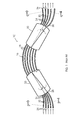
- FIG. 3 shows an AWGR 50 according to the invention. Elements shown in FIG. 3 which are identified by the same reference numerals as corresponding elements shown in FIG. 1 may have similar constructions.
- AWGR 50 has a plurality of output waveguides 32 .
- the qth output waveguide 32 is situated at angle ⁇ q .
- the terms “output” and “input” are used only as names to distinguish different elements of AWGR 50 . The use of these terms does not impose any restriction on the direction in which light may propagate through AWGR 50 .
- light may enter an “input” waveguide and emerge through one or more “output” waveguides.
- Light may also enter AWGR 50 through an “output” waveguide and emerge through one or more “input” waveguides. In some applications light may propagate simultaneously through AWGR 50 in opposing directions.
- Prior art AWGs are generally designed so that R has a small value.
- R is typically about 2 ⁇ / ⁇ where ⁇ is the channel spacing in frequency and ⁇ is the optical frequency.
- ⁇ is the channel spacing in frequency
- ⁇ is the optical frequency.
- AWGRs according to this invention are constructed so that R oscillates.
- R is a periodic function of q.
- R has a maximum value of at least 0.1. Preferably R does not have a value exceeding 0.01 for any two successive values of q.
- the angular separation of the output waveguides is not uniform. In some preferred embodiments of the invention, the angular separation of the output waveguides is a periodic function of q.
- s is a positive integer
- e is a number between zero and unity (preferably e is greater than about 0.1).
- the plurality of output waveguides is preferably centered at the pole of the output focal curve, which is directly opposite the AWG grating region. That is, preferably:
- the plurality of input waveguides is centered at the pole of the input focal curve, which is directly opposite the AWG grating region. That is, preferably:
- n s d ( ⁇ 0 + ⁇ 0 ) m ′( ⁇ 0 ⁇ c ) (21)
- AWGR 50 has a layout resembling that of an N ⁇ M router.
- the construction of AWGR 50 is such that AWGR 50 can function as N independent 1 ⁇ Q demultiplexers.
- output waveguides 32 are divided into N groups.
- the output waveguides of each of the groups are used in conjunction with one of the input waveguides.
- n s d ( ⁇ p + ⁇ q ) m′ ⁇ q+m ′( ⁇ 0 ⁇ c ) (23)
- the angular separation between adjacent output waveguides 32 is not a slowly varying function of q. Instead, the angular separation is a periodic function of q which has a period N. According to Equation 13, the angular separation between output waveguides is equal to: ( m ′ ⁇ ⁇ ⁇ ⁇ ⁇ n s ⁇ d )
- the angular separation between two adjacent waveguides when one waveguide is in one band and the other waveguide is in an adjacent band is equal to ( 1 + s + e ) ⁇ ( m ′ ⁇ ⁇ ⁇ ⁇ ⁇ n s ⁇ d ) .
- the value of R when q+2, q+1 and q identify output waveguides within a common band, and n s is independent of wavelength, the value of R is zero. When one of the output waveguides identified by the indices q+2, q+1 and q is in one band and the other two are in another band, then the value of R is approximately equal to (s+e), which is typically larger than unity.
- FIG. 4 is a schematic block diagram of a 2 ⁇ 6 AWGR 50 A according to this embodiment of the invention.
- AWGR 50 A can function as 2 independent 1 ⁇ 3 demultiplexers which operate on different bands.
- the three outputs for each band are physically clustered together, emerge from AWGR 50 A in wavelength sequence and are separated from the outputs for other bands.
- the outputs from one band are not interleaved with outputs from other bands.
- additional output waveguides are provided. These additional waveguides (which may be called “dummy” waveguides) do not need to be connected to output ports. Typically, relatively little light enters the dummy waveguides. Light that does enter a dummy waveguide is preferably allowed to radiate from the dummy waveguide in a manner that minimizes the amount of light that can cross over to any of output waveguides 32 . The light may radiate from the dummy waveguide gradually over a distance or in a concentrated manner at a termination point.
- the purpose of the dummy waveguides is to improve the uniformity with which output waveguides 32 can be fabricated. Without dummy waveguides those output waveguides 32 which lie at one end of a band have a different environment from those output waveguides 32 which lie within a band.
- the AWGR of FIG. 3 may be applied, for example, in the multi-band demultiplexer 70 shown in FIG. 6 A.
- the Q outputs of demultiplexer 72 are each connected to one of the Q inputs of an AWGR 50 according to the invention.
- This improves on prior art multi-stage demultiplexers in which the second stage is implemented using Q individual 1 ⁇ M demultiplexers.
- an AWGR 50 according to this embodiment of the invention is convenient because the output waveguides for each band are clustered together and are adjacent to one another.
- optical switches 74 may be inserted between one or more of the output ports of demultiplexer 72 and the corresponding input ports of AWGR 50 . It can be appreciated that a single optical switch permits an entire band of channels to be redirected.
- a second embodiment of the invention provides an AWGR 50 having (Q+G ⁇ 1) ⁇ N output waveguides and G ⁇ N input waveguides.
- g is an integer selected from a predetermined set of integers. In one embodiment g ⁇ 1, 0, 1 ⁇ :
- G is the number of members in the set from which g is selected.
- the input waveguides are divided into groups with each group of input waveguides associated with a specific value of g. For each value of g there is a target set of output waveguides.
- the target sets of output waveguides are each divided into N bands with Q passbands within each of the N bands.
- FIG. 5A is a block diagram representation of a simple AWGR 50 B according to this embodiment of the invention.
- AWGR 50 B has ten output waveguides in two groups. Each group of output waveguides corresponds to one of the groups of input waveguides.
- each output waveguide is used in conjunction with one of the input waveguides.
- Those input waveguides which are available, but not being used, may be called auxiliary waveguides.
- n s d ( ⁇ p,g + ⁇ q,g ) ( m ′ ⁇ )( q )+ m ′( ⁇ g ⁇ + ⁇ 0 ⁇ c ) (29).
- the wavelength coupled to each channel can be increased by an amount ⁇ g.
- the passbands fall on a wavelength grid according to
- an AWGR according to this embodiment of the invention provides N 1 ⁇ Q multiplexers (or demultiplexers) each having a grid of wavelengths which can be tuned by selecting an input waveguide corresponding to an appropriate value for g. The potential value of this is apparent from the discussion in the background section of this disclosure.
- the value of R when q+2, q+1 and q identify output waveguides within a common band, and n s is independent of wavelength, the value of R is zero. When one of the output waveguides identified by the indices q+2, q+1 and q is in one band and the other two are in another band, then the value of R is approximately equal to (s+e), which is typically larger than 1.
- Dummy waveguides may also be provided in this embodiment of the invention substantially as described above.
- the maximum value of R will be approximately e, which is typically larger than 0.1.
- c is the speed of light in vacuum
- n s ⁇ d ⁇ ( ⁇ p + ⁇ q ) ( m ′ ⁇ c ) ⁇ [ 1 ⁇ 0 - q ⁇ ⁇ ⁇ ⁇ ⁇ ⁇ - 1 ⁇ 0 + ⁇ 0 - ⁇ c ] ( 34 )
- this embodiment is similar to the first embodiment described above except that the passbands are on a frequency grid rather than a wavelength grid, i.e., the optical frequencies of the passbands are given by:
- the value of R is given approximately by ⁇ / ⁇ which is typically less than 0.001.
- the value of R is approximately equal to (s+e), which is typically larger than unity.
- a fourth example embodiment of the invention provides an AWGR 50 having (Q+G ⁇ 1) ⁇ N output waveguides and G ⁇ N input waveguides.
- g is an integer selected from a predetermined set of integers. In one embodiment g ⁇ 1, 0, 1 ⁇ ;
- G is the number of members of the set from which g is selected.
- n s ⁇ d ⁇ ( ⁇ p , g + ⁇ q , g ) ( m ′ ⁇ c ) ⁇ [ 1 v 0 - q ⁇ ⁇ ⁇ ⁇ ⁇ v - 1 v 0 + ⁇ 0 - ⁇ c + ⁇ ⁇ ⁇ g ] ( 38 )
- changing g in value from 0 to 1 shifts all the passbands in wavelength by ⁇ and changing g in value from 0 to ⁇ 1, shifts all the passbands in wavelength by ⁇ .
- the passbands are not precisely on the a frequency grid; nevertheless, in some applications this shift in wavelength can be used to reduce the discrepancy between the optical frequency of a particular passband and the desired optical frequency for that passband.
- the overall performance will be different for different values of g and the AWGR can be tuned by selecting a value for g that provides for the best overall performance in a specific application.
- a component e.g. an assembly, device, waveguide, coupler, etc.
- reference to that component should be interpreted as a reference to any component which performs the function of the described component (i.e., that is functionally equivalent), including components which are not structurally equivalent to the disclosed structure which performs the function in the illustrated exemplary embodiments of the invention.
Landscapes
- Physics & Mathematics (AREA)
- Engineering & Computer Science (AREA)
- Microelectronics & Electronic Packaging (AREA)
- General Physics & Mathematics (AREA)
- Optics & Photonics (AREA)
- Optical Integrated Circuits (AREA)
Abstract
Description


Claims (43)


Priority Applications (1)
| Application Number | Priority Date | Filing Date | Title |
|---|---|---|---|
| US09/970,207 US6678446B1 (en) | 2001-10-03 | 2001-10-03 | Multi-band arrayed waveguide grating |
Applications Claiming Priority (1)
| Application Number | Priority Date | Filing Date | Title |
|---|---|---|---|
| US09/970,207 US6678446B1 (en) | 2001-10-03 | 2001-10-03 | Multi-band arrayed waveguide grating |
Publications (1)
| Publication Number | Publication Date |
|---|---|
| US6678446B1 true US6678446B1 (en) | 2004-01-13 |
Family
ID=29780822
Family Applications (1)
| Application Number | Title | Priority Date | Filing Date |
|---|---|---|---|
| US09/970,207 Expired - Lifetime US6678446B1 (en) | 2001-10-03 | 2001-10-03 | Multi-band arrayed waveguide grating |
Country Status (1)
| Country | Link |
|---|---|
| US (1) | US6678446B1 (en) |
Cited By (16)
| Publication number | Priority date | Publication date | Assignee | Title |
|---|---|---|---|---|
| US20040264857A1 (en) * | 2003-06-27 | 2004-12-30 | Lucent Technologies Inc. | Arrayed waveguide gratings with improved transmission efficiency |
| US20050213883A1 (en) * | 2001-10-09 | 2005-09-29 | Infinera Corporation | Method of optimizing optical channel signal demultiplexing in a monolithic receiver photonic integrated circuit (RxPIC) |
| US20070065076A1 (en) * | 2005-09-21 | 2007-03-22 | Andevices, Inc. | Duplex arrayed waveguide grating |
| US20070122081A1 (en) * | 2005-11-30 | 2007-05-31 | Lucent Technologies Inc. | Improved waveguide structure |
| US20080253716A1 (en) * | 2007-03-28 | 2008-10-16 | The Furukawa Electric Co, Ltd. | Arrayed waveguide grating optical multiplexer/demultiplexer |
| US20090185806A1 (en) * | 2008-01-23 | 2009-07-23 | Andevices, Inc. | Broadcasting arrayed waveguide |
| US20120087667A1 (en) * | 2010-10-12 | 2012-04-12 | Hindrik Freerk Bulthuis | Awg supporting multiple frequency bands and channel plans |
| US20130223841A1 (en) * | 2012-02-29 | 2013-08-29 | National Taiwan University Of Science And Technology | Time/wavelength-division multiplexed passive optical network (twpon) |
| US8538212B2 (en) | 2011-06-03 | 2013-09-17 | Neophotonics Corporation | Thermally compensated arrayed waveguide grating assemblies |
| US8565600B2 (en) | 2011-06-10 | 2013-10-22 | Neophotonics Corporation | Optical network configurations with multiple band multiplexing and de-multiplexing and AWG structures with multiple band processing |
| CN104238008A (en) * | 2014-09-10 | 2014-12-24 | 浙江大学 | N*N array waveguide grating optical wavelength router capable of reducing frequency deviation |
| US9110232B2 (en) | 2011-06-03 | 2015-08-18 | Neophotonics Corporation | Thermally compensated arrayed waveguide grating assemblies |
| CN106605340A (en) * | 2015-08-18 | 2017-04-26 | 古河电气工业株式会社 | Photo-semiconductor device |
| WO2018085360A1 (en) * | 2016-11-01 | 2018-05-11 | Sb Microsystems | Selective arrayed waveguide spectrometer |
| WO2019111718A1 (en) * | 2017-12-06 | 2019-06-13 | Nttエレクトロニクス株式会社 | Optical wavelength multiplexer/demultiplexer |
| WO2022218178A1 (en) * | 2021-04-15 | 2022-10-20 | 华为技术有限公司 | Arrayed waveguide grating |
Citations (7)
| Publication number | Priority date | Publication date | Assignee | Title |
|---|---|---|---|---|
| US5136671A (en) * | 1991-08-21 | 1992-08-04 | At&T Bell Laboratories | Optical switch, multiplexer, and demultiplexer |
| US5845022A (en) * | 1997-02-14 | 1998-12-01 | Doerr; Christopher Richard | Double-chirped waveguide grating router with angled ports |
| US6058233A (en) * | 1998-06-30 | 2000-05-02 | Lucent Technologies Inc. | Waveguide array with improved efficiency for wavelength routers and star couplers in integrated optics |
| US6381383B1 (en) * | 2000-04-24 | 2002-04-30 | Agere Systems Guardian Corp | Large N×N waveguide grating router |
| US6389201B1 (en) * | 1999-10-14 | 2002-05-14 | Nec Corporation | Arrayed waveguide grating having arrayed waveguide employing taper structure |
| US20020057875A1 (en) * | 2000-11-16 | 2002-05-16 | Tarou Kaneko | Array waveguide grating, optical transmitter and optical communication system with monitoring function |
| US6512864B1 (en) * | 2000-06-08 | 2003-01-28 | Lucent Technologies Inc. | Optical multiplexer/demultiplexer arrangement for WDM signals having in-band and out-of-band signal components |
-
2001
- 2001-10-03 US US09/970,207 patent/US6678446B1/en not_active Expired - Lifetime
Patent Citations (8)
| Publication number | Priority date | Publication date | Assignee | Title |
|---|---|---|---|---|
| US5136671A (en) * | 1991-08-21 | 1992-08-04 | At&T Bell Laboratories | Optical switch, multiplexer, and demultiplexer |
| US5845022A (en) * | 1997-02-14 | 1998-12-01 | Doerr; Christopher Richard | Double-chirped waveguide grating router with angled ports |
| US6058233A (en) * | 1998-06-30 | 2000-05-02 | Lucent Technologies Inc. | Waveguide array with improved efficiency for wavelength routers and star couplers in integrated optics |
| US6389201B1 (en) * | 1999-10-14 | 2002-05-14 | Nec Corporation | Arrayed waveguide grating having arrayed waveguide employing taper structure |
| US6381383B1 (en) * | 2000-04-24 | 2002-04-30 | Agere Systems Guardian Corp | Large N×N waveguide grating router |
| US6549698B2 (en) * | 2000-04-24 | 2003-04-15 | Agere Systems Guardian Corp. | Large N×N waveguide grating router |
| US6512864B1 (en) * | 2000-06-08 | 2003-01-28 | Lucent Technologies Inc. | Optical multiplexer/demultiplexer arrangement for WDM signals having in-band and out-of-band signal components |
| US20020057875A1 (en) * | 2000-11-16 | 2002-05-16 | Tarou Kaneko | Array waveguide grating, optical transmitter and optical communication system with monitoring function |
Cited By (29)
| Publication number | Priority date | Publication date | Assignee | Title |
|---|---|---|---|---|
| US20050213883A1 (en) * | 2001-10-09 | 2005-09-29 | Infinera Corporation | Method of optimizing optical channel signal demultiplexing in a monolithic receiver photonic integrated circuit (RxPIC) |
| US7158699B2 (en) * | 2001-10-09 | 2007-01-02 | Infinera Corporation | Method of optimizing optical channel signal demultiplexing in a monolithic receiver photonic integrated circuit (RxPIC) |
| US20040264857A1 (en) * | 2003-06-27 | 2004-12-30 | Lucent Technologies Inc. | Arrayed waveguide gratings with improved transmission efficiency |
| US6956993B2 (en) * | 2003-06-27 | 2005-10-18 | Lucent Technologies Inc. | Arrayed waveguide gratings with improved transmission efficiency |
| US20070065076A1 (en) * | 2005-09-21 | 2007-03-22 | Andevices, Inc. | Duplex arrayed waveguide grating |
| US7440655B2 (en) * | 2005-09-21 | 2008-10-21 | Andevices, Inc. | Duplex arrayed waveguide grating |
| US7330618B2 (en) * | 2005-11-30 | 2008-02-12 | Lucent Technologies Inc. | Waveguide structure |
| US20070122081A1 (en) * | 2005-11-30 | 2007-05-31 | Lucent Technologies Inc. | Improved waveguide structure |
| US20080253716A1 (en) * | 2007-03-28 | 2008-10-16 | The Furukawa Electric Co, Ltd. | Arrayed waveguide grating optical multiplexer/demultiplexer |
| US7542640B2 (en) * | 2007-03-28 | 2009-06-02 | The Furukawa Electric Co., Ltd. | Arrayed waveguide grating optical multiplexer/demultiplexer |
| US20090185806A1 (en) * | 2008-01-23 | 2009-07-23 | Andevices, Inc. | Broadcasting arrayed waveguide |
| US7639908B2 (en) * | 2008-01-23 | 2009-12-29 | Enablence USA Components, Inc. | Broadcasting arrayed waveguide |
| US20120087667A1 (en) * | 2010-10-12 | 2012-04-12 | Hindrik Freerk Bulthuis | Awg supporting multiple frequency bands and channel plans |
| US9494735B2 (en) * | 2010-10-12 | 2016-11-15 | Gemfire Corporation | AWG supporting multiple frequency bands and channel plans through respective multiple inputs |
| US8538212B2 (en) | 2011-06-03 | 2013-09-17 | Neophotonics Corporation | Thermally compensated arrayed waveguide grating assemblies |
| US9110232B2 (en) | 2011-06-03 | 2015-08-18 | Neophotonics Corporation | Thermally compensated arrayed waveguide grating assemblies |
| US8565600B2 (en) | 2011-06-10 | 2013-10-22 | Neophotonics Corporation | Optical network configurations with multiple band multiplexing and de-multiplexing and AWG structures with multiple band processing |
| US20130223841A1 (en) * | 2012-02-29 | 2013-08-29 | National Taiwan University Of Science And Technology | Time/wavelength-division multiplexed passive optical network (twpon) |
| CN104238008A (en) * | 2014-09-10 | 2014-12-24 | 浙江大学 | N*N array waveguide grating optical wavelength router capable of reducing frequency deviation |
| CN104238008B (en) * | 2014-09-10 | 2017-05-03 | 浙江大学 | N*N array waveguide grating optical wavelength router capable of reducing frequency deviation |
| CN106605340B (en) * | 2015-08-18 | 2020-07-10 | 古河电气工业株式会社 | Optical semiconductor device |
| CN106605340A (en) * | 2015-08-18 | 2017-04-26 | 古河电气工业株式会社 | Photo-semiconductor device |
| WO2018085360A1 (en) * | 2016-11-01 | 2018-05-11 | Sb Microsystems | Selective arrayed waveguide spectrometer |
| US10228513B2 (en) | 2016-11-01 | 2019-03-12 | Sb Microsystems | Selective arrayed waveguide spectrometer |
| WO2019111718A1 (en) * | 2017-12-06 | 2019-06-13 | Nttエレクトロニクス株式会社 | Optical wavelength multiplexer/demultiplexer |
| JP2019101315A (en) * | 2017-12-06 | 2019-06-24 | Nttエレクトロニクス株式会社 | Optical wavelength multiplexer/demultiplexer |
| CN111448498A (en) * | 2017-12-06 | 2020-07-24 | Ntt 电子股份有限公司 | Optical wavelength multiplexer/demultiplexer |
| US10983274B2 (en) * | 2017-12-06 | 2021-04-20 | Ntt Electronics Corporation | Optical wavelength multiplexer/demultiplexer |
| WO2022218178A1 (en) * | 2021-04-15 | 2022-10-20 | 华为技术有限公司 | Arrayed waveguide grating |
Similar Documents
| Publication | Publication Date | Title |
|---|---|---|
| US6678446B1 (en) | Multi-band arrayed waveguide grating | |
| US5450511A (en) | Efficient reflective multiplexer arrangement | |
| US5905824A (en) | Temperature compensated insensitive optical multiplexor/demultiplexor | |
| US6181849B1 (en) | Interleaved wavelengths multi/demultiplexer with multiple-input-ports and multiple-output-ports for wavelength add/drop WDM systems | |
| EP1857846B1 (en) | Asymmetric mach-zehnder interferometer having a reduced drive voltage coupled to a compact low-loss arrayed waveguide grating | |
| KR100383340B1 (en) | Optical passband filter | |
| JPH07301721A (en) | Frequency routing device | |
| US6526203B1 (en) | Arrayed waveguide grating with reduced crosstalk | |
| EP0823647B1 (en) | Arrayed-waveguide grating | |
| EP1251652A2 (en) | Arrayed waveguide grating optical multiplexer/demultiplexer | |
| US6668117B2 (en) | Arrayed waveguide grating optical multiplexer demultiplexer | |
| US6885823B2 (en) | Wavelength multiplexing/demultiplexing unit, wavelength multiplexing/demultiplexing apparatus and wavelength multiplexing/demultiplexing method | |
| EP1373950B1 (en) | Arrayed waveguide grating | |
| US7003198B2 (en) | Integrateable band filter using waveguide grating routers | |
| US20020081062A1 (en) | Optical grating based multi-input demultiplexer for multiple sets of interleaved wavelength channels | |
| CN111448498B (en) | Optical wavelength multiplexer/demultiplexer | |
| US6560380B2 (en) | Planar lightwave circuit interleaver | |
| US6728447B2 (en) | Optical multiplexer/demultiplexer | |
| US6415072B1 (en) | Optical wavelength multiplexing and dividing device | |
| JPH0659291A (en) | Waveguide type optical multiplexer-branching filter for four-wave multiplex transmission and eight-wave multiple transmission | |
| US20230194780A1 (en) | Integrated Optical Structure for Multiplexing and/or Demultiplexing | |
| JP4238069B2 (en) | Optical wavelength multiplexer / demultiplexer | |
| US7010197B2 (en) | Integrateable band filter using waveguide grating routers | |
| EP1447693A1 (en) | Flexible Passband Filter | |
| CN115657202B (en) | Silicon-based wavelength demultiplexing device based on grating auxiliary reverse coupling |
Legal Events
| Date | Code | Title | Description |
|---|---|---|---|
| AS | Assignment |
Owner name: LIGHTWAVE MICROSYSTEMS CORPORATION, CALIFORNIA Free format text: ASSIGNMENT OF ASSIGNORS INTEREST;ASSIGNORS:MCGREER, KENNETH;LAM, JANE;REEL/FRAME:012231/0810 Effective date: 20011001 |
|
| STCF | Information on status: patent grant |
Free format text: PATENTED CASE |
|
| FEPP | Fee payment procedure |
Free format text: PAT HOLDER NO LONGER CLAIMS SMALL ENTITY STATUS, ENTITY STATUS SET TO UNDISCOUNTED (ORIGINAL EVENT CODE: STOL); ENTITY STATUS OF PATENT OWNER: LARGE ENTITY |
|
| FPAY | Fee payment |
Year of fee payment: 4 |
|
| AS | Assignment |
Owner name: NEOPHOTONICS CORPORATION,CALIFORNIA Free format text: ASSIGNMENT OF ASSIGNORS INTEREST;ASSIGNOR:LIGHTWAVE MICROSYSTEMS CORPORATION;REEL/FRAME:024505/0068 Effective date: 20100608 Owner name: NEOPHOTONICS CORPORATION, CALIFORNIA Free format text: ASSIGNMENT OF ASSIGNORS INTEREST;ASSIGNOR:LIGHTWAVE MICROSYSTEMS CORPORATION;REEL/FRAME:024505/0068 Effective date: 20100608 |
|
| FPAY | Fee payment |
Year of fee payment: 8 |
|
| FEPP | Fee payment procedure |
Free format text: PAYOR NUMBER ASSIGNED (ORIGINAL EVENT CODE: ASPN); ENTITY STATUS OF PATENT OWNER: LARGE ENTITY |
|
| FPAY | Fee payment |
Year of fee payment: 12 |