US6563544B1 - Combined vertical filter for graphic displays - Google Patents

Combined vertical filter for graphic displays Download PDF

Info

Publication number
US6563544B1
US6563544B1 US09/393,480 US39348099A US6563544B1 US 6563544 B1 US6563544 B1 US 6563544B1 US 39348099 A US39348099 A US 39348099A US 6563544 B1 US6563544 B1 US 6563544B1
Authority
US
United States
Prior art keywords
input
output
flicker
scaling
image
Prior art date
Legal status (The legal status is an assumption and is not a legal conclusion. Google has not performed a legal analysis and makes no representation as to the accuracy of the status listed.)
Expired - Lifetime
Application number
US09/393,480
Inventor
Maximino Vasquez
Current Assignee (The listed assignees may be inaccurate. Google has not performed a legal analysis and makes no representation or warranty as to the accuracy of the list.)
Intel Corp
Original Assignee
Intel Corp
Priority date (The priority date is an assumption and is not a legal conclusion. Google has not performed a legal analysis and makes no representation as to the accuracy of the date listed.)
Filing date
Publication date
Application filed by Intel Corp filed Critical Intel Corp
Priority to US09/393,480 priority Critical patent/US6563544B1/en
Assigned to CHIPS AND TECHNOLOGIES, LLC. reassignment CHIPS AND TECHNOLOGIES, LLC. ASSIGNMENT OF ASSIGNORS INTEREST (SEE DOCUMENT FOR DETAILS). Assignors: VASQUEZ, MAXIMINO
Assigned to INTEL CORPORATION reassignment INTEL CORPORATION ASSIGNMENT OF ASSIGNORS INTEREST (SEE DOCUMENT FOR DETAILS). Assignors: CHIPS AND TECHNOLOGIES, LLC
Application granted granted Critical
Publication of US6563544B1 publication Critical patent/US6563544B1/en
Anticipated expiration legal-status Critical
Expired - Lifetime legal-status Critical Current

Links

Images

Classifications

    • HELECTRICITY
    • H04ELECTRIC COMMUNICATION TECHNIQUE
    • H04NPICTORIAL COMMUNICATION, e.g. TELEVISION
    • H04N7/00Television systems
    • H04N7/01Conversion of standards, e.g. involving analogue television standards or digital television standards processed at pixel level
    • H04N7/0127Conversion of standards, e.g. involving analogue television standards or digital television standards processed at pixel level by changing the field or frame frequency of the incoming video signal, e.g. frame rate converter
    • H04N7/0132Conversion of standards, e.g. involving analogue television standards or digital television standards processed at pixel level by changing the field or frame frequency of the incoming video signal, e.g. frame rate converter the field or frame frequency of the incoming video signal being multiplied by a positive integer, e.g. for flicker reduction
    • HELECTRICITY
    • H04ELECTRIC COMMUNICATION TECHNIQUE
    • H04NPICTORIAL COMMUNICATION, e.g. TELEVISION
    • H04N7/00Television systems
    • H04N7/01Conversion of standards, e.g. involving analogue television standards or digital television standards processed at pixel level
    • H04N7/0117Conversion of standards, e.g. involving analogue television standards or digital television standards processed at pixel level involving conversion of the spatial resolution of the incoming video signal
    • H04N7/012Conversion between an interlaced and a progressive signal
    • YGENERAL TAGGING OF NEW TECHNOLOGICAL DEVELOPMENTS; GENERAL TAGGING OF CROSS-SECTIONAL TECHNOLOGIES SPANNING OVER SEVERAL SECTIONS OF THE IPC; TECHNICAL SUBJECTS COVERED BY FORMER USPC CROSS-REFERENCE ART COLLECTIONS [XRACs] AND DIGESTS
    • Y10TECHNICAL SUBJECTS COVERED BY FORMER USPC
    • Y10STECHNICAL SUBJECTS COVERED BY FORMER USPC CROSS-REFERENCE ART COLLECTIONS [XRACs] AND DIGESTS
    • Y10S348/00Television
    • Y10S348/91Flicker reduction

Definitions

  • the present invention relates to video displays. More particularly, the present invention relates to a combined vertical filter for processing computer graphic images.
  • a desirable feature for a multimedia computer system is the ability to display computer graphics on a standard television (TV) screen.
  • TV television
  • Table 1 the format and characteristics of the two systems differ.
  • Computer graphics images are typically noninterlaced. That is, the entire frame is stored, and displayed, line-by-line from top to bottom. The process repeats and the entire frame is re-scanned at a given refresh rate, for example 75 Hz.
  • TV formats typically use two interlaced fields to store and display an image. Each of the two frames contains every other line of the image, such as one with the even numbered lines and the other with the odd. The two fields are consecutively scanned, so that the viewer perceives the resulting image as a blend of the two individual fields.
  • the technique of interlacing was originally developed, in the early days of television, to present a pleasing graphic image while allowing a lower data transfer rate than needed to update the entire image with each scan. Although modern computer systems are not constrained by data transfer rates to the same extent as were early TV systems, interlaced display formats for TV are unlikely to disappear soon.
  • Overscan is also a remnant of early systems that is now firmly embedded in TV formats. Because it was costly to build TV picture tubes that accurately displayed an image along the outside border, overscan was developed to hide the image border. Typically, 10% to 20% of the image is cropped, or not displayed. For example, the NTSC format contains 486 active horizontal lines per frame but only approximately 430 lines are visible on a TV. Overscan compensation, which makes these hidden lines visible, may be needed when displaying computer graphics on a TV. For example, the “Start” icon displayed in Microsoft® Windows® that typically appears in the lower left corner of the computer monitor may be outside the displayed area of a TV screen without overscan compensation.
  • Computer graphics often contain images with high vertical frequency. That is, adjacent horizontal lines may have a high contrast, such as a light rectangular window displayed on a dark background.
  • High vertical frequency is less common in “natural images” created for display on a TV.
  • High vertical frequency may lead to a “flicker” effect when the image is displayed in an interlaced format on a TV.
  • the flicker effect is caused by the location of the horizontal edge shifting slightly as the two interlaced fields, the even lines and the odd lines, are consecutively scanned.
  • the present invention uses a flicker filter to reduce this effect.
  • Most TV displays do not include a flicker filter.
  • a computer system may be capable of generating, and displaying graphic images in multiple resolution, such as 640 ⁇ 480, 800 ⁇ 600, 1024 ⁇ 768 and 1280 ⁇ 960.
  • a TV display format is typically defined around a single resolution such as the 486 active horizontal lines used by the NTSC format.
  • a multimedia computer system would preferably not be limited to any one image resolution.
  • the present invention is directed at noninterlaced to interlaced conversion, vertical overscan compensation, vertical scaling, filtering high vertical frequency images and accepting computer graphic images in a variety of resolutions for display on a TV. While there are prior art techniques for individually performing these processes, the present invention efficiently combines the processes.
  • the last line of Table 1 describes two different color space formats that may be used by computer graphics and TV. These formats are well known to those of ordinary skill in the art, as are the formulas for converting between RGB and YUV color spaces. This conversion is not done by the present invention, although, the present invention may be used in conjunction with hardware or software that performs such a conversion. The present invention may be used with computer graphics using either RGB or YUV color spaces.
  • An apparatus and method for converting computer graphics images into a format suitable for display on a TV is combined with a vertical scaling filter and/or vertical overscan compensation filter to produce an interlaced image formatted for display on a TV, more efficiently than if the processes occurred sequentially.
  • the apparatus and method are not limited to any particular filter sizes or set of filter coefficient values. The apparatus and method may be used as part of a multimedia computer system.
  • FIG. 1 is a diagram depicting the filtering of an image with a 3-tap filter.
  • FIG. 2 is a data flow diagram of sequential flicker and scaling filters.
  • FIG. 3 is a data flow diagram in a combined filter in accordance with one embodiment of the present invention.
  • FIGS. 4A-C are timing diagrams of input and output for various scaling ratios.
  • FIG. 5 depicts scaling a noninterlaced input image and creating two scaled interlaced output frames.
  • the present invention converts computer graphic images into a format suitable for display on a standard television (TV) screen. It combines the processes of converting from noninterlaced to interlaced formats, vertical overscan compensation, flicker filtering and vertically scaling the size of an image. By combining these processes, the number of line buffers (memory) required, as well as the number of mathematical operations, are reduced compared to performing the operations separately. The invention thus allows the operations to be performed cheaper and faster. Alternatively, more sophisticated filtering could be performed on the image with same cost and speed as the prior art.
  • the present invention does not provide horizontal overscan compensation or horizontal scaling. However, the present invention may be used in conjunction with horizontal image processing devices or methods.
  • FIR filtering digital signals with finite impulse response (FIR) filters is a common practice in digital signal processing, and it is known to those of ordinary skill in the art.
  • An FIR filter can be described by the following transfer function:
  • H z ( z ) b o +b 1 z ⁇ 1 +. . . +b q z ⁇ q
  • H z (z) denotes the z-transform.
  • FIRs there are an infinite number of possible FIRs, each distinguished by the values assigned to the coefficients b n .
  • An FIR with a total of p non-zero coefficients is often referred to as a p-tap filter.
  • a p-tap vertical filter typically requires p- 1 lines of an image to be held in memory. This may be referred to as requiring p- 1 line buffers.
  • the present invention preferably uses an FIR as a flicker filter in situations where high vertical frequency is present in the computer graphics image.
  • a flicker filter may be a three-tap low pass filter, although, the present invention is not intended to be limited to any particular form of the filter.
  • Low pass filters as is known to those of ordinary skill in the art, are designed to pass low frequencies and block high frequencies.
  • Such a three-tap filter may take the form:
  • H 1 ( z ) c 1 +c 2 z ⁇ 1 +c 3 z ⁇ 2
  • FIG. 1 a three-tap flicker filter is shown operating on an image.
  • the filter coefficients 10 and 12 operate vertically on horizontal lines of image n ⁇ 1 through n+2, denoted by reference numbers 14 , 16 , 18 and 20 . Although the filtering is typically performed for each location within a horizontal line, FIG. 1 concentrates on a single horizontal position denoted as x.
  • filter coefficients 10 are applied to three vertically adjacent lines of the image, n ⁇ 1 14 , n 16 , and n+1 18 , to produce filtered line n 22 .
  • filter coefficients 12 are applied to lines n 16 , n+1 18 , and n+2 20 , to produce filtered line n+1 24 .
  • filter coefficients 10 are “shifted down” one line where they become filter coefficients 12 .
  • the three-tap flicker filter uses a weighted average of three vertically adjacent of the unfiltered image to decrease any large differences between adjacent lines.
  • the embodiment shown in FIG. 1 does not filter horizontally adjacent data, only those at location x.
  • the procedure depicted in FIG. 1 is repeated for each x value in a horizontal line of image data, such as x ⁇ 1 and x+1.
  • filtering techniques such as five-tap low pass filters, could also be used to reduce flicker.
  • increasing the complexity of a filter typically requires more memory and processing operations. While increasing the complexity of a filter may well increase the quality of the filtered image, there are typically diminishing returns.
  • a three-tap flicker filter is chosen as a reasonable balance between image quality, memory requirements and processing speed.
  • Conversion of an image from noninterlaced to interlaced formats may also be performed with filters such as FIRs.
  • FIRs filters
  • the simplest form of noninterlaced to interlaced conversion would be to skip every other line while creating an interlaced video frame. For example, use odd numbered lines for the first frame and even numbered lines for the second. Of course, more complex conversions are also possible.
  • Vertical scaling and overscan compensation can be combined with the noninterlaced to interlaced conversion process, using a single filter.
  • This disclosure will use the term scaling filter to describe noninterlaced to interlaced conversion, vertically scaling an image, and vertically compensating for overscan of an image.
  • Such a scaling filter could perform any one, or any combination of two or more of the processes.
  • the scaling filter however, only operates in the vertical direction on an image.
  • Horizontal scaling, such as compensating for horizontal overscan may be required, but will not be a part of the present invention.
  • the present invention may, however, be adapted to work in conjunction with a horizontal scaling and the present invention is not intended to be limited to images that do not require horizontal scaling.
  • a two-tap FIR scaling filter is used, taking the form:
  • the coefficients include the subscript “y” to denote that they may take on different values, at different y-locations, or different image lines.
  • the coefficients satisfy the constraints:
  • FIG. 2 illustrates a prior art design of sequential flicker 26 and scaling 28 filters.
  • a 3-tap flicker filter 26 with coefficients c 1 , c 2 and C 3 , is followed by the application of a 2-tap scaling filter with coefficients d 1 and d 2 .
  • Line buffers 30 and 32 provide temporary storage for two lines of video input data; multipliers 34 , 36 and 38 , along with adder 40 , are used to combine the flicker filter coefficients with the video input data.
  • the flicker filtered data is then processed by the scaling filter 28 utilizing line buffers 42 and 44 , and multipliers 46 and 48 .
  • Temporary values are summed by adder 50 and placed in output line buffer 68 , for display.
  • the present invention combines both the flicker and scaling filters.
  • the resulting 5-tap filter requires only two line buffers, plus an output buffer.
  • the combined filter H(z) is found by the convolution, denoted as *, of H 1 (z) and H 2 (z).
  • FIG. 3 A diagram of one embodiment of the present invention, used to implement a combined 5-tap filter, is shown as FIG. 3 .
  • This embodiment uses two line buffers, 54 and 56 , three multipliers 58 , 60 and 62 , two adders, 64 and 66 , and output buffer 68 .
  • Those of ordinary skill in the art will readily recognize that eliminating two line buffers and two multipliers, compared with sequential flicker and scaling filters, results in significant savings in terms of both component cost and processing time.
  • multiplexers 70 , 72 and 74 are required by the combined filter, these components are relatively inexpensive and do not significantly slow the throughput of the filter.
  • the present invention unlike conventional designs, uses line buffers 54 and 56 for temporary storage during filtering. It also exploits the inherent fact that interlaced output occurs at one-half the rate that noninterlaced data is input to efficiently order the processing.
  • Table 2 lists an example of the data in line buffers 54 and 56 and to output buffer 68 with each line of input for the combined filter shown by FIG. 3 . Preferably, the calculations are done for an entire horizontal line at one time.
  • C 1 ⁇ I(n) denotes that coefficient C 1 is multiplied by the array of values presenting line “n.”
  • the values of the coefficients may vary with the input line.
  • the value of C 1 used with I(1) may not be the same as the value of C 1 used with I(9).
  • a control scheme is required for a combined filter in order to synchronize the input data stream with the output.
  • noninterlaced to interlaced conversion produces output at one-half the rate of the input.
  • Two other factors also affect the timing of input and output: differences in refresh rate and overscan compensation/scaling.
  • the computer graphic image may have been created for a 75 Hz noninterlaced refresh rate, while the TV format is an interlaced 60 Hz.
  • overscan compensation/scaling can effect the synchronization between the input and output data.
  • One embodiment of the present invention uses an output clock and a demand based input stream capable of supplying data at four times the rate of the output clock.
  • SF max Maximum ⁇ ⁇ Input ⁇ ⁇ Speed Output ⁇ ⁇ Clock ⁇ ⁇ Speed
  • the clock speed selected for a particular application would preferably be based on the range of anticipated scaling.
  • FIGS. 4A-4C Timing diagrams for various scaling ratios are shown in FIGS. 4A-4C.
  • the input data 80 must be fast enough to “keep up with” the output data 82 .
  • stalling of the input data 80 is one technique that could be used to keep the input data 80 and output date 82 synchronized.
  • Each block of the output data 82 indicates a single line is sent to output buffer 68 .
  • Each block of the input data 80 indicates a single line of data is read, a “w” indicates a write to the output buffer.
  • Overscan compensation and scaling is somewhat similar to noninterlaced to interlaced data conversion. However, unlike noninterlaced to interlaced conversions, there is seldom a 2:1 ratio between the input and output data.
  • Overscan compensation can be handled in many ways.
  • TV formats typically crop a fixed number of horizontal lines of image data. While this technique is easy to implement, it may not produce satisfactory displays of computer generated graphics.
  • using an n-tap filter, with n equal to the number of lines in the original image, for overscan compensation is costly. For example, a 1280 ⁇ 1024 resolution computer image would require a 1024-tap filter. The processing required for such a filter would be extremely difficult to accomplish in real time for a reasonable price.
  • One embodiment of the present invention uses a 5-tap filter for the combined flicker and overscan compensation filter.
  • Other size filters could be used, and the present invention is not intended to be limited to any particular combined filter.
  • phase is used to filter the input data and create output data.
  • the phase is used to track a fractional position while mapping the input lines to the output lines.
  • One embodiment of the present invention uses 16 phases, represented as 4 bits, when scaling. That is, non-integer mapping between input and output lines has an effective resolution of ⁇ fraction (1/16) ⁇ the distance between input lines.
  • Filter coefficients C 1 through C 5 may change depending on the particular input line number. With 16 phases, there are 16 sets of filter coefficients. With a 5-tap filter, 5 ⁇ 16 phase gives a total of 80 coefficients. Because of symmetry, only 9 sets of coefficients are unique and are stored. The present invention is not intended to be limited to any particular number of phases, or sets of filter coefficients.
  • One embodiment of the present invention uses a digital differential analyzer (DDA) to determine which lines of input to use in the filter function for a particular line of output.
  • the DDA is a counter that increments for every output line.
  • the DDA indicates which input lines and filter phase to use.
  • InputPos is the input line position, with the integer portion representing the input line number and the fractional portion the filter phase.
  • InitPhase is the initial phase.
  • SF is the scale factor, the number of input lines divided by the number of output lines in a field.
  • the variable n represents the current output line being produced. Odd and even output fields have differing initial phases. For even numbered output fields, the initial phase is adjusted by adding 0.5 times SF to the initial phase for odd output fields.
  • FIG. 5 depicts a mapping from a noninterlaced input frame 84 to two interlaced output frames 86 and 88 using a 5-tap filter.
  • the first output frame, or the “odd field”, is shown with solid lines 86 .
  • the even field is shown as broken lines 88 .
  • the distance between lines is scaled by SF/2.
  • the initial line can be thought of being offset from the top of the frame by 1 ⁇ 2 line.
  • the initial phase for an even output field is (SF/4 ⁇ 0.5)+0.5 * SF, which is equal to 3 * SF/4 ⁇ 0.5.
  • Processing the input image with a 5-tap filter requires some adjustment at the top and bottom lines of the image.
  • the top line is effectively duplicated and the filter coefficients are applied to the duplicate lines. That is, (c 1 +c 2 +c 3 ) is multiplied by I(1).
  • Other “missing lines” are processed in a similar fashion.
  • the present invention is not, however, intended to be limited to any particular method of filtering the boundaries of an image.
  • the combined filter must be separately applied to each component of a video image, such as the three components of a color image.
  • the present invention may be used with any colorspace format, such as RGB or YUV, without modification.

Abstract

An apparatus and method for converting computer graphics images into a format suitable for display on a TV. A flicker filter is combined with a vertical scaling filter and/or vertical overscan compensation filter to produce an interlaced image formatted for display on a TV, more efficiently than if the processes occurred sequentially. The apparatus and method are not limited to any particular filter sizes or set of filter coefficient values. The apparatus and method may be used as part of a multimedia computer system.

Description

BACKGROUND OF THE INVENTION
1. Field of the Invention
The present invention relates to video displays. More particularly, the present invention relates to a combined vertical filter for processing computer graphic images.
2. The Background Art
A desirable feature for a multimedia computer system is the ability to display computer graphics on a standard television (TV) screen. However, the format and characteristics of the two systems differ. Some of the differences are listed in Table 1.
TABLE 1
Computer Graphics TV
Noninterlaced Interlaced
Display Entire Frame Overscan
High Vertical Frequency is Common Low Vertical Frequency
Multiple Resolution Fixed Resolution
RGB 444 Format YUV 422 Format
Omitted from Table 1, and this disclosure, are details particular to the various formats of TV such as National Television Standards Committee (NTSC), Phase Alternative Line (PAL) and Sequential Couleur Avec Mémoire (SECAM). Those of ordinary skill in the art are familiar with conversions between the various TV formats and the present invention is not intended to be limited to use with any particular format.
Computer graphics images are typically noninterlaced. That is, the entire frame is stored, and displayed, line-by-line from top to bottom. The process repeats and the entire frame is re-scanned at a given refresh rate, for example 75 Hz. In contrast, TV formats typically use two interlaced fields to store and display an image. Each of the two frames contains every other line of the image, such as one with the even numbered lines and the other with the odd. The two fields are consecutively scanned, so that the viewer perceives the resulting image as a blend of the two individual fields. The technique of interlacing was originally developed, in the early days of television, to present a pleasing graphic image while allowing a lower data transfer rate than needed to update the entire image with each scan. Although modern computer systems are not constrained by data transfer rates to the same extent as were early TV systems, interlaced display formats for TV are unlikely to disappear soon.
Overscan is also a remnant of early systems that is now firmly embedded in TV formats. Because it was costly to build TV picture tubes that accurately displayed an image along the outside border, overscan was developed to hide the image border. Typically, 10% to 20% of the image is cropped, or not displayed. For example, the NTSC format contains 486 active horizontal lines per frame but only approximately 430 lines are visible on a TV. Overscan compensation, which makes these hidden lines visible, may be needed when displaying computer graphics on a TV. For example, the “Start” icon displayed in Microsoft® Windows® that typically appears in the lower left corner of the computer monitor may be outside the displayed area of a TV screen without overscan compensation.
Computer graphics often contain images with high vertical frequency. That is, adjacent horizontal lines may have a high contrast, such as a light rectangular window displayed on a dark background. High vertical frequency is less common in “natural images” created for display on a TV. High vertical frequency may lead to a “flicker” effect when the image is displayed in an interlaced format on a TV. The flicker effect is caused by the location of the horizontal edge shifting slightly as the two interlaced fields, the even lines and the odd lines, are consecutively scanned. The present invention uses a flicker filter to reduce this effect. Most TV displays do not include a flicker filter.
Another issue when displaying computer graphics on a TV is that of the multiple resolutions often used in computer displays and the fixed resolution of a given TV display format. That is, a computer system may be capable of generating, and displaying graphic images in multiple resolution, such as 640×480, 800×600, 1024×768 and 1280×960. However, a TV display format is typically defined around a single resolution such as the 486 active horizontal lines used by the NTSC format. In order to display a wide range of computer graphic images on a TV, a multimedia computer system would preferably not be limited to any one image resolution.
The present invention is directed at noninterlaced to interlaced conversion, vertical overscan compensation, vertical scaling, filtering high vertical frequency images and accepting computer graphic images in a variety of resolutions for display on a TV. While there are prior art techniques for individually performing these processes, the present invention efficiently combines the processes.
The last line of Table 1 describes two different color space formats that may be used by computer graphics and TV. These formats are well known to those of ordinary skill in the art, as are the formulas for converting between RGB and YUV color spaces. This conversion is not done by the present invention, although, the present invention may be used in conjunction with hardware or software that performs such a conversion. The present invention may be used with computer graphics using either RGB or YUV color spaces.
SUMMARY OF THE INVENTION
An apparatus and method for converting computer graphics images into a format suitable for display on a TV. A flicker filter is combined with a vertical scaling filter and/or vertical overscan compensation filter to produce an interlaced image formatted for display on a TV, more efficiently than if the processes occurred sequentially. The apparatus and method are not limited to any particular filter sizes or set of filter coefficient values. The apparatus and method may be used as part of a multimedia computer system.
BRIEF DESCRIPTION OF THE DRAWINGS
FIG. 1 is a diagram depicting the filtering of an image with a 3-tap filter.
FIG. 2 is a data flow diagram of sequential flicker and scaling filters.
FIG. 3 is a data flow diagram in a combined filter in accordance with one embodiment of the present invention.
FIGS. 4A-C are timing diagrams of input and output for various scaling ratios.
FIG. 5 depicts scaling a noninterlaced input image and creating two scaled interlaced output frames.
DETAILED DESCRIPTION OF A PREFERRED EMBODIMENT
Those of ordinary skill in the art will realize that the following description of the present invention is illustrative only and not in any way limiting. Other embodiments of the invention will readily suggest themselves to such skilled persons having the benefit of this disclosure.
The present invention converts computer graphic images into a format suitable for display on a standard television (TV) screen. It combines the processes of converting from noninterlaced to interlaced formats, vertical overscan compensation, flicker filtering and vertically scaling the size of an image. By combining these processes, the number of line buffers (memory) required, as well as the number of mathematical operations, are reduced compared to performing the operations separately. The invention thus allows the operations to be performed cheaper and faster. Alternatively, more sophisticated filtering could be performed on the image with same cost and speed as the prior art. The present invention does not provide horizontal overscan compensation or horizontal scaling. However, the present invention may be used in conjunction with horizontal image processing devices or methods.
Filtering digital signals with finite impulse response (FIR) filters is a common practice in digital signal processing, and it is known to those of ordinary skill in the art. An FIR filter can be described by the following transfer function:
H z(z)=b o +b 1 z −1 +. . . +b q z −q
where Hz(z) denotes the z-transform. The impulse response, h(n), of an FIR is h ( n ) = { b n if 0 n q 0 otherwise
Figure US06563544-20030513-M00001
There are an infinite number of possible FIRs, each distinguished by the values assigned to the coefficients bn. An FIR with a total of p non-zero coefficients is often referred to as a p-tap filter.
Generally, a higher number of taps allows more complex filtering at the cost of requiring more memory and arithmetic processes. In the context of video image processing, a p-tap vertical filter typically requires p-1 lines of an image to be held in memory. This may be referred to as requiring p-1 line buffers.
The present invention preferably uses an FIR as a flicker filter in situations where high vertical frequency is present in the computer graphics image. One form of such a flicker filter may be a three-tap low pass filter, although, the present invention is not intended to be limited to any particular form of the filter. Low pass filters, as is known to those of ordinary skill in the art, are designed to pass low frequencies and block high frequencies. Such a three-tap filter may take the form:
H 1(z)=c 1 +c 2 z −1 +c 3 z −2
where the coefficients are positive numbers and satisfy the constraint:
c 1 +c 2 +c 3=1
The impulse response h1(n) of the filter is h 1 ( n ) = { c 1 if n = 0 c 2 if n = 1 c 3 if n = 2 0 otherwise
Figure US06563544-20030513-M00002
For example, an FIR with c1=¼, c2=½, and c3=¼ is one embodiment of such a three-tap low pass flicker filter. There are many others.
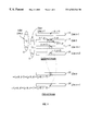
Referring to FIG. 1, a three-tap flicker filter is shown operating on an image. The filter coefficients 10 and 12 operate vertically on horizontal lines of image n−1 through n+2, denoted by reference numbers 14, 16, 18 and 20. Although the filtering is typically performed for each location within a horizontal line, FIG. 1 concentrates on a single horizontal position denoted as x. First, filter coefficients 10 are applied to three vertically adjacent lines of the image, n−1 14, n 16, and n+1 18, to produce filtered line n 22. Next, filter coefficients 12 are applied to lines n 16, n+1 18, and n+2 20, to produce filtered line n+1 24. That is, filter coefficients 10 are “shifted down” one line where they become filter coefficients 12. The three-tap flicker filter uses a weighted average of three vertically adjacent of the unfiltered image to decrease any large differences between adjacent lines. Those of ordinary skill in the art will readily recognize that varying the values of the filter coefficients will vary the amount of smoothing between lines. For example, coefficients c1=0, c2=1, and c3=0 would provide no smoothing.
The embodiment shown in FIG. 1 does not filter horizontally adjacent data, only those at location x. The procedure depicted in FIG. 1 is repeated for each x value in a horizontal line of image data, such as x−1 and x+1.
Other filtering techniques, such as five-tap low pass filters, could also be used to reduce flicker. As discussed above, increasing the complexity of a filter typically requires more memory and processing operations. While increasing the complexity of a filter may well increase the quality of the filtered image, there are typically diminishing returns. In one embodiment of the present invention, a three-tap flicker filter is chosen as a reasonable balance between image quality, memory requirements and processing speed. Those of ordinary skill in the art will readily recognize that such an engineering judgment in selecting a preferred filter size is subject to the current, and expected, costs of memory and processing.
Conversion of an image from noninterlaced to interlaced formats may also be performed with filters such as FIRs. The simplest form of noninterlaced to interlaced conversion would be to skip every other line while creating an interlaced video frame. For example, use odd numbered lines for the first frame and even numbered lines for the second. Of course, more complex conversions are also possible.
Vertical scaling and overscan compensation can be combined with the noninterlaced to interlaced conversion process, using a single filter. This disclosure will use the term scaling filter to describe noninterlaced to interlaced conversion, vertically scaling an image, and vertically compensating for overscan of an image. Such a scaling filter could perform any one, or any combination of two or more of the processes. The scaling filter, however, only operates in the vertical direction on an image. Horizontal scaling, such as compensating for horizontal overscan may be required, but will not be a part of the present invention. The present invention may, however, be adapted to work in conjunction with a horizontal scaling and the present invention is not intended to be limited to images that do not require horizontal scaling.
In one embodiment of the present invention a two-tap FIR scaling filter is used, taking the form:
H 2(z)=d 1,y +d 2,y z −2
The impulse response h2(n), of the filter is h 2 ( n ) = { d 1 , y if n = 0 d 2 , y if n = 2 0 otherwise
Figure US06563544-20030513-M00003
The coefficients include the subscript “y” to denote that they may take on different values, at different y-locations, or different image lines. The coefficients satisfy the constraints:
d 1,y +d 2,y−1
d 2,y=frac(Δ·y+d 0)
where do is the interpolation initial phase, Δ is the interpolation increment and y is an output line counter value. The term phase will be further described below. The function frac (x) returns the fractional portion of the argument X. For example,frac (5/4)=0.2.
FIG. 2 illustrates a prior art design of sequential flicker 26 and scaling 28 filters. A 3-tap flicker filter 26, with coefficients c1, c2 and C3, is followed by the application of a 2-tap scaling filter with coefficients d1 and d2. Line buffers 30 and 32 provide temporary storage for two lines of video input data; multipliers 34, 36 and 38, along with adder 40, are used to combine the flicker filter coefficients with the video input data. The flicker filtered data is then processed by the scaling filter 28 utilizing line buffers 42 and 44, and multipliers 46 and 48. Temporary values are summed by adder 50 and placed in output line buffer 68, for display.
The present invention combines both the flicker and scaling filters. In one embodiment the resulting 5-tap filter requires only two line buffers, plus an output buffer. Using the above flicker filter H1(z) and scaling filter H2(z), the combined filter H(z) is found by the convolution, denoted as *, of H1(z) and H2(z). H ( z ) = H 1 ( z ) * H 2 ( z ) = ( c 1 + c 2 z - 1 + c 3 z - 2 ) ( d 1 , y + d 2 , y z - 2 ) = c 1 d 1 , y + c 2 d 1 , y z - 1 + ( c 3 d 1 , y + c 1 d 2 , y ) z - 2 + c 2 d 2 , y z - 3 + c 3 d 2 , y z - 4 = C 1 + C 2 z - 1 C 3 z - 2 + C 4 z - 3 + C 5 z - 4
Figure US06563544-20030513-M00004
Where the subscript “y” has been dropped for simplicity, although the coefficients can take on different values at different y locations.
A diagram of one embodiment of the present invention, used to implement a combined 5-tap filter, is shown as FIG. 3. This embodiment uses two line buffers, 54 and 56, three multipliers 58, 60 and 62, two adders, 64 and 66, and output buffer 68. Those of ordinary skill in the art will readily recognize that eliminating two line buffers and two multipliers, compared with sequential flicker and scaling filters, results in significant savings in terms of both component cost and processing time. Although multiplexers 70, 72 and 74 are required by the combined filter, these components are relatively inexpensive and do not significantly slow the throughput of the filter.
The present invention, unlike conventional designs, uses line buffers 54 and 56 for temporary storage during filtering. It also exploits the inherent fact that interlaced output occurs at one-half the rate that noninterlaced data is input to efficiently order the processing. Table 2 lists an example of the data in line buffers 54 and 56 and to output buffer 68 with each line of input for the combined filter shown by FIG. 3. Preferably, the calculations are done for an entire horizontal line at one time. In Table 2, C1×I(n) denotes that coefficient C1 is multiplied by the array of values presenting line “n.”
TABLE 2
Input Write to First Write to Second Write to Output
Line Line Buffer Line Buffer Line Buffer
1 C1 × I(1)
2 Above + C2 ×
I(2)
3 Above + C3 × C1 × I(3)
I(3)
4 Above + C4 × Above + C2 × I(4)
I(4)
5 C1 × I(5) Above + C3 × I(5) Line 4, First Line Buffer +
C5 × I(5)
6 Above + C2 × Above + C4 × I(6)
I(6)
7 Above + C3 × C1 × I(7) Line 6, Second Line
I(7) Buffer + C5 × I(7)
8 Above + C4 × Above + C2 × I(8)
I(8)
9 C1 × I(9) Above + C3 × I(9) Line 8, First Line Buffer +
C5 × I(9)
As discussed above, the values of the coefficients may vary with the input line. For example, the value of C1 used with I(1) may not be the same as the value of C1 used with I(9).
Those of ordinary skill in the art will readily recognize that combined flicker and scaling filters need not be limited to 5-taps, such as shown in FIG. 3. However, other embodiments, such as 7-tap combined filters would require minor modifications to the data path of FIG. 3 and the buffer values of Table 2. Such modifications are within the abilities of those of ordinary skill in the art. The present invention is not intended to be limited to any particular size combined filter.
A control scheme is required for a combined filter in order to synchronize the input data stream with the output. For example, noninterlaced to interlaced conversion produces output at one-half the rate of the input. Two other factors also affect the timing of input and output: differences in refresh rate and overscan compensation/scaling. The computer graphic image may have been created for a 75 Hz noninterlaced refresh rate, while the TV format is an interlaced 60 Hz. Similarly, as will be discussed in detail below, overscan compensation/scaling can effect the synchronization between the input and output data.
Many techniques are available for controlling and synchronizing, such as using separate timing generators for input and output, or using a single timing generator for the output and a demand based input stream with a throttling mechanism. The present invention, however, is not intended to be limited to any particular control technique. One embodiment of the present invention uses an output clock and a demand based input stream capable of supplying data at four times the rate of the output clock. As will be seen below, there is a maximum scaling factor (SF) equal to the maximum speed of the input divided by the output clock speed. SF max = Maximum Input Speed Output Clock Speed
Figure US06563544-20030513-M00005
The clock speed selected for a particular application would preferably be based on the range of anticipated scaling.
Timing diagrams for various scaling ratios are shown in FIGS. 4A-4C. In each, the input data 80 must be fast enough to “keep up with” the output data 82. Those of ordinary skill in the art will readily recognize that stalling of the input data 80 is one technique that could be used to keep the input data 80 and output date 82 synchronized. Each block of the output data 82 indicates a single line is sent to output buffer 68. Each block of the input data 80 indicates a single line of data is read, a “w” indicates a write to the output buffer.
Overscan compensation and scaling is somewhat similar to noninterlaced to interlaced data conversion. However, unlike noninterlaced to interlaced conversions, there is seldom a 2:1 ratio between the input and output data.
Overscan compensation can be handled in many ways. TV formats typically crop a fixed number of horizontal lines of image data. While this technique is easy to implement, it may not produce satisfactory displays of computer generated graphics. At the other extreme, using an n-tap filter, with n equal to the number of lines in the original image, for overscan compensation is costly. For example, a 1280×1024 resolution computer image would require a 1024-tap filter. The processing required for such a filter would be extremely difficult to accomplish in real time for a reasonable price.
One embodiment of the present invention uses a 5-tap filter for the combined flicker and overscan compensation filter. Other size filters could be used, and the present invention is not intended to be limited to any particular combined filter.
Those of ordinary skill in the art will readily recognize that vertically scaling a computer image is conceptually very similar to vertical overscan compensation. In both operations, X lines of input are converting to Y lines of output. The principal difference is that ratio of X to Y in scaling may well exceed the 1.10 to 1.20 range typical in overscan compensation.
Because scaling factors (SF) are not always integers, the concept of a “phase” is used to filter the input data and create output data. The phase is used to track a fractional position while mapping the input lines to the output lines. One embodiment of the present invention uses 16 phases, represented as 4 bits, when scaling. That is, non-integer mapping between input and output lines has an effective resolution of {fraction (1/16)} the distance between input lines. Filter coefficients C1 through C5 may change depending on the particular input line number. With 16 phases, there are 16 sets of filter coefficients. With a 5-tap filter, 5×16 phase gives a total of 80 coefficients. Because of symmetry, only 9 sets of coefficients are unique and are stored. The present invention is not intended to be limited to any particular number of phases, or sets of filter coefficients.
One embodiment of the present invention uses a digital differential analyzer (DDA) to determine which lines of input to use in the filter function for a particular line of output. The DDA is a counter that increments for every output line. The DDA indicates which input lines and filter phase to use. The DDA makes the following calculation: Input Pos = Init Phase + i = 1 n SF
Figure US06563544-20030513-M00006
Where InputPos is the input line position, with the integer portion representing the input line number and the fractional portion the filter phase. InitPhase is the initial phase. SF is the scale factor, the number of input lines divided by the number of output lines in a field. The variable n represents the current output line being produced. Odd and even output fields have differing initial phases. For even numbered output fields, the initial phase is adjusted by adding 0.5 times SF to the initial phase for odd output fields.
FIG. 5 depicts a mapping from a noninterlaced input frame 84 to two interlaced output frames 86 and 88 using a 5-tap filter.
The first output frame, or the “odd field”, is shown with solid lines 86. The even field is shown as broken lines 88.
In mapping from the input frame space to the output frame space, the distance between lines is scaled by SF/2. In the input frame, the initial line can be thought of being offset from the top of the frame by ½ line. In the output frame, this distance from the initial line to the top of the frame is scaled, and becomes ½ * SF/2=SF/4. If the first input line is at location 0, the top of the image starts at −0.5. So the initial output line is at SF/4−0.5. This is the initial phase for an odd output field. The initial phase for an even output field is (SF/4−0.5)+0.5 * SF, which is equal to 3 * SF/4−0.5.
Processing the input image with a 5-tap filter requires some adjustment at the top and bottom lines of the image. In accordance with one embodiment of the present invention, the top line is effectively duplicated and the filter coefficients are applied to the duplicate lines. That is, (c1+c2+c3) is multiplied by I(1). Other “missing lines” are processed in a similar fashion. The present invention is not, however, intended to be limited to any particular method of filtering the boundaries of an image.
As will be readily recognized by those of ordinary skill in the art, the combined filter must be separately applied to each component of a video image, such as the three components of a color image. The present invention, however, may be used with any colorspace format, such as RGB or YUV, without modification.
Those of ordinary skill in the art will readily recognize that faster clock speeds will allow more “hardware efficient” embodiments of the present invention. For example, a single adder and a single multiplier could process the data flow of the embodiment of the present invention shown in FIG. 3, if the clock speed were fast enough. The present invention is not, however, intended to be limited to any particular clock speed or processor configuration.
While embodiments and applications of this invention have been shown and described, it would be apparent to those skilled in the art that many more modifications than mentioned above are possible without departing from the inventive concepts herein after a review of this disclosure. The invention, therefore, is not to be restricted except in the spirit of the appended claims.

Claims (25)

What is claimed is:
1. A non-sequential combined flicker-scaling filter apparatus for producing a TV formatted image, comprising:
an input data reader for reading image data from an input image;
a filter coefficient generator for supplying a set of filter coefficients responsive to said input image; and
a non-sequential flicker-scaling engine for simultaneously applying flicker reduction to said input image and vertically scaling said input image by combining said input image and said filter coefficients to produce an interlaced and filtered display image,
wherein said flicker-scaling engine uses at least a four tap filter.
2. A combined flicker-scaling filter apparatus in accordance with claim 1, wherein:
said flicker-scaling engine uses a 5 tap filter.
3. A combined flicker-scaling filter apparatus in accordance with claim 1, wherein:
said flicker-scaling engine uses not more than two line buffers and one output buffer.
4. A combined flicker-scaling filter apparatus in accordance with claim 1, wherein:
said flicker-scaling engine uses not more than three multipliers.
5. A combined flicker-scaling filter apparatus in accordance with claim 1, wherein:
said flicker-scaling engine uses not more than two adders.
6. A combined flicker-scaling filter apparatus in accordance with claim 1, wherein:
said flicker-scaling engine uses not more than three multipliers and uses not more than two adders.
7. A combined flicker-scaling filter apparatus in accordance with claim 1, wherein:
said filter coefficient generator supplies one of nine sets of filter coefficients responsive to a phase.
8. A combined flicker-scaling filter apparatus in accordance with claim 1, further comprising:
a timing generator for controlling the speed of said flicker-scaling engine for producing said interlaced and filtered display image.
9. A combined flicker-scaling filter apparatus in accordance with claim 8, wherein:
said input data reader is adapted to read image data faster than is required by said timing generator and said flicker-scaling engine.
10. A combined flicker-scaling filter apparatus in accordance with claim 1, wherein:
said flicker-scaling engine vertically scales said input image by a scale factor to interlace said input image.
11. A combined flicker-scaling filter apparatus in accordance with claim 1, wherein:
said flicker-scaling engine vertically scale said input image by a scale factor both to interlace said input image and to display all of said input image within the TV formatted image.
12. A combined flicker-scaling filter apparatus in accordance with claim 11, further comprising:
a timing generator for generating an input clock signal and an output clock signal, said input clock signal for controlling the speed of the input data reader, said output clock signal for controlling the speed of said flicker-scaling engine for producing said interlaced and filter display image.
13. A method for producing a TV formatted image, comprising:
reading lines of an input image;
filtering lines of said input image simultaneously for flicker reduction and vertical scaling with a non-sequential combined filter; and
creating an interlaced and filtered display image,
wherein filtering is performed using at least a four tap filter.
14. A method in accordance with claim 13, wherein:
filtering is performed using a 5 tap filter.
15. A method in accordance with claim 13, wherein:
filtering is performed using not more than two line buffers and one output buffer.
16. A method in accordance with claim 13, wherein:
filtering is performed with not more than three simultaneous multiplications.
17. A method in accordance with claim 13, wherein:
filtering is performed with not more than two simultaneous additions.
18. A method in accordance with claim 13, wherein:
filtering is performed with not more than three simultaneous multiplications and not more than two simultaneous additions.
19. A method in accordance with claim 13, further comprising:
selecting one of nine sets of filter coefficients for said combined filter based on a phase.
20. A method in accordance with claim 13, wherein:
creating said interlaced and filtered display image is controlled by a timing generator.
21. A method in accordance with claim 20, wherein:
reading lines of said input image is at a rate faster than is required for creating said interlaced and filtered display image as controlled by said timing generator.
22. A method in accordance with claim 13, wherein:
creating said interlaced and filtered display image is performed by vertically scaling said input image by a scale factor.
23. A method in accordance with claim 22, wherein:
vertically scaling said input image by a scale factor both creates an interlaced display image and re-sizes said input image to fit within the TV formatted display image.
24. A program storage device readable by a machine, tangibly embodying a program of instructions executable by the machine to perform a method for producing a TV formatting image, the method comprising:
reading lines of an input image;
filtering lines of said input image simultaneously for flicker reduction and vertical scaling with a non-sequential combined filter; and
creating an interlaced and filtered display image,
wherein filtering is performed using at least a four tap filter.
25. A combined flicker-scaling filter apparatus for producing a TV formatted image, comprising:
a first multiplier having a first input connected to an input node, a second input connected to a first coefficient node, and an output;
a second multiplier having a first input connected to the input node, a second input connected to a second coefficient node, and an output;
a third multiplier having a first input connected to the input node, a second input connected to the second coefficient node, and an output;
a first adder having a first input connected to the output of the second multiplier, a second input, and an output;
a second adder having a first input connected to the output of the third multiplier, a second input, and an output;
a first multiplexer having at least one input connected to the output of the first multiplier, at least one input connected to the output of the first adder, and an output;
a second multiplexer having at least one input connected to the output of the first multiplier, at least one input connected to the output of the second adder, and an output;
a first line buffer having an input connected to the output of the first multiplexer and an output connected to the second input of the first adder;
a second line buffer having an input connected to the output of the second multiplexer and an output connected to the second input of the second adder;
a third multiplexer having at least one input connected to the output of the first adder, at least one input connected to the output of the second adder, and an output; and
an output buffer having an input connected to the output of the third multiplexer and an output connected to an output node.
US09/393,480 1999-09-10 1999-09-10 Combined vertical filter for graphic displays Expired - Lifetime US6563544B1 (en)

Priority Applications (1)

Application Number Priority Date Filing Date Title
US09/393,480 US6563544B1 (en) 1999-09-10 1999-09-10 Combined vertical filter for graphic displays

Applications Claiming Priority (1)

Application Number Priority Date Filing Date Title
US09/393,480 US6563544B1 (en) 1999-09-10 1999-09-10 Combined vertical filter for graphic displays

Publications (1)

Publication Number Publication Date
US6563544B1 true US6563544B1 (en) 2003-05-13

Family

ID=23554862

Family Applications (1)

Application Number Title Priority Date Filing Date
US09/393,480 Expired - Lifetime US6563544B1 (en) 1999-09-10 1999-09-10 Combined vertical filter for graphic displays

Country Status (1)

Country Link
US (1) US6563544B1 (en)

Cited By (18)

* Cited by examiner, † Cited by third party
Publication number Priority date Publication date Assignee Title
US20030147011A1 (en) * 2000-07-08 2003-08-07 Gerhard Wischermann Device for reducing flicker defects
US20030174245A1 (en) * 2002-03-12 2003-09-18 Via Technologies, Inc. Clock signal synthesizer with multiple frequency outputs and method for synthesizing clock signal
US20030174247A1 (en) * 2002-03-12 2003-09-18 Via Technologies, Inc. Adaptive deflicker method and adaptive deflicker filter
US20030174246A1 (en) * 2002-03-12 2003-09-18 Via Technologies, Inc. Method and device for processing image data from non-interlacing type into interlacing one
US20030185463A1 (en) * 2001-09-10 2003-10-02 Wredenhagen G. Finn System and method of scaling images using adaptive nearest neighbour
US20040008281A1 (en) * 2002-07-15 2004-01-15 Eric Jeffrey Method and apparatus for flicker filtering interlaced display data
US6970207B1 (en) * 1999-08-24 2005-11-29 Stmicroelectronics S.A. Anti-flicker filtering process and system
US20060078055A1 (en) * 2004-10-13 2006-04-13 Sadayoshi Kanazawa Signal processing apparatus and signal processing method
US20060149802A1 (en) * 2005-01-04 2006-07-06 Shang-Chieh Wen Scaling filter and method thereof
US7259796B2 (en) * 2004-05-07 2007-08-21 Micronas Usa, Inc. System and method for rapidly scaling and filtering video data
US7408590B2 (en) * 2004-05-07 2008-08-05 Micronas Usa, Inc. Combined scaling, filtering, and scan conversion
US7411628B2 (en) * 2004-05-07 2008-08-12 Micronas Usa, Inc. Method and system for scaling, filtering, scan conversion, panoramic scaling, YC adjustment, and color conversion in a display controller
US20080309817A1 (en) * 2004-05-07 2008-12-18 Micronas Usa, Inc. Combined scaling, filtering, and scan conversion
US20090214136A1 (en) * 2008-02-22 2009-08-27 Chia-Yun Cheng Image processing apparatus for scaling an input image according to various image processing requirements and method thereof
US20100266219A1 (en) * 2009-04-17 2010-10-21 Mstar Semiconductor, Inc. Filter and Method for Removing Image Errors and Associated Display Circuit
US11057585B2 (en) * 2018-01-16 2021-07-06 Korea Advanced Institute Of Science And Technology Image processing method and device using line input and output
US11956569B2 (en) 2018-01-16 2024-04-09 Korea Advanced Institute Of Science And Technology Image processing method and device using a line-wise operation
US11962937B2 (en) 2018-01-16 2024-04-16 Korea Advanced Institute Of Science And Technology Method and device of super resolution using feature map compression

Citations (11)

* Cited by examiner, † Cited by third party
Publication number Priority date Publication date Assignee Title
US4233601A (en) 1977-04-04 1980-11-11 International Computers Limited Display system
US4385293A (en) 1979-12-10 1983-05-24 United Technologies Corporation Gray shade operation of a large AC plasma display panel
US4739313A (en) 1986-06-13 1988-04-19 Rich, Inc. Multilevel grey scale or composite video to RGBI decoder
US4766427A (en) 1984-10-15 1988-08-23 Matsushita Electric Industrial Co., Ltd. Display apparatus with display screen splitting function
US5422654A (en) 1991-10-17 1995-06-06 Chips And Technologies, Inc. Data stream converter with increased grey levels
US5914753A (en) * 1996-11-08 1999-06-22 Chrontel, Inc. Apparatus and method to convert computer graphics signals to television video signals with vertical and horizontal scaling requiring no frame buffers
US6061094A (en) * 1997-11-12 2000-05-09 U.S. Philips Corporation Method and apparatus for scaling and reducing flicker with dynamic coefficient weighting
US6067120A (en) * 1997-08-27 2000-05-23 Sharp Kabushiki Kaisha Video signal conversion device for reducing flicker in non-interlaced to interlaced signal conversion
US6094226A (en) * 1997-06-30 2000-07-25 Cirrus Logic, Inc. System and method for utilizing a two-dimensional adaptive filter for reducing flicker in interlaced television images converted from non-interlaced computer graphics data
US6281933B1 (en) * 1997-12-11 2001-08-28 Chrontel, Inc. Images in interlaced formats: a novel method of scan conversion for video imaging systems
US6320619B1 (en) * 1997-12-11 2001-11-20 Intel Corporation Flicker filter circuit

Patent Citations (11)

* Cited by examiner, † Cited by third party
Publication number Priority date Publication date Assignee Title
US4233601A (en) 1977-04-04 1980-11-11 International Computers Limited Display system
US4385293A (en) 1979-12-10 1983-05-24 United Technologies Corporation Gray shade operation of a large AC plasma display panel
US4766427A (en) 1984-10-15 1988-08-23 Matsushita Electric Industrial Co., Ltd. Display apparatus with display screen splitting function
US4739313A (en) 1986-06-13 1988-04-19 Rich, Inc. Multilevel grey scale or composite video to RGBI decoder
US5422654A (en) 1991-10-17 1995-06-06 Chips And Technologies, Inc. Data stream converter with increased grey levels
US5914753A (en) * 1996-11-08 1999-06-22 Chrontel, Inc. Apparatus and method to convert computer graphics signals to television video signals with vertical and horizontal scaling requiring no frame buffers
US6094226A (en) * 1997-06-30 2000-07-25 Cirrus Logic, Inc. System and method for utilizing a two-dimensional adaptive filter for reducing flicker in interlaced television images converted from non-interlaced computer graphics data
US6067120A (en) * 1997-08-27 2000-05-23 Sharp Kabushiki Kaisha Video signal conversion device for reducing flicker in non-interlaced to interlaced signal conversion
US6061094A (en) * 1997-11-12 2000-05-09 U.S. Philips Corporation Method and apparatus for scaling and reducing flicker with dynamic coefficient weighting
US6281933B1 (en) * 1997-12-11 2001-08-28 Chrontel, Inc. Images in interlaced formats: a novel method of scan conversion for video imaging systems
US6320619B1 (en) * 1997-12-11 2001-11-20 Intel Corporation Flicker filter circuit

Cited By (28)

* Cited by examiner, † Cited by third party
Publication number Priority date Publication date Assignee Title
US6970207B1 (en) * 1999-08-24 2005-11-29 Stmicroelectronics S.A. Anti-flicker filtering process and system
US7466364B2 (en) * 2000-07-08 2008-12-16 Thomson Licensing Device for reducing flicker defects
US20030147011A1 (en) * 2000-07-08 2003-08-07 Gerhard Wischermann Device for reducing flicker defects
US7142729B2 (en) * 2001-09-10 2006-11-28 Jaldi Semiconductor Corp. System and method of scaling images using adaptive nearest neighbor
US20030185463A1 (en) * 2001-09-10 2003-10-02 Wredenhagen G. Finn System and method of scaling images using adaptive nearest neighbour
US7102690B2 (en) 2002-03-12 2006-09-05 Via Technologies Inc. Clock signal synthesizer with multiple frequency outputs and method for synthesizing clock signal
US20030174246A1 (en) * 2002-03-12 2003-09-18 Via Technologies, Inc. Method and device for processing image data from non-interlacing type into interlacing one
US7061537B2 (en) * 2002-03-12 2006-06-13 Via Technologies, Inc. Adaptive deflicker method and adaptive deflicker filter
US7084925B2 (en) 2002-03-12 2006-08-01 Via Technologies, Inc. Method and device for processing image data from non-interlacing type into interlacing one
US20030174247A1 (en) * 2002-03-12 2003-09-18 Via Technologies, Inc. Adaptive deflicker method and adaptive deflicker filter
US20030174245A1 (en) * 2002-03-12 2003-09-18 Via Technologies, Inc. Clock signal synthesizer with multiple frequency outputs and method for synthesizing clock signal
US20040008281A1 (en) * 2002-07-15 2004-01-15 Eric Jeffrey Method and apparatus for flicker filtering interlaced display data
US7034887B2 (en) * 2002-07-15 2006-04-25 Seiko Epson Corporation Method and apparatus for flicker filtering interlaced display data
US20080309817A1 (en) * 2004-05-07 2008-12-18 Micronas Usa, Inc. Combined scaling, filtering, and scan conversion
US7259796B2 (en) * 2004-05-07 2007-08-21 Micronas Usa, Inc. System and method for rapidly scaling and filtering video data
US7408590B2 (en) * 2004-05-07 2008-08-05 Micronas Usa, Inc. Combined scaling, filtering, and scan conversion
US7411628B2 (en) * 2004-05-07 2008-08-12 Micronas Usa, Inc. Method and system for scaling, filtering, scan conversion, panoramic scaling, YC adjustment, and color conversion in a display controller
US20060078055A1 (en) * 2004-10-13 2006-04-13 Sadayoshi Kanazawa Signal processing apparatus and signal processing method
US20060149802A1 (en) * 2005-01-04 2006-07-06 Shang-Chieh Wen Scaling filter and method thereof
US20090214136A1 (en) * 2008-02-22 2009-08-27 Chia-Yun Cheng Image processing apparatus for scaling an input image according to various image processing requirements and method thereof
US20100266219A1 (en) * 2009-04-17 2010-10-21 Mstar Semiconductor, Inc. Filter and Method for Removing Image Errors and Associated Display Circuit
US8488898B2 (en) * 2009-04-17 2013-07-16 Mstar Semiconductor, Inc. Filter and method for removing image errors and associated display circuit
US11057585B2 (en) * 2018-01-16 2021-07-06 Korea Advanced Institute Of Science And Technology Image processing method and device using line input and output
US11412175B2 (en) 2018-01-16 2022-08-09 Korea Advanced Institute Of Science And Technology Super-resolution method and device using linewise operation
US11956569B2 (en) 2018-01-16 2024-04-09 Korea Advanced Institute Of Science And Technology Image processing method and device using a line-wise operation
US11962937B2 (en) 2018-01-16 2024-04-16 Korea Advanced Institute Of Science And Technology Method and device of super resolution using feature map compression
US11968472B2 (en) 2018-01-16 2024-04-23 Korea Advanced Institute Of Science And Technology Image pipeline processing method and device
US11974069B2 (en) 2018-01-16 2024-04-30 Korea Advanced Institute Of Science And Technology Image processing method and device using feature map compression

Similar Documents

Publication Publication Date Title
US6563544B1 (en) Combined vertical filter for graphic displays
US5574572A (en) Video scaling method and device
US6784942B2 (en) Motion adaptive de-interlacing method and apparatus
US6411333B1 (en) Format conversion using patch-based filtering
US6327000B1 (en) Efficient image scaling for scan rate conversion
US7477319B2 (en) Systems and methods for deinterlacing video signals
US6556193B1 (en) De-interlacing video images using patch-based processing
US6320619B1 (en) Flicker filter circuit
KR100629981B1 (en) Method and apparatus for video line multiplication with enhanced sharpness
JPH08190371A (en) Picture scaling filter and video scaling method
WO1998020670A2 (en) System for converting computer graphics to television format with scaling requiring no frame buffers
US6522339B1 (en) Resolution conversion method and device
JP4445122B2 (en) System and method for 2-tap / 3-tap flicker filtering
US7542053B2 (en) Methods and apparatus for re-scaling image by variable re-scaling factor
TW511073B (en) A method and apparatus in a computer system to generate a downscaled video image for display on a television system
US6374279B1 (en) System and method for increasing dual FIR filter efficiency
US7440030B2 (en) Method and apparatus for interlaced display of progressive video content
US8588553B2 (en) Scaling method and device for image signals
JP2003204502A (en) Video signal processing apparatus
JP3292233B2 (en) Interpolation processing circuit
JPH09182031A (en) Improved video processing system
JPH11187360A (en) Image processor
JPS62282377A (en) Picture enlargement processing circuit with interpolation
JPH1146352A (en) Image display device
JPS61149987A (en) Image display unit

Legal Events

Date Code Title Description
AS Assignment

Owner name: CHIPS AND TECHNOLOGIES, LLC., CALIFORNIA

Free format text: ASSIGNMENT OF ASSIGNORS INTEREST;ASSIGNOR:VASQUEZ, MAXIMINO;REEL/FRAME:010435/0060

Effective date: 19990927

AS Assignment

Owner name: INTEL CORPORATION, CALIFORNIA

Free format text: ASSIGNMENT OF ASSIGNORS INTEREST;ASSIGNOR:CHIPS AND TECHNOLOGIES, LLC;REEL/FRAME:011449/0081

Effective date: 20010103

STCF Information on status: patent grant

Free format text: PATENTED CASE

CC Certificate of correction
FEPP Fee payment procedure

Free format text: PAYOR NUMBER ASSIGNED (ORIGINAL EVENT CODE: ASPN); ENTITY STATUS OF PATENT OWNER: LARGE ENTITY

FPAY Fee payment

Year of fee payment: 4

REMI Maintenance fee reminder mailed
FPAY Fee payment

Year of fee payment: 8

SULP Surcharge for late payment

Year of fee payment: 7

FPAY Fee payment

Year of fee payment: 12