US6487260B1 - Method and apparatus for efficient correlation detection - Google Patents
Method and apparatus for efficient correlation detection Download PDFInfo
- Publication number
- US6487260B1 US6487260B1 US09/285,977 US28597799A US6487260B1 US 6487260 B1 US6487260 B1 US 6487260B1 US 28597799 A US28597799 A US 28597799A US 6487260 B1 US6487260 B1 US 6487260B1
- Authority
- US
- United States
- Prior art keywords
- output
- coupled
- approximater
- demodulator
- boxcar filter
- Prior art date
- Legal status (The legal status is an assumption and is not a legal conclusion. Google has not performed a legal analysis and makes no representation as to the accuracy of the status listed.)
- Expired - Lifetime
Links
Images


Classifications
-
- H—ELECTRICITY
- H04—ELECTRIC COMMUNICATION TECHNIQUE
- H04L—TRANSMISSION OF DIGITAL INFORMATION, e.g. TELEGRAPHIC COMMUNICATION
- H04L27/00—Modulated-carrier systems
- H04L27/10—Frequency-modulated carrier systems, i.e. using frequency-shift keying
- H04L27/14—Demodulator circuits; Receiver circuits
- H04L27/144—Demodulator circuits; Receiver circuits with demodulation using spectral properties of the received signal, e.g. by using frequency selective- or frequency sensitive elements
- H04L27/148—Demodulator circuits; Receiver circuits with demodulation using spectral properties of the received signal, e.g. by using frequency selective- or frequency sensitive elements using filters, including PLL-type filters
Definitions
- the Maximum Likelihood Detector which is also known as the Optimum Noncoherent Detector (or correlation detector) for detecting FSK signals in an additive white gaussian noise channel is well known.
- the performance of a correlation detector can also be achieved with other detector architectures such as a Matched Filter or a Fast Fourier Transform (FFT).
- FFT Fast Fourier Transform
- ReFLEXTM depends greatly on the hardware implementation to allow for the practical realization of the specific architecture. The reasons for this is that performing such functions in hardware can become quite complex, costly, and power consuming involving many multiplication and squaring functions.
- a new correlation detector scheme that can achieve up to 4 dB of sensitivity improvement for 4-level orthogonal signaling for FLEXTM (for example) and up to 3 dB of sensitivity improvement for quasi-orthogonal signaling for ReFLEX® (for example) over discriminator based detectors using low cost and low power solutions.
- the new correlation detector scheme can also be applied to MSK signaling used in GSM.
- FIG. 1 is a block diagram of a correlator based demodulator for M-level FSK signaling for M>1.
- FIG. 2 is a block diagram of a serial architecture for a correlation based demodulator in accordance with the present invention.
- FIG. 3 is a block diagram illustrating a hardware architecture for complex conjugate multiplications in accordance with the present invention.
- FIG. 4 is an integration filter in the form of a functional diagram for a boxcar filter in accordance with the present invention.
- FIG. 5 is a block diagram of a boxcar filter in accordance with the present invention.
- FIG. 6 is a block diagram of a complex magnitude approximater and a symbol generator in accordance with the present invention.
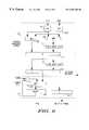
- FIG. 1 shows a block diagram of a correlator based demodulator 10 for M-level FSK signaling (M>1).
- the complex baseband signal (I & Q) is cross-correlated to M apriori known FSK signals. This is achieved by multiplying the received complex signal by the complex conjugates of the apriori known (or expected) signals at multipliers ( 12 ) and then integrating (or averaging) over a symbol period using a series of integrators 14 .
- the symbol corresponding to the correlator (CORR_i,i ⁇ M) with the maximum energy (or magnitude), detected over the specified period is chosen as the decoded symbol from among a series of correlators 16 .
- the desired symbol decision point is where the cross-correlation energy (or magnitude) is at its peak.
- An article entitled Coherent and Noncoherent Detection of CPFSK, by William P. Osborne and Michael B. Luntz, IEEE Transactions on Communications, Vol. COM-22, No. 8, August 1974, pp. 1023-1036 herein incorporated by reference provides further details on the theory of operation of the specified correlator based detector for M-level CPFSK signaling.
- the present invention preferably provides for a practical “multiplierless” implementation of a low cost and low power hardware architecture for an M-level correlation based FSK demodulator equivalent to what is shown in FIG. 1 .
- the reference to “multiplierless” essentially refers to the fact that the complex conjugate computations can be broken down into simple negation, zero, and pass through and the complex magnitude calculations can be broken down into shift and add/subtract operations.
- the parallel architecture shown in FIG. 1 can be implemented more cost efficiently in dedicated hardware by performing the computations in each of the correlator paths (or branches) in a serial manner. This is delineated in FIG. 2 .
- each pair of samples of I and Q arrive at the demodulator input of the demodulator 100 , they must be first multiplied by the complex conjugate of an apriori known signal, exp(jwkt) where k ⁇ M. This function is performed by a complex conjugate multiplier element 102 . The result must then be integrated over a desired integration window L, preferably using an integration filter 104 in the form of a boxcar filter coupled to the multiplier element. Next, the magnitude (or energy) of the specified correlator path must be computed so that it can be compared to the magnitudes from the other correlation paths, preferably achieved using a complex magnitude approximater element 106 coupled to the boxcar filter. The symbol corresponding to the correlation path with the highest magnitude over the indicated integration window is chosen as the detected symbol by a symbol generator element 108 or a maximum value and index holding element.
- FIG. 1 shows a parallel implementation which can be very costly
- the present invention is primarily directed to a serial architecture for a correlation based demodulator.
- the demodulator 100 of FIG. 2 essentially comprises a complex conjugate multiplier element 102 , an integration filter 104 , a complex magnitude approximater element 106 and a symbol generator 108 arranged and constructed in a serial fashion as shown.
- the multiplier element comprises hardware that reuses common products along an M-level of cross-correlation to reduce multiplication functions at a rate 2 ⁇ M times faster than a sampling rate (“X”) found at the demodulator input.
- the conjugate multiplier element 102 and the integration filter 104 operate on the I and Q signals independently for the M correlators at a rate of 2MX for the M correlators.
- the complex magnitude approximater element 106 and the symbol generator 108 both operate at a sampling rate of MX on the I and Q signal paths simultaneously to provide a single output from each of the respective elements.
- the boxcar filter used preferably integrates the results from the multiplier element over an L sample period by first differentiating and then integrating while the complex magnitude approximater element obtains an approximation of the complex magnitude at the boxcar filter output without using multiplier or square root elements.
- the symbol generator preferably uses a series of complex magnitude approximation outputs to generate symbols from two registers as will be more further detailed below.
- the demodulator input signal may be represented mathematically as:
- correlation_out (cos( w in t )+ j sin( w in t ))*(cos( w k t ) ⁇ j sin( w k t ))
- I 1 k cos( w in t )cos( w k t )+sin( w in t )sin( w k t )
- I 1 ⁇ k cos( w in t )cos( w k t ) ⁇ sin( w in t )sin( w k t )
- FIG. 3 further delineates the hardware architecture for the complex conjugate multiplier element 102 discussed.
- the present invention including the complex conjugate multiplier element is preferably implemented as a “multiplierless” demodulator. No multiplication functions are required, even for the complex conjugate multiplier element.
- the output of a simple counter is decoded to generate the 2-bit wide sin(w k t) (or Q k ) term.
- a 90 degree phase offset constant term is added to the counter output to generate the 2-bit wide cos(w k t) (or I k ) using the same decoding logic.
- Multiplication of the B-bit wide I and Q demodulator inputs by the 2-bit wide apriori signal (1,0, ⁇ 1) is achieved by simply performing either a pass through operation (i.e., multiply by 1), take the two's complement of the input signal (i.e., multiply by ⁇ 1), or zero out the input (i.e., multiply by 0).
- the complex conjugate multiplier element 102 is preferably a two's complement, pass-through, zero-out complex conjugate multiplier element.
- the equations above for I 1 k , Q 1 k , I 1 ⁇ k , and Q 1 ⁇ k show that only 4 multiplications are needed, results of which, are either added or subtracted appropriately. This is taken into account by the 3-stage tapped delay line 212 illustrated in FIG. 3 .
- the first three iterations through the datapath from the input to the MUX output can generate 3 of the 4 desired multiplication results.
- the complex conjugate multiplication results (I 1 , Q 1 ) must next be integrated over an L-sample period.
- An L-sample wide rectangular window filter (or boxcar filter of length L) is preferably used to integrate over the last L samples and then dump the result. This type of filter was observed to be the most efficient considering receiver performance under different RF conditions, cost, and current drain.
- a functional diagram of a boxcar filter 300 shown in FIG. 4 of length L is typically described as a digital integrator 302 followed by a differentiator 304 of length L. The latter simply subtracts out the integration result from L samples ago to implement a rectangular window of length L.
- the boxcar filter preferably receives an input at a differentiator and provides an output at an integrator.
- the differentiator 304 preferably comprises a counter 310 and a random access memory 320 having a height of 2 ⁇ M ⁇ L words and a width of B+2 bits, wherein M represents the number of FM levels, L represents the correlator integration window length, and B represent the number of bits originally received by the demodulator.
- the integrator 302 preferably comprises a counter 370 and a random access memory 380 having a height of 2 ⁇ M words and a width of B+2 bits+log 2 L bits.
- the integrator To support the largest possible values in a boxcar filter of length L, the integrator must support input bit width growth of log 2 L bits inside it. In other words, the internal bit width of the integrator must be log 2 L bits larger than its input bit width. However, in a traditional “integrator followed by a differentiator” boxcar filter, this causes the differentiator bit width to also be log 2 L bits larger. The latter is very undesirable from a cost and current drain perspective because it means that the differentiator needs to provide additional storage space for “2 ⁇ M ⁇ L ⁇ log2L” extra bits.
- the reasons for this include a “2 ⁇ M” factor which is the number of words of storage space needed for “2 ⁇ M” differentiators to support M-level FSK demodulation ( ⁇ M) for both the I and Q channels ( ⁇ 2).
- the factor L i.e., ⁇ L
- the factor “log 2 L”( ⁇ log 2 L) is the bit width growth that would otherwise be needed if the positions of the integrator and differentiator were not swapped. For these reasons, the differentiators 304 were placed in front of the integrators 302 to minimize cost and power drain.
- the differentiators 304 need only be the same bit width of the incoming I 1 and Q 1 data and allow the bit width growth to only occur in the latter integrator 302 .
- the savings of this scheme is “2 ⁇ M ⁇ L ⁇ log 2 L” bits of storage space which is significant from both a cost as well as a current drain perspective.
- the savings is 480 bits of storage space.
- Another optimization in the boxcar filter 104 includes the use of a RAM (Read-Access-Memory) ( 320 ) as opposed to using more costly and more power hungry flip-flops/latches to provide all the storage needs for the “2 ⁇ M” differentiators.
- a RAM Read-Access-Memory
- I 1 and Q 1 from the complex conjugate multiplication unit
- each sample is stored in a sequential fashion in the RAM. As this is performed on a cycle by cycle basis, previous contents of these RAM locations are read out during the same cycle to perform the length L differentiation for the operand supplied in that cycle.
- a simple counter 310 is used for this functionality as opposed to having to use twice the number of cycles because the read and write pointers have distinctly elaborate access mechanisms.
- the integrator hardware architecture ( 302 ) is also shown in FIG. 5 .
- the number of words of storage in the integrator 302 need only be “2 ⁇ M” deep since it only needs to store the results from 1 sample ago for both the I and the Q channels of the M correlators.
- This storage may be performed using either discrete registers or a custom RAM 380 depending upon the actual number of bits of storage needed (i.e., the actual size of “2 ⁇ M ⁇ (B+2+log2L)” bits). Similar to the differentiator memory, sequential addressing is also employed in the integrator to allow for simple counter based read/write addressing of the latter using the counter 370 .
- a clearing scheme is provided for both the differentiators and integrators using gates 330 and 360 respectively.
- These gates allow for the desired functionality in the boxcar filter when the order of the integrator and differentiator is swapped as herein.
- these gates serve as clearing elements at an output of a random access memory to allow for dynamic switching of a window length L. It is also desirable to clear both these units at periodic warm-up states as a fail-safe feature. There are several reasons for clearing. For one, due to some unlikely deterministic data pattern the integrator may get stuck at a large value and then never recover as a result of the switching of positions between the differentiator and the integrator.
- sensitivity and simulcast performance may be optimized by simply altering the integration window dynamically based upon the data rate received.
- both the integrator as well as the differentiator must be reset.
- the integrator must be reset because if window size X is changed to window size Y (where X>Y) without clearing it, the integrator will contain a DC component comprised of cross-correlation data from the previous X ⁇ Y samples that will never be cleared out. This would obviously cause erroneous results.
- the differentiators should also be cleared when performing a integration length change to avoid using data from more than a symbol ago in the situation in which the new window size is smaller than the previous one.
- the specified clearing scheme is performed by simply clearing the outputs of the integrator and differentiator RAMs rather than clearing each one of the RAM locations individually.
- One advantage of performing the clearing in this manner is obviously lower cost.
- Another advantage of clearing out the differentiator in this fashion is that when the integration length is dynamically changed from X to Y (where X>Y), the differentiator RAM will be already containing the desired data from Y samples ago immediately after the integration length change. Thus, the differentiator 304 will be immediately supplying correct data to the integrator 302 after such a window change without having to wait for the differentiator RAM ( 320 ) to fill up again. This results in a dynamic change of the integration window size without losing any incoming data samples.
- a combined complex magnitude approximater and symbol generator element 400 is shown having a complex magnitude approximater element 106 and a symbol generator 108 .
- the magnitude of the cross-correlation energy must next be computed. This may be computed as:
- FIG. 6 illustrates a hardware implementation of the indicated equation in a cost efficient manner. Note that the MAX and MIN blocks ( 406 and 408 respectively) in this diagram outputs the maximum and minimum of their operands, respectively. Also, the ABS block ( 402 and 404 ) generates the absolute value of the input operand. The computation of “max+min/2” of the absolute values of the input operands is quite straight forward as shown in FIG. 6 .
- the greater magnitude is stored in the “MAG(j)” register 420 .
- the symbol corresponding to the value stored in the MAG(j) register is loaded in to the “j” register 422 as shown in FIG. 6 .
- the symbol stored in the latter register at the end of each L sampling instance is the detected symbol (correlator number) for that instance.
- the output of the complex magnitude approximater element 106 can further be used for clock recovery.
- the output of block 416 can provide by the end of each symbol period information sufficient to determine the particular L sampling instance (or phase) for each of the M correlators to aide in clock recovery.
- the external clock recovery circuitry generates a pulse to capture the symbol corresponding to the maximum magnitude detected at the output of symbol generator ( 108 ).
- a rectangular window boxcar filter was preferably used as the integration filter as opposed to using more costly windowing schemes where M is the number of FSK levels and L is the integration length.
- the positions of the integrator and differentiator were swapped in the boxcar filter to localize the bit width growth in only the integrator and not in the differentiator.
- the cost and size savings here was “2 ⁇ M ⁇ L ⁇ log 2 L” bits.
- a resource shared RAM allowing for sequential addressing was used in the differentiators. Clearing of the differentiator and integrator was performed at the RAM outputs to minimize cost without losing any incoming data samples when the integration length was dynamically changed.
- a very low cost and low power approximation was used to perform the complex magnitude calculation without the need to use any multiplication or square root elements. Only 2 registers as opposed to “2 ⁇ N ⁇ M” registers were used in the symbol generation process where N is the number of samples in a symbol period and M is the number of FSK symbols.
Landscapes
- Physics & Mathematics (AREA)
- Spectroscopy & Molecular Physics (AREA)
- Engineering & Computer Science (AREA)
- Computer Networks & Wireless Communication (AREA)
- Signal Processing (AREA)
- Synchronisation In Digital Transmission Systems (AREA)
Abstract
Description

Claims (21)
Priority Applications (1)
| Application Number | Priority Date | Filing Date | Title |
|---|---|---|---|
| US09/285,977 US6487260B1 (en) | 1999-04-05 | 1999-04-05 | Method and apparatus for efficient correlation detection |
Applications Claiming Priority (1)
| Application Number | Priority Date | Filing Date | Title |
|---|---|---|---|
| US09/285,977 US6487260B1 (en) | 1999-04-05 | 1999-04-05 | Method and apparatus for efficient correlation detection |
Publications (1)
| Publication Number | Publication Date |
|---|---|
| US6487260B1 true US6487260B1 (en) | 2002-11-26 |
Family
ID=23096504
Family Applications (1)
| Application Number | Title | Priority Date | Filing Date |
|---|---|---|---|
| US09/285,977 Expired - Lifetime US6487260B1 (en) | 1999-04-05 | 1999-04-05 | Method and apparatus for efficient correlation detection |
Country Status (1)
| Country | Link |
|---|---|
| US (1) | US6487260B1 (en) |
Cited By (11)
| Publication number | Priority date | Publication date | Assignee | Title |
|---|---|---|---|---|
| US6707846B1 (en) * | 1999-07-12 | 2004-03-16 | Fujitsu Limited | Correlation energy detector and radio communication apparatus |
| US20050076072A1 (en) * | 2001-02-20 | 2005-04-07 | Masahiko Muto | Symbol points estimating device, method and program, recording medium on which the program is recorded, and modulation analyzing device |
| US6954483B2 (en) * | 1999-07-16 | 2005-10-11 | Infineon Technologies Ag | Method and device for synchronizing mobile radio receivers in a mobile radio system |
| US20070014384A1 (en) * | 2005-07-15 | 2007-01-18 | Samsung Electro-Mechanics Co., Ltd. | Multiple differential demodulator using weighting value |
| US20070036247A1 (en) * | 2005-08-12 | 2007-02-15 | Stmicroelectronics Belgium Nv | Receiver with frequency offset compensation for M-state phase modulation |
| US20070248195A1 (en) * | 2006-04-25 | 2007-10-25 | Texas Instruments Incorporated | Apparatus for and method of robust packet detection and frequency offset estimation |
| US20080008230A1 (en) * | 2006-07-10 | 2008-01-10 | Samsung Electro-Mechanics Co., Ltd. | Demodulator and demodulating method for WPAN |
| US20080101515A1 (en) * | 2005-01-07 | 2008-05-01 | Postdata Co., Ltd. | Device And Method For Detecting Symbol Timing For Highly Bandwidth Efficient High Order Modulation System |
| US20150341195A1 (en) * | 2012-11-28 | 2015-11-26 | Fraunhofer-Gesellschaft zur Förderung der angewandten Forschung e.V. | Device and method of sequence detection for frequency-shift keying |
| WO2019134947A3 (en) * | 2018-01-04 | 2020-01-09 | Nordic Semiconductor Asa | Matched-filter radio receiver |
| US11206170B2 (en) * | 2018-12-19 | 2021-12-21 | Nxp B.V. | Communications device and method for operating a communications device |
Citations (3)
| Publication number | Priority date | Publication date | Assignee | Title |
|---|---|---|---|---|
| US5287299A (en) * | 1992-05-26 | 1994-02-15 | Monolith Technologies Corporation | Method and apparatus for implementing a digital filter employing coefficients expressed as sums of 2 to an integer power |
| US5862068A (en) * | 1996-06-05 | 1999-01-19 | Sharp Kabushiki Kaisha | Arithmetic circuit for calculating a square-root of a sum of squares |
| US6263014B1 (en) * | 1998-09-03 | 2001-07-17 | Motorola, Inc. | Method and apparatus for correlation detection of multi-level signals with non-standard deviations |
-
1999
- 1999-04-05 US US09/285,977 patent/US6487260B1/en not_active Expired - Lifetime
Patent Citations (3)
| Publication number | Priority date | Publication date | Assignee | Title |
|---|---|---|---|---|
| US5287299A (en) * | 1992-05-26 | 1994-02-15 | Monolith Technologies Corporation | Method and apparatus for implementing a digital filter employing coefficients expressed as sums of 2 to an integer power |
| US5862068A (en) * | 1996-06-05 | 1999-01-19 | Sharp Kabushiki Kaisha | Arithmetic circuit for calculating a square-root of a sum of squares |
| US6263014B1 (en) * | 1998-09-03 | 2001-07-17 | Motorola, Inc. | Method and apparatus for correlation detection of multi-level signals with non-standard deviations |
Non-Patent Citations (4)
| Title |
|---|
| Benvenuto, Franks, and Hill, Dynamic Programming Methods for Designing FIR Filters Using Coefficients −1,0, and +1, IEEE, vol. ASSP-34, No. 4, Aug. 1986, pp. 785-792. |
| Benvenuto, Franks, and Hill, Dynamic Programming Methods for Designing FIR Filters Using Coefficients -1,0, and +1, IEEE, vol. ASSP-34, No. 4, Aug. 1986, pp. 785-792. |
| Chen, Koo and Wilson, A Simplified Signed Powers-of-Two Conversion for Multiplierless Adaptive Filters, IEEE, 1996 pp. 364-367. |
| Osborne and Luntz, Coherent and Noncoherent Detection of CPFSK, IEEE, vol. Com-22, No. 8, Aug. 1974, pp. 1023-1036. |
Cited By (19)
| Publication number | Priority date | Publication date | Assignee | Title |
|---|---|---|---|---|
| US6707846B1 (en) * | 1999-07-12 | 2004-03-16 | Fujitsu Limited | Correlation energy detector and radio communication apparatus |
| US6954483B2 (en) * | 1999-07-16 | 2005-10-11 | Infineon Technologies Ag | Method and device for synchronizing mobile radio receivers in a mobile radio system |
| US20050076072A1 (en) * | 2001-02-20 | 2005-04-07 | Masahiko Muto | Symbol points estimating device, method and program, recording medium on which the program is recorded, and modulation analyzing device |
| US20080101515A1 (en) * | 2005-01-07 | 2008-05-01 | Postdata Co., Ltd. | Device And Method For Detecting Symbol Timing For Highly Bandwidth Efficient High Order Modulation System |
| US20070014384A1 (en) * | 2005-07-15 | 2007-01-18 | Samsung Electro-Mechanics Co., Ltd. | Multiple differential demodulator using weighting value |
| US7643579B2 (en) * | 2005-07-15 | 2010-01-05 | Samsung Electro-Mechanics Co., Ltd. | Multiple differential demodulator using weighting value |
| US20070036247A1 (en) * | 2005-08-12 | 2007-02-15 | Stmicroelectronics Belgium Nv | Receiver with frequency offset compensation for M-state phase modulation |
| US8155250B2 (en) * | 2005-08-12 | 2012-04-10 | St-Ericsson Sa | Receiver with frequency offset compensation for M-state phase modulation |
| US20070248195A1 (en) * | 2006-04-25 | 2007-10-25 | Texas Instruments Incorporated | Apparatus for and method of robust packet detection and frequency offset estimation |
| US9184971B2 (en) * | 2006-04-25 | 2015-11-10 | Texas Instruments Incorporated | Apparatus for and method of robust packet detection and frequency offset estimation |
| US20080008230A1 (en) * | 2006-07-10 | 2008-01-10 | Samsung Electro-Mechanics Co., Ltd. | Demodulator and demodulating method for WPAN |
| US7756195B2 (en) * | 2006-07-10 | 2010-07-13 | Samsung Electro-Mechanics Co., Ltd. | Demodulator and demodulating method for WPAN |
| US20150341195A1 (en) * | 2012-11-28 | 2015-11-26 | Fraunhofer-Gesellschaft zur Förderung der angewandten Forschung e.V. | Device and method of sequence detection for frequency-shift keying |
| US9450793B2 (en) * | 2012-11-28 | 2016-09-20 | Fraunhofer-Gesellschaft Zur Foerderung Der Angewandten Forschung E.V. | Device and method of sequence detection for frequency-shift keying |
| WO2019134947A3 (en) * | 2018-01-04 | 2020-01-09 | Nordic Semiconductor Asa | Matched-filter radio receiver |
| CN111684729A (en) * | 2018-01-04 | 2020-09-18 | 北欧半导体公司 | Matched filter radio receiver |
| US11228471B2 (en) * | 2018-01-04 | 2022-01-18 | Nordic Semiconductor Asa | Matched-filter radio receiver |
| CN111684729B (en) * | 2018-01-04 | 2022-06-24 | 北欧半导体公司 | Matched filter radio receiver |
| US11206170B2 (en) * | 2018-12-19 | 2021-12-21 | Nxp B.V. | Communications device and method for operating a communications device |
Similar Documents
| Publication | Publication Date | Title |
|---|---|---|
| EP1913747B1 (en) | Fast carrier frequency error estimation algorithm using sychronization sequence | |
| US8774318B2 (en) | Method and apparatus for constant envelope modulation | |
| US6055281A (en) | Passband DQPSK detector for a digital communications receiver | |
| US8761230B2 (en) | Method and apparatus for continuous phase modulation preamble encoding and decoding | |
| FI113228B (en) | Quantified coherent RAKE receiver | |
| US6487260B1 (en) | Method and apparatus for efficient correlation detection | |
| US5748680A (en) | Coarse frequency burst detector for a wireline communications system | |
| CN101490660A (en) | Improved precision CORDIC processor | |
| US7099410B1 (en) | Reduced complexity MLSE equalizer for M-ary modulated signals | |
| CN107888230B (en) | Multiphase coherent integration acquisition method applied to weak signal environment | |
| US6973142B2 (en) | Timing synchronization for M-DPSK channels | |
| CN103439718A (en) | Unambiguous tracking unit of high-order BOC modulation signals | |
| JPH07273702A (en) | Receiver receiving signal consisting of symbol array and equalizer therefor and symbol detecting method | |
| US5786725A (en) | Reduced complexity maximum likelihood multiple symbol differential detector | |
| US6873666B2 (en) | Circuit and method for symbol timing recovery in phase modulation systems | |
| EP0717512A2 (en) | Coarse frequency burst detector for a wireless communications systems, such as for use with GSM | |
| US7302016B1 (en) | Phase estimator with bias correction | |
| US6594324B1 (en) | Correlation operation method and matched filter | |
| US5592514A (en) | Method of performing signal reconstruction at the receiving end of a communications system, such as for GSM | |
| CN107846262B (en) | Demodulation code rate detection method based on differential correlation operation | |
| JP3839569B2 (en) | Unique word detection method | |
| JP4970283B2 (en) | High memory efficiency sliding window addition | |
| US7395291B2 (en) | Multiplierless correlators for HIPERLAN/2 and IEEE 802.11A wireless local area networks | |
| US6940927B2 (en) | Simplified symbol timing tracking circuit for a CPM modulated signal | |
| JPH1117652A (en) | Frame synchronization detection circuit |
Legal Events
| Date | Code | Title | Description |
|---|---|---|---|
| AS | Assignment |
Owner name: MOTOROLA, INC., ILLINOIS Free format text: ASSIGNMENT OF ASSIGNORS INTEREST;ASSIGNORS:SCHWEICKERT, ROBERT K.;RAHMAN, MAHIBUR;THOMAS, CHRISTOPHER T.;AND OTHERS;REEL/FRAME:009879/0579 Effective date: 19990329 |
|
| STCF | Information on status: patent grant |
Free format text: PATENTED CASE |
|
| AS | Assignment |
Owner name: FREESCALE SEMICONDUCTOR, INC., TEXAS Free format text: ASSIGNMENT OF ASSIGNORS INTEREST;ASSIGNOR:MOTOROLA, INC.;REEL/FRAME:015603/0258 Effective date: 20041210 |
|
| FPAY | Fee payment |
Year of fee payment: 4 |
|
| AS | Assignment |
Owner name: CITIBANK, N.A. AS COLLATERAL AGENT, NEW YORK Free format text: SECURITY AGREEMENT;ASSIGNORS:FREESCALE SEMICONDUCTOR, INC.;FREESCALE ACQUISITION CORPORATION;FREESCALE ACQUISITION HOLDINGS CORP.;AND OTHERS;REEL/FRAME:018855/0129 Effective date: 20061201 Owner name: CITIBANK, N.A. AS COLLATERAL AGENT,NEW YORK Free format text: SECURITY AGREEMENT;ASSIGNORS:FREESCALE SEMICONDUCTOR, INC.;FREESCALE ACQUISITION CORPORATION;FREESCALE ACQUISITION HOLDINGS CORP.;AND OTHERS;REEL/FRAME:018855/0129 Effective date: 20061201 |
|
| FPAY | Fee payment |
Year of fee payment: 8 |
|
| AS | Assignment |
Owner name: CITIBANK, N.A., AS COLLATERAL AGENT,NEW YORK Free format text: SECURITY AGREEMENT;ASSIGNOR:FREESCALE SEMICONDUCTOR, INC.;REEL/FRAME:024397/0001 Effective date: 20100413 Owner name: CITIBANK, N.A., AS COLLATERAL AGENT, NEW YORK Free format text: SECURITY AGREEMENT;ASSIGNOR:FREESCALE SEMICONDUCTOR, INC.;REEL/FRAME:024397/0001 Effective date: 20100413 |
|
| AS | Assignment |
Owner name: APPLE INC., CALIFORNIA Free format text: ASSIGNMENT OF ASSIGNORS INTEREST;ASSIGNOR:FREESCALE SEMICONDUCTOR, INC.;REEL/FRAME:026304/0200 Effective date: 20110411 |
|
| FPAY | Fee payment |
Year of fee payment: 12 |
|
| AS | Assignment |
Owner name: FREESCALE SEMICONDUCTOR, INC., TEXAS Free format text: PATENT RELEASE;ASSIGNOR:CITIBANK, N.A., AS COLLATERAL AGENT;REEL/FRAME:037356/0143 Effective date: 20151207 Owner name: FREESCALE SEMICONDUCTOR, INC., TEXAS Free format text: PATENT RELEASE;ASSIGNOR:CITIBANK, N.A., AS COLLATERAL AGENT;REEL/FRAME:037354/0225 Effective date: 20151207 Owner name: FREESCALE SEMICONDUCTOR, INC., TEXAS Free format text: PATENT RELEASE;ASSIGNOR:CITIBANK, N.A., AS COLLATERAL AGENT;REEL/FRAME:037356/0553 Effective date: 20151207 |