US6469699B2 - Sample hold circuit - Google Patents

Sample hold circuit Download PDF

Info

Publication number
US6469699B2
US6469699B2 US09/097,391 US9739198A US6469699B2 US 6469699 B2 US6469699 B2 US 6469699B2 US 9739198 A US9739198 A US 9739198A US 6469699 B2 US6469699 B2 US 6469699B2
Authority
US
United States
Prior art keywords
sample
master clock
hold
circuit
common substrate
Prior art date
Legal status (The legal status is an assumption and is not a legal conclusion. Google has not performed a legal analysis and makes no representation as to the accuracy of the status listed.)
Expired - Lifetime
Application number
US09/097,391
Other versions
US20010043186A1 (en
Inventor
Hiroyuki Yoshine
Current Assignee (The listed assignees may be inaccurate. Google has not performed a legal analysis and makes no representation or warranty as to the accuracy of the list.)
Sony Corp
Original Assignee
Sony Corp
Priority date (The priority date is an assumption and is not a legal conclusion. Google has not performed a legal analysis and makes no representation as to the accuracy of the date listed.)
Filing date
Publication date
Application filed by Sony Corp filed Critical Sony Corp
Assigned to SONY CORPORATION reassignment SONY CORPORATION ASSIGNMENT OF ASSIGNORS INTEREST (SEE DOCUMENT FOR DETAILS). Assignors: YOSHINE, HIROYUKI
Publication of US20010043186A1 publication Critical patent/US20010043186A1/en
Application granted granted Critical
Publication of US6469699B2 publication Critical patent/US6469699B2/en
Anticipated expiration legal-status Critical
Expired - Lifetime legal-status Critical Current

Links

Images

Classifications

    • GPHYSICS
    • G09EDUCATION; CRYPTOGRAPHY; DISPLAY; ADVERTISING; SEALS
    • G09GARRANGEMENTS OR CIRCUITS FOR CONTROL OF INDICATING DEVICES USING STATIC MEANS TO PRESENT VARIABLE INFORMATION
    • G09G3/00Control arrangements or circuits, of interest only in connection with visual indicators other than cathode-ray tubes
    • G09G3/20Control arrangements or circuits, of interest only in connection with visual indicators other than cathode-ray tubes for presentation of an assembly of a number of characters, e.g. a page, by composing the assembly by combination of individual elements arranged in a matrix no fixed position being assigned to or needed to be assigned to the individual characters or partial characters
    • GPHYSICS
    • G09EDUCATION; CRYPTOGRAPHY; DISPLAY; ADVERTISING; SEALS
    • G09GARRANGEMENTS OR CIRCUITS FOR CONTROL OF INDICATING DEVICES USING STATIC MEANS TO PRESENT VARIABLE INFORMATION
    • G09G5/00Control arrangements or circuits for visual indicators common to cathode-ray tube indicators and other visual indicators
    • G09G5/003Details of a display terminal, the details relating to the control arrangement of the display terminal and to the interfaces thereto
    • G09G5/006Details of the interface to the display terminal
    • G09G5/008Clock recovery
    • GPHYSICS
    • G09EDUCATION; CRYPTOGRAPHY; DISPLAY; ADVERTISING; SEALS
    • G09GARRANGEMENTS OR CIRCUITS FOR CONTROL OF INDICATING DEVICES USING STATIC MEANS TO PRESENT VARIABLE INFORMATION
    • G09G2310/00Command of the display device
    • G09G2310/08Details of timing specific for flat panels, other than clock recovery
    • GPHYSICS
    • G09EDUCATION; CRYPTOGRAPHY; DISPLAY; ADVERTISING; SEALS
    • G09GARRANGEMENTS OR CIRCUITS FOR CONTROL OF INDICATING DEVICES USING STATIC MEANS TO PRESENT VARIABLE INFORMATION
    • G09G2330/00Aspects of power supply; Aspects of display protection and defect management
    • G09G2330/06Handling electromagnetic interferences [EMI], covering emitted as well as received electromagnetic radiation
    • GPHYSICS
    • G09EDUCATION; CRYPTOGRAPHY; DISPLAY; ADVERTISING; SEALS
    • G09GARRANGEMENTS OR CIRCUITS FOR CONTROL OF INDICATING DEVICES USING STATIC MEANS TO PRESENT VARIABLE INFORMATION
    • G09G2352/00Parallel handling of streams of display data
    • GPHYSICS
    • G09EDUCATION; CRYPTOGRAPHY; DISPLAY; ADVERTISING; SEALS
    • G09GARRANGEMENTS OR CIRCUITS FOR CONTROL OF INDICATING DEVICES USING STATIC MEANS TO PRESENT VARIABLE INFORMATION
    • G09G3/00Control arrangements or circuits, of interest only in connection with visual indicators other than cathode-ray tubes
    • G09G3/20Control arrangements or circuits, of interest only in connection with visual indicators other than cathode-ray tubes for presentation of an assembly of a number of characters, e.g. a page, by composing the assembly by combination of individual elements arranged in a matrix no fixed position being assigned to or needed to be assigned to the individual characters or partial characters
    • G09G3/34Control arrangements or circuits, of interest only in connection with visual indicators other than cathode-ray tubes for presentation of an assembly of a number of characters, e.g. a page, by composing the assembly by combination of individual elements arranged in a matrix no fixed position being assigned to or needed to be assigned to the individual characters or partial characters by control of light from an independent source
    • G09G3/36Control arrangements or circuits, of interest only in connection with visual indicators other than cathode-ray tubes for presentation of an assembly of a number of characters, e.g. a page, by composing the assembly by combination of individual elements arranged in a matrix no fixed position being assigned to or needed to be assigned to the individual characters or partial characters by control of light from an independent source using liquid crystals
    • G09G3/3611Control of matrices with row and column drivers

Definitions

  • This invention relates to a sample and hold circuit for sample-holding a video signal based on a master clock, and more particularly to a sample and hold circuit to use suitably for a horizontal driving system of a liquid crystal display device.
  • Some liquid crystal display (LCD) devices have the structure in which a video signal is simultaneously inputted using multi-channels in order to reduce driving frequency of an LCD panel.
  • a sample hold circuit for sampling simultaneously multi-bits (pixels) corresponding to the number of channels is used in order to input a video signal using multi-channels.
  • the sample and hold circuit 100 comprises a inversion amplifier 101 for inverting an input video signal, six sample hold units (SH 1 to SH 6 ) 102 to 107 corresponding to 6 channels which receive an output signal from the inversion amplifier 101 , and SHP generation circuit 108 for generating 6 types of sample hold pulses SHP 1 to SHP 6 corresponding to six sample hold units 102 to 107 based on a master clock MCLK given from the outside, and the sample and hold circuit 100 is IC (Integrated Circuit) structured.
  • IC Integrated Circuit
  • a PLL (Phase-Locked Loop) circuit 110 for supplying a master clock MCLK is provided to the sample and hold circuit 100 as an external circuit.
  • the PLL circuit 110 generates a master clock MCLK synchronously to a horizontal sync signal HSYNC namely a comparison reference signal.
  • the master clock MCLK is oscillated at a frequency 12 times that of the horizontal clock HCK which is used as a reference of horizontal scanning of the LCD.
  • the conventional sample and hold circuit used for a horizontal driving system of a 6-dot simultaneous sampling liquid crystal display device has the structure in which the master clock MCLK is transmitted from a PLL circuit 110 provided as a separate external circuit to the sample and hold circuit, the structure is inevitably provided with wiring for transmitting the master clock MCLK to an external substrate, and in an exemplary 6-dot simultaneous sampling, because frequency of the master clock MCLK is 12 times that of the horizontal clock HCK, the high frequency causes a problem of unwanted radiation. To reduce the unwanted radiation, additional parts dedicated for reduction of the unwanted radiation are required, and the number of parts of the circuit increases resulting in increased cost.
  • the present invention is accomplished in view of the above-mentioned problem, it is the object of the present invention to provide a sample and hold circuit with reduced unwanted radiation which does not require complex wiring for transmitting the master clock MCLK.
  • a sample and hold circuit in accordance with the present invention is a sample and hold circuit for sample-holding a video signal based on a master clock, and has the structure having a PLL circuit for generating a master clock synchronously to a comparison reference signal supplied from the external provided on the common substrate.
  • the structure that the PLL circuit is provided on the common substrate and contained in the common IC allows the complex wiring to the external substrate for transmitting the master clock generated by the PLL circuit to be eliminated. Unwanted radiation due to complex wiring is reduced and need for parts to prevent unwanted radiation is eliminated in spite of high frequency of the master clock.
  • FIG. 1 is a block diagram for illustrating an embodiment of the present invention.
  • FIG. 2 is a timing chart for showing the timing relation between the sample hold pulse SHP and master clock MCLK.
  • FIG. 3 is a block diagram for illustrating an exemplary circuit structure of a PLL circuit.
  • FIG. 4 is a timing chart for describing the timing control concept of the horizontal start pulse HST.
  • FIG. 5 is a block diagram for illustrating a conventional example.
  • FIG. 1 is a block diagram f or illustrating a sample and hold circuit in accordance with the present invention used, for example, for a horizontal driving system of a 6-dot simultaneous sampling liquid crystal display device.
  • the sample and hold circuit 10 in accordance with the present invention has the structure provided with an inversion amplifier 11 , six sample and hold units (SH 1 to SH 6 ) 12 to 17 , and an SHP generation circuit 18 , and has a PLL circuit 19 on the common substrate (chip) (built-in).
  • the sample and hold circuit 10 has an IC structure.
  • the inversion amplifier 11 inverts an input video signal, and inputs it to six sample hold units 12 to 17 corresponding to 6 channels.
  • the sample and hold circuit 10 supplies the sample-held video signal to a liquid crystal panel 500 based on the sample and hold pulses SH 1 to SH 6 .
  • a video signal having the phase adjusted with respect to the horizontal sync signal is supplied to the liquid crystal panel 500 through 6 signal lines.
  • the SHP generation circuit 18 generates successively 6 types of sample and hold pulses SHP 1 to SHP 6 corresponding to 6 sample hold units 12 to 17 for every one clock of the master clock MCLK generated by the PLL circuit 19 as shown in the timing chart of FIG. 2 . As the result, the phase of sample hold pulses SHP 1 to SHP 6 is shifted successively by a period of the master clock MCLK.
  • the PLL circuit 19 generates the master clock MCLK to be supplied to the SHP generation circuit 18 based on the horizontal sync signal HSYNC namely the comparison reference signal provided externally.
  • the PLL circuit 19 comprises a phase comparison circuit 21 which uses the horizontal sync signal HSYNC as the comparison reference signal, a LPF (Low Pass Filter) 22 for removing AC component of comparison output of the phase comparison circuit 21 , a VCO (Voltage Control Oscillator) 23 which uses DC voltage supplied form the LPF 22 as the control voltage, a frequency divider 24 for dividing the oscillation output of the VCO 23 into 12 , and a frequency divider 25 for dividing the frequency divided output from the frequency divider 24 into 88 namely the frequency of the horizontal sync signal HXYNC and supplying it to the phase comparison circuit 20 .
  • a phase comparison circuit 21 which uses the horizontal sync signal HSYNC as the comparison reference signal
  • VCO Voltage Control Oscillator
  • the oscillation output of the VCO 23 is outputted as the master clock MCLK to be supplied to the SHP generation circuit 18 .
  • the frequency divided output of the frequency divider 24 is outputted as the horizontal clock HCK which is ⁇ fraction (1/12) ⁇ the frequency of the master clock MCLK.
  • the horizontal clock HCK is used as the scanning timing reference in the horizontal scanning system of the LCD.
  • the frequency divided output of the frequency divider 25 is outputted as the horizontal start pulse HST having a frequency equal to that of the horizontal sync signal HSYNC.
  • the horizontal start pulse HST is used as a reference to determine the position in the right-left direction (horizontal direction) on a picture displayed on the LCD.
  • the PLL circuit 19 has phase adjusting function to adjust arbitrarily the master clock MCLK with respect to the horizontal sync signal HSYNC.
  • the adjusting voltage Vc is added to the DC output voltage of the LPF 22 in the PLL circuit 19 , and the added voltage is supplied to the VCO 23 as a control voltage to perform phase adjustment of the master clock MCLK with respect to the horizontal sync signal HSYNC.
  • phase of the master clock MCLK is adjusted so as to be optimal for each device.
  • the sample and hold circuit 10 is provided with a built-in timing control circuit 20 for controlling the timing of the horizontal start pulse HST synchronously to the horizontal clock HCK.
  • the timing control circuit 20 functions to put the horizontal pulse HST outputted from the PLL circuit 19 ahead or back on the time axis by the number of clocks corresponding to the position adjusting information with reference to the horizontal clock HCK as shown in the timing chart of FIG. 4 .
  • the horizontal start pulse HST is the reference to determine the picture position in the horizontal direction on the LCD as described hereinbefore, by providing the built-in timing control circuit 20 for controlling the timing of the horizontal start pulse HST and by setting arbitrarily the position adjusting information provided externally, the sample hold circuit 10 is allowed to have the function for adjusting arbitrarily the position in the horizontal direction of the displayed picture on the LCD. As the result, the position of the displayed picture can be set arbitrarily.
  • the built-in PLL circuit 19 for generating the master clock MCLK on the IC-structured sample hold circuit 10 in a LCD for, for example, 6-dot simultaneous sampling of a video signal complex line wiring to the external substrate for transmitting the master clock MCLK to the sample and hold circuit 10 is unnecessary unlike the conventional art, in which the PLL circuit is provided externally.
  • Unwanted radiation due to complex wiring is reduced regardless of high frequency of the master clock.
  • the frequency of the master clock MCLK is 12 time that of the horizontal clock HCK, and for the liquid crystal display device of 12 dot simultaneous sampling, the master clock MCLK having a very high frequency 24 times that of the horizontal clock HCK is required, in such case the present invention is very effective for preventing unwanted radiation.
  • the built-in PLL circuit 19 prevents unwanted radiation, parts dedicated to prevent unwanted radiation can be eliminated, and the elimination contributes to reduce the cost. Further, wiring lines to transmit the master clock MCLK are eliminated, so the space for the wiring is unnecessary, and the area size of the external substrate is reduced.
  • the above-mentioned embodiment involves application of the present invention to a 6-dot simultaneous sampling liquid crystal display device, however, the present invention is by no means limited to the case, but is applied to a 12 dot simultaneous sampling liquid crystal display device similarly.

Landscapes

  • Engineering & Computer Science (AREA)
  • Physics & Mathematics (AREA)
  • Computer Hardware Design (AREA)
  • General Physics & Mathematics (AREA)
  • Theoretical Computer Science (AREA)
  • Liquid Crystal Display Device Control (AREA)

Abstract

In a horizontal driving system of a liquid crystal display, the high frequency of a master clock MCLK and complex wiring to an external substrate for transmitting the master clock MCLK cause disadvantageous unwanted radiation. A sample and hold circuit for sampling and holding a video signal based on the master clock MCLK is provided with a built-in PLL circuit for generating the master clock MCLK in order to eliminate complex wiring for transmitting the master clock MCLK and to reduce unwanted radiation.

Description

BACKGROUND OF THE INVENTION
1. Field of the Invention
This invention relates to a sample and hold circuit for sample-holding a video signal based on a master clock, and more particularly to a sample and hold circuit to use suitably for a horizontal driving system of a liquid crystal display device.
2. Description of Related Art
Some liquid crystal display (LCD) devices have the structure in which a video signal is simultaneously inputted using multi-channels in order to reduce driving frequency of an LCD panel. In a horizontal driving system of liquid crystal display devices of this sort, a sample hold circuit for sampling simultaneously multi-bits (pixels) corresponding to the number of channels is used in order to input a video signal using multi-channels.
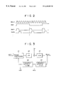
A conventional example of a sample and hold circuit used for a horizontal driving system of a liquid crystal display device of 6-dot simultaneous sampling is shown in FIG. 5. In this drawing, the sample and hold circuit 100 comprises a inversion amplifier 101 for inverting an input video signal, six sample hold units (SH1 to SH6) 102 to 107 corresponding to 6 channels which receive an output signal from the inversion amplifier 101, and SHP generation circuit 108 for generating 6 types of sample hold pulses SHP1 to SHP6 corresponding to six sample hold units 102 to 107 based on a master clock MCLK given from the outside, and the sample and hold circuit 100 is IC (Integrated Circuit) structured.
A PLL (Phase-Locked Loop) circuit 110 for supplying a master clock MCLK is provided to the sample and hold circuit 100 as an external circuit. The PLL circuit 110 generates a master clock MCLK synchronously to a horizontal sync signal HSYNC namely a comparison reference signal. For 6-dot simultaneous sampling, the master clock MCLK is oscillated at a frequency 12 times that of the horizontal clock HCK which is used as a reference of horizontal scanning of the LCD.
Because, for example, the conventional sample and hold circuit used for a horizontal driving system of a 6-dot simultaneous sampling liquid crystal display device has the structure in which the master clock MCLK is transmitted from a PLL circuit 110 provided as a separate external circuit to the sample and hold circuit, the structure is inevitably provided with wiring for transmitting the master clock MCLK to an external substrate, and in an exemplary 6-dot simultaneous sampling, because frequency of the master clock MCLK is 12 times that of the horizontal clock HCK, the high frequency causes a problem of unwanted radiation. To reduce the unwanted radiation, additional parts dedicated for reduction of the unwanted radiation are required, and the number of parts of the circuit increases resulting in increased cost.
The present invention is accomplished in view of the above-mentioned problem, it is the object of the present invention to provide a sample and hold circuit with reduced unwanted radiation which does not require complex wiring for transmitting the master clock MCLK.
SUMMARY OF THE INVENTION
A sample and hold circuit in accordance with the present invention is a sample and hold circuit for sample-holding a video signal based on a master clock, and has the structure having a PLL circuit for generating a master clock synchronously to a comparison reference signal supplied from the external provided on the common substrate.
In the sample and hold circuit having the above-mentioned structure, the structure that the PLL circuit is provided on the common substrate and contained in the common IC allows the complex wiring to the external substrate for transmitting the master clock generated by the PLL circuit to be eliminated. Unwanted radiation due to complex wiring is reduced and need for parts to prevent unwanted radiation is eliminated in spite of high frequency of the master clock.
BRIEF DESCRIPTION OF THE DRAWINGS
FIG. 1 is a block diagram for illustrating an embodiment of the present invention.
FIG. 2 is a timing chart for showing the timing relation between the sample hold pulse SHP and master clock MCLK.
FIG. 3 is a block diagram for illustrating an exemplary circuit structure of a PLL circuit.
FIG. 4 is a timing chart for describing the timing control concept of the horizontal start pulse HST.
FIG. 5 is a block diagram for illustrating a conventional example.
DETAILED DESCRIPTION OF THE PREFERRED EMBODIMENTS
Embodiments of the present invention will be described in detail hereinafter with reference to the drawings. FIG. 1 is a block diagram f or illustrating a sample and hold circuit in accordance with the present invention used, for example, for a horizontal driving system of a 6-dot simultaneous sampling liquid crystal display device.
In FIG. 1, the sample and hold circuit 10 in accordance with the present invention has the structure provided with an inversion amplifier 11, six sample and hold units (SH1 to SH6) 12 to 17, and an SHP generation circuit 18, and has a PLL circuit 19 on the common substrate (chip) (built-in). The sample and hold circuit 10 has an IC structure. In the sample and hold circuit 10, the inversion amplifier 11 inverts an input video signal, and inputs it to six sample hold units 12 to 17 corresponding to 6 channels. The sample and hold circuit 10 supplies the sample-held video signal to a liquid crystal panel 500 based on the sample and hold pulses SH1 to SH6. A video signal having the phase adjusted with respect to the horizontal sync signal is supplied to the liquid crystal panel 500 through 6 signal lines.
The SHP generation circuit 18 generates successively 6 types of sample and hold pulses SHP1 to SHP6 corresponding to 6 sample hold units 12 to 17 for every one clock of the master clock MCLK generated by the PLL circuit 19 as shown in the timing chart of FIG. 2. As the result, the phase of sample hold pulses SHP1 to SHP6 is shifted successively by a period of the master clock MCLK. The PLL circuit 19 generates the master clock MCLK to be supplied to the SHP generation circuit 18 based on the horizontal sync signal HSYNC namely the comparison reference signal provided externally.
One example of the circuit structure of the PLL circuit 19 is shown in FIG. 3. As shown in the drawing, the PLL circuit 19 comprises a phase comparison circuit 21 which uses the horizontal sync signal HSYNC as the comparison reference signal, a LPF (Low Pass Filter) 22 for removing AC component of comparison output of the phase comparison circuit 21, a VCO (Voltage Control Oscillator) 23 which uses DC voltage supplied form the LPF 22 as the control voltage, a frequency divider 24 for dividing the oscillation output of the VCO 23 into 12, and a frequency divider 25 for dividing the frequency divided output from the frequency divider 24 into 88 namely the frequency of the horizontal sync signal HXYNC and supplying it to the phase comparison circuit 20.
In the PLL circuit 19, the oscillation output of the VCO 23 is outputted as the master clock MCLK to be supplied to the SHP generation circuit 18. The frequency divided output of the frequency divider 24 is outputted as the horizontal clock HCK which is {fraction (1/12)}the frequency of the master clock MCLK. The horizontal clock HCK is used as the scanning timing reference in the horizontal scanning system of the LCD. The frequency divided output of the frequency divider 25 is outputted as the horizontal start pulse HST having a frequency equal to that of the horizontal sync signal HSYNC. The horizontal start pulse HST is used as a reference to determine the position in the right-left direction (horizontal direction) on a picture displayed on the LCD.
The PLL circuit 19 has phase adjusting function to adjust arbitrarily the master clock MCLK with respect to the horizontal sync signal HSYNC. In detail, when an adjusting voltage Vc corresponding to phase adjusting information is provided externally, the adjusting voltage Vc is added to the DC output voltage of the LPF 22 in the PLL circuit 19, and the added voltage is supplied to the VCO 23 as a control voltage to perform phase adjustment of the master clock MCLK with respect to the horizontal sync signal HSYNC. As the result, phase of the master clock MCLK is adjusted so as to be optimal for each device.
The sample and hold circuit 10 is provided with a built-in timing control circuit 20 for controlling the timing of the horizontal start pulse HST synchronously to the horizontal clock HCK. The timing control circuit 20 functions to put the horizontal pulse HST outputted from the PLL circuit 19 ahead or back on the time axis by the number of clocks corresponding to the position adjusting information with reference to the horizontal clock HCK as shown in the timing chart of FIG. 4.
Because the horizontal start pulse HST is the reference to determine the picture position in the horizontal direction on the LCD as described hereinbefore, by providing the built-in timing control circuit 20 for controlling the timing of the horizontal start pulse HST and by setting arbitrarily the position adjusting information provided externally, the sample hold circuit 10 is allowed to have the function for adjusting arbitrarily the position in the horizontal direction of the displayed picture on the LCD. As the result, the position of the displayed picture can be set arbitrarily.
As described herein above, by providing the built-in PLL circuit 19 for generating the master clock MCLK on the IC-structured sample hold circuit 10 in a LCD for, for example, 6-dot simultaneous sampling of a video signal, complex line wiring to the external substrate for transmitting the master clock MCLK to the sample and hold circuit 10 is unnecessary unlike the conventional art, in which the PLL circuit is provided externally.
Unwanted radiation due to complex wiring is reduced regardless of high frequency of the master clock. In this embodiment, application of the present invention to a horizontal driving system of a liquid crystal display device of 6-dot simultaneous sampling is assumed, the frequency of the master clock MCLK is 12 time that of the horizontal clock HCK, and for the liquid crystal display device of 12 dot simultaneous sampling, the master clock MCLK having a very high frequency 24 times that of the horizontal clock HCK is required, in such case the present invention is very effective for preventing unwanted radiation.
Because the built-in PLL circuit 19 prevents unwanted radiation, parts dedicated to prevent unwanted radiation can be eliminated, and the elimination contributes to reduce the cost. Further, wiring lines to transmit the master clock MCLK are eliminated, so the space for the wiring is unnecessary, and the area size of the external substrate is reduced.
The above-mentioned embodiment involves application of the present invention to a 6-dot simultaneous sampling liquid crystal display device, however, the present invention is by no means limited to the case, but is applied to a 12 dot simultaneous sampling liquid crystal display device similarly.
As described hereinbefore, according to the present invention, in a sample and hold circuit for sample holding of a video signal based on the master clock, because a built-in PLL circuit for generating the master clock is provided, complex wiring for transmitting the master clock to an external substrate is unnecessary, and unwanted radiation due to complex wiring is reduced.

Claims (6)

What is claimed is:
1. A sample and hold circuit comprising:
a common substrate;
a sample and hold pulse generation circuit formed on said common substrate for generating a plurality of sample and hold pulses for sampling and holding a video signal, wherein a phase of said plurality of sample and hold pulses is shifted successively by a period of a master clock;
a PLL circuit for generating said master clock in synchronism with a comparison reference signal provided externally and for generating a horizontal start pulse for use as a reference to determine a horizontal position of a displayed picture based on said video signal by dividing said master clock, wherein said PLL circuit is formed on said common substrate so that unwanted radiation is reduced regardless of a high frequency of said master clock; and
a plurality of sample and hold units formed on said common substrate and having as inputs said video signal and said plurality of sample and hold pulses.
2. The sample and hold circuit as claimed in claim 1, wherein said PLL circuit adjusts a phase of said master clock based on an externally provided signal.
3. The sample and hold circuit as claimed in claim 1, further comprising means for controlling the timing of said horizontal start pulse based on said externally provided signal.
4. A liquid crystal display device comprising:
a sample and hold circuit including:
a common substrate,
a sample and hold pulse generation circuit formed on said common substrate for generating a plurality of sample and hold pulses for sampling and holding a video signal, wherein a phase of said plurality of sample and hold pulses is shifted successively by a period of a master clock,
a PLL circuit for generating said master clock in synchronism with a comparison reference signal provided externally and for generating a horizontal start pulse for use as a reference to determine a horizontal position of a displayed picture based on said video signal by dividing said master clock, wherein said PLL circuit is formed on said common substrate so that unwanted radiation is reduced regardless of a high frequency of said master clock;
a plurality of sample and hold units formed on said common substrate and having as inputs said video signal and said plurality of sample and hold pulses; and
a liquid crystal panel for displaying an output from said plurality of sample and hold units.
5. The liquid crystal display device as claimed in claim 4, wherein said PLL circuit adjusts a phase of said master clock based on an externally provided signal.
6. The liquid crystal display device as claimed in claim 4, further comprising means for controlling the timing of said horizontal start pulse based on said externally provided signal.
US09/097,391 1997-06-18 1998-06-16 Sample hold circuit Expired - Lifetime US6469699B2 (en)

Applications Claiming Priority (3)

Application Number Priority Date Filing Date Title
JP9161005A JPH117268A (en) 1997-06-18 1997-06-18 Sample-and-hold circuit
JP9-161005 1997-06-18
JPP09-161005 1997-06-18

Publications (2)

Publication Number Publication Date
US20010043186A1 US20010043186A1 (en) 2001-11-22
US6469699B2 true US6469699B2 (en) 2002-10-22

Family

ID=15726776

Family Applications (1)

Application Number Title Priority Date Filing Date
US09/097,391 Expired - Lifetime US6469699B2 (en) 1997-06-18 1998-06-16 Sample hold circuit

Country Status (2)

Country Link
US (1) US6469699B2 (en)
JP (1) JPH117268A (en)

Cited By (2)

* Cited by examiner, † Cited by third party
Publication number Priority date Publication date Assignee Title
US20050128174A1 (en) * 2003-12-11 2005-06-16 Au Optronics Corporation. Integrated circuit for liquid crystal display device
US20050220235A1 (en) * 2000-02-07 2005-10-06 Stark Donald C System and method for aligning internal transmit and receive clocks

Families Citing this family (1)

* Cited by examiner, † Cited by third party
Publication number Priority date Publication date Assignee Title
KR101279124B1 (en) * 2009-12-28 2013-06-26 엘지디스플레이 주식회사 Liquid crystal display and method of initializing field programmable gate array

Citations (8)

* Cited by examiner, † Cited by third party
Publication number Priority date Publication date Assignee Title
US5369417A (en) * 1992-03-31 1994-11-29 Sharp Kabushiki Kaisha Sample and hold circuit being arranged for easily changing phases of shift clocks
US5602561A (en) * 1990-06-14 1997-02-11 Sharp Kabushiki Kaisha Column electrode driving circuit for a display apparatus
US5680149A (en) * 1993-12-25 1997-10-21 Semiconductor Energy Laboratory Co., Ltd. Driving circuit for driving liquid crystal display device
US5745093A (en) * 1992-05-27 1998-04-28 Kabushiki Kaisha Toshiba Liquid crystal display driving system
US5874934A (en) * 1995-12-20 1999-02-23 Nec Corporation Sample hold circuit for LCD driver
US6011534A (en) * 1995-10-05 2000-01-04 Sharp Kabushiki Kaisha Driving circuit for image display device including signal generator which generates at least two types of sampling pulse timing signals having phases that differ from each other
US6049318A (en) * 1995-09-28 2000-04-11 Kabushiki Kaisha Toshiba Display control device and display control method
US6144355A (en) * 1995-10-16 2000-11-07 Kabushiki Kaisha Toshiba Display device including a phase adjuster

Patent Citations (8)

* Cited by examiner, † Cited by third party
Publication number Priority date Publication date Assignee Title
US5602561A (en) * 1990-06-14 1997-02-11 Sharp Kabushiki Kaisha Column electrode driving circuit for a display apparatus
US5369417A (en) * 1992-03-31 1994-11-29 Sharp Kabushiki Kaisha Sample and hold circuit being arranged for easily changing phases of shift clocks
US5745093A (en) * 1992-05-27 1998-04-28 Kabushiki Kaisha Toshiba Liquid crystal display driving system
US5680149A (en) * 1993-12-25 1997-10-21 Semiconductor Energy Laboratory Co., Ltd. Driving circuit for driving liquid crystal display device
US6049318A (en) * 1995-09-28 2000-04-11 Kabushiki Kaisha Toshiba Display control device and display control method
US6011534A (en) * 1995-10-05 2000-01-04 Sharp Kabushiki Kaisha Driving circuit for image display device including signal generator which generates at least two types of sampling pulse timing signals having phases that differ from each other
US6144355A (en) * 1995-10-16 2000-11-07 Kabushiki Kaisha Toshiba Display device including a phase adjuster
US5874934A (en) * 1995-12-20 1999-02-23 Nec Corporation Sample hold circuit for LCD driver

Cited By (4)

* Cited by examiner, † Cited by third party
Publication number Priority date Publication date Assignee Title
US20050220235A1 (en) * 2000-02-07 2005-10-06 Stark Donald C System and method for aligning internal transmit and receive clocks
US6987823B1 (en) * 2000-02-07 2006-01-17 Rambus Inc. System and method for aligning internal transmit and receive clocks
US20050128174A1 (en) * 2003-12-11 2005-06-16 Au Optronics Corporation. Integrated circuit for liquid crystal display device
US7830348B2 (en) 2003-12-11 2010-11-09 Au Optronics Corporation Integrated circuit for liquid crystal display device

Also Published As

Publication number Publication date
JPH117268A (en) 1999-01-12
US20010043186A1 (en) 2001-11-22

Similar Documents

Publication Publication Date Title
US7142187B1 (en) Liquid crystal display driving scaler capable of reducing electromagnetic interference
US5808596A (en) Liquid crystal display devices including averaging and delaying circuits
KR200204617Y1 (en) Apparatus for control of vertical size in lcd monitor
KR100186556B1 (en) Lcd device
KR960032278A (en) Method for generating timing signal for display device and display panel
EP0919985A1 (en) Device and method for converting scanning
KR19980081010A (en) Flat display device and display method
US5479073A (en) Dot clock generator for liquid crystal display device
US4998169A (en) Flat-panel display unit for displaying image data from personal computer or the like
US6469699B2 (en) Sample hold circuit
US6628254B1 (en) Display device and interface circuit for the display device
US6025817A (en) Liquid crystal display system using a digital-to-analog converter
US6396486B1 (en) Pixel clock generator for automatically adjusting the horizontal resolution of an OSD screen
JPH11305742A (en) Image display device
KR970007781A (en) Timing generator for LCD driving
US5436670A (en) Image display apparatus wherein the number of characters displayed is the same regardless of the frequency of the input signal
KR100220856B1 (en) Driving method of liquid crystal display device
JP2785327B2 (en) Display control device and display device using the same
KR100894640B1 (en) Apparatus for driving liquid crystal display using spread spectrum and method for driving the same
JP3179215B2 (en) Display control circuit
JP3641769B2 (en) Liquid crystal display
JP2715179B2 (en) Microcomputer
JPH07160222A (en) Liquid crystal display device
JP2000338926A (en) Image display device
JP3837936B2 (en) Display drive control device

Legal Events

Date Code Title Description
AS Assignment

Owner name: SONY CORPORATION, JAPAN

Free format text: ASSIGNMENT OF ASSIGNORS INTEREST;ASSIGNOR:YOSHINE, HIROYUKI;REEL/FRAME:009422/0535

Effective date: 19980814

STCF Information on status: patent grant

Free format text: PATENTED CASE

FPAY Fee payment

Year of fee payment: 4

FEPP Fee payment procedure

Free format text: PAYER NUMBER DE-ASSIGNED (ORIGINAL EVENT CODE: RMPN); ENTITY STATUS OF PATENT OWNER: LARGE ENTITY

Free format text: PAYOR NUMBER ASSIGNED (ORIGINAL EVENT CODE: ASPN); ENTITY STATUS OF PATENT OWNER: LARGE ENTITY

FPAY Fee payment

Year of fee payment: 8

FPAY Fee payment

Year of fee payment: 12