US6339356B1 - Variable attenuator - Google Patents
Variable attenuator Download PDFInfo
- Publication number
- US6339356B1 US6339356B1 US09/609,076 US60907600A US6339356B1 US 6339356 B1 US6339356 B1 US 6339356B1 US 60907600 A US60907600 A US 60907600A US 6339356 B1 US6339356 B1 US 6339356B1
- Authority
- US
- United States
- Prior art keywords
- attenuator
- circuit
- control signals
- digital
- variable attenuator
- Prior art date
- Legal status (The legal status is an assumption and is not a legal conclusion. Google has not performed a legal analysis and makes no representation as to the accuracy of the status listed.)
- Expired - Lifetime
Links
Images


Classifications
-
- H—ELECTRICITY
- H03—ELECTRONIC CIRCUITRY
- H03H—IMPEDANCE NETWORKS, e.g. RESONANT CIRCUITS; RESONATORS
- H03H7/00—Multiple-port networks comprising only passive electrical elements as network components
- H03H7/24—Frequency- independent attenuators
- H03H7/25—Frequency- independent attenuators comprising an element controlled by an electric or magnetic variable
- H03H7/253—Frequency- independent attenuators comprising an element controlled by an electric or magnetic variable the element being a diode
- H03H7/255—Frequency- independent attenuators comprising an element controlled by an electric or magnetic variable the element being a diode the element being a PIN diode
Definitions
- the present invention relates generally to the field of electronic circuits and, in particular, to a variable attenuator.
- Coaxial cable networks are a common medium that is used to distribute video and audio programming to consumers with a higher quality than is typically achieved using conventional antennas connected to a television at each user's location.
- a cable network typically includes a head end that receives inputs or programming from a number of content providers, e.g., ABC, NBC, CBS, Fox, CNN, ESPN, etc.
- the head end is typically connected to a distribution network that distributes the programming from the head end to, for example, the television sets of a number of subscribers.
- the distribution network can include coaxial cable alone or in combination with optical fiber, or other distribution medium.
- Radio frequency (RF) signals transmitted over a coaxial cable portion of the distribution network tend to attenuate as a function of distance from the head end. This means that the RF signals decrease in quality as they get further away from the head end.
- cable networks typically include network amplifiers that are selectively distributed throughout the network. These amplifiers receive and amplify the RF signals at these selected points in the network such that the signals provided to each end user provide an acceptable level of quality.
- a typical network amplifier is formed on a circuit board that is disposed within a housing.
- the circuit board includes a number of interconnected circuit components that are coupled together to provide, among other things, an RF signal path.
- the RF signal path is used to controllably amplify RF signals transmitted along the path.
- At points in the network amplifier it may be necessary to reduce the magnitude of the RF signal so that the amplifier amplifies the signal within specified parameters. This is conventionally accomplished through the use of at least one attenuator pad. Attenuator pads are prefabricated devices that plug into a specified location on a circuit board within the amplifier housing. Typically, each attenuator pad provides a preselected, fixed attenuation level. Thus, the amplifier manufacturer determines the desired attenuation level and plugs in an attenuator pad that meets the desired attenuation level.
- the housing of the network amplifier is sealed and the amplifier is placed into a network. With the amplifier in place, it may become necessary to adjust the attenuator pad. To do this, a technician must go the location of the network amplifier, open the housing and physically remove the original attenuator pad and insert a replacement attenuator pad with an appropriate attenuation value.
- variable attenuator which provides a selected attenuation based on a value of at least one digital control signal.
- an illustrative embodiment of the present invention includes a variable attenuator formed from a combination of PIN diodes.
- the PIN diodes may be coupled in a “pi,” “T” or other appropriate configuration.
- a PIN diode acts as a variable resistor with a resistance value based on the bias current of the PIN diode.
- the bias current of the PIN diodes are selectively adjusted. Digital values relating to selected bias currents, and thus selected attenuation levels, are stored in a memory. These digital values are provided as control signals that set the bias current levels for the PIN diodes.
- the bias current levels control the attenuation level of the variable attenuator.
- variable attenuator is provided in series with a fixed attenuator.
- the fixed attenuator can be switchedly bypassed. If the fixed attenuator provides the same attenuation level as the maximum level for the variable attenuator, the combination of the fixed and variable attenuators can provide up to twice as much attenuation as the variable attenuator working alone.
- FIG. 1 is a schematic diagram of an embodiment of a variable attenuator constructed according to the teachings of the present invention.
- FIG. 2 is a schematic diagram of an alternative embodiment of an attenuator circuit constructed according to the teachings of the present invention.
- FIG. 3 is a schematic diagram of another embodiment of a variable attenuator constructed according to the teachings of the present invention.
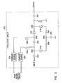
- FIG. 1 is a schematic diagram of an embodiment of a variable attenuator indicated generally at 100 and constructed according to the teachings of the present invention.
- Attenuator 100 includes attenuator circuit 102 and digital control circuit 104 .
- Digital control circuit 104 provides digital control signals to attenuator circuit 102 .
- the digital control signals set the current in a number of PIN diodes of attenuator circuit 102 . By setting the current in the PIN diodes, the attenuation level of attenuator circuit 102 is also established.
- variable attenuator 100 by incorporating digital control circuit 104 into variable attenuator 100 , the attenuation level provided to a signal path of an electronic system, e.g., network amplifier of a cable network, can be adjusted without the removal and replacement of an attenuation pad. Further, the attenuation level can be adjusted without the need to open the housing of the electronic system, e.g., network amplifier.
- an electronic system e.g., network amplifier of a cable network
- digital control circuit 104 uses values stored in a memory circuit to control the attenuation level of variable attenuator 100 .
- Digital control circuit 104 includes memory circuit 106 , processor 108 , and digital to analog converter (DAC) chip 110 .
- Memory circuit 106 , processor 108 , and DAC chip 110 are coupled to data bus 112 .
- DAC chip 110 includes first and second digital to analog converters (DACs) labeled DAC A and DAC B in FIG. 1 .
- DAC A and DAC B each provide a control signal to attenuator circuit 102 .
- memory circuit 106 is implemented as a non-volatile memory, such as an EEPROM, EPROM, Flash memory or other appropriate memory circuit.
- Memory circuit 106 stores a table of attenuation values and associated control signals for DAC A and DAC B that are used by attenuator circuit 102 to provide a selected attenuation level.
- the table may include control signals for attenuation levels from 0.25 dB to 10 dB in 0.25 dB steps. It is understood that control signals for other attenuation levels can be stored in memory circuit 106 as needed for a specific application.
- Processor 108 controls the flow of data from digital control circuit 104 to attenuator circuit 102 .
- Attenuator circuit 102 attenuates signals on a signal path using PIN diodes 116 , 118 , and 120 .
- PIN diodes 116 , 118 and 120 are coupled in a “T” configuration.
- PIN diodes are used in attenuator circuit 102 since, at radio frequencies (RF), a PIN diode acts as a variable resistor with a resistance value based on its bias current. It is noted that the PIN diodes can also be coupled in a “pi” configuration as shown in FIG. 2 .
- diodes 116 and 118 and capacitor 119 are coupled in series between INPUT and OUTPUT nodes of the signal path of attenuator circuit 102 .
- Diode 120 is coupled in series with capacitor 122 between node 121 and ground.
- Attenuator circuit 102 includes first and second current sources 124 and 126 to receive the control signals from digital control circuit 104 .
- Current source 126 is coupled through RF choke 128 to node 130 between capacitor 119 and PIN diode 116 .
- Current source 124 is coupled through RF choke 132 to node 134 between capacitor 122 and PIN diode 120 .
- Current sources 124 and 126 provide currents that are controlled by the voltage of the signals from DAC A and DAC B, respectively.
- digital control circuit 104 provides control signals to attenuator circuit 102 to establish a selected attenuation level for variable attenuator 100 .
- processor 108 looks in the look up table stored in memory circuit 106 to find the digital control signals associated with the desired attenuation level.
- Memory 106 places these values on data bus 112 .
- DAC A and DAC B receive these values from data bus 112 and convert the digital signals to analog control signals with specified voltage levels.
- Attenuator circuit 102 receives these analog control signals at current sources 124 and 126 .
- Current source 124 converts its control signal to establish a bias current for PIN diode 120 .
- Current source 126 converts its control signal to establish a bias current for PIN diodes 116 and 118 .
- the bias currents establish the resistance of PIN diodes 116 , 118 , and 120 and thus establish the attenuation level of variable attenuator 100 .
- the attenuation level can be changed at anytime by reading different digital control signals from memory 106 and applying the control signals to attenuator circuit 102 through DAC chip 110 .
- processor 108 uses interpolation to generate digital control signals for DAC chip 110 .
- processor 108 retrieves the digital control signals associated with the two closest attenuation values stored in memory 106 and performs a linear interpolation to establish control signals provided to DAC chip 110 .
- FIG. 2 is a schematic diagram of an alternative embodiment of an attenuator circuit, indicated generally at 202 , constructed according to the teachings of the present invention. As described above, attenuator circuit 202 is based on PIN diodes 216 , 218 , and 220 that are coupled in a “pi” configuration.
- diode 220 and capacitors 250 , 252 , and 254 are coupled in series between INPUT and OUTPUT nodes of the signal path of attenuator circuit 202 .
- Diodes 216 and 218 are coupled in series with resistors 256 and 258 between nodes 264 and 268 .
- Capacitor 260 is coupled between node 266 and ground.
- Attenuator circuit 202 includes current sources 224 and 236 .
- Current sources 224 and 236 are coupled to a digital control circuit such as, for example, digital control circuit 104 of FIG. 1 . It is understood that the digital control circuit can take on other configurations so long as the digital control circuit provides signals to attenuator circuit 202 that establish bias currents in PIN diodes 216 , 218 , and 220 to set a selected attenuation level.
- Current source 236 is coupled through RF choke 228 to node 262 .
- Current source 224 is coupled through RF choke 232 to node 264 .
- FIG. 3 is a schematic diagram of another embodiment of a variable attenuator, indicated generally at 300 , constructed according to the teachings of the present invention.
- Attenuator 300 includes digital control circuit 304 , adjustable attenuator stage 302 and fixed attenuator stage 303 .
- Digital control circuit 304 provides digital control signals to adjustable attenuator stage 302 .
- the digital control signals set the current in a number of PIN diodes of adjustable attenuator stage 302 . By setting the current in the PIN diodes, the attenuation level of adjustable attenuator stage 302 is also established.
- Fixed attenuator stage 303 is also provided on the signal path between INPUT and OUTPUT nodes.
- Fixed attenuator stage 303 is selectively switched into or out of the signal path. When fixed attenuator stage 303 is switched into the signal path, its fixed attenuation level is added to the attenuation level provided by adjustable attenuator stage 302 . Thereby, fixed attenuator stage 303 can be used to increase the range of attenuation levels provided by variable attenuator 300 .
- variable attenuator 300 by incorporating digital control circuit 304 into variable attenuator 300 , the attenuation level provided to a signal path of an electronic system, e.g., network amplifier of a cable network, can be adjusted without the removal and replacement of an attenuation pad. Further, the attenuation level can be adjusted without the need to open the housing of the electronic system, e.g., network amplifier.
- the range of variable attenuator 300 is double the range of adjustable attenuator stage 302 by including fixed attenuator stage 303 .
- variable attenuator 300 can provide an attenuation level between 0.25 and 16 dB in 0.25 dB steps.
- digital control circuit 304 uses values stored in a memory circuit to control the attenuation level of variable attenuator 300 .
- Digital control circuit 304 includes memory circuit 306 , processor 308 , and digital to analog converter (DAC) chip 310 .
- Memory circuit 306 , processor 308 , and DAC chip 310 are coupled to data bus 312 .
- DAC chip 310 includes first and second digital to analog converters with outputs labeled DAC A and DAC B in FIG. 3 .
- DAC A and DAC B each provide a control signal to adjustable attenuator stage 302 .
- DAC chip 310 also includes digital to analog converters with outputs labeled DAC C and DAC D that are used to control the switching in of fixed attenuator stage 303 .
- memory circuit 306 is implemented as a non-volatile memory, such as an EEPROM, EPROM, Flash memory or other appropriate memory circuit.
- Memory circuit 306 stores a table of attenuation values and associated control signals for DACs A, B, C, and D.
- the values provided to DACs A and B are used by adjustable attenuator stage 302 to provide a selected attenuation level.
- the table may include control signals for attenuation levels from 0.25 dB to 8 dB in 0.25 dB steps. It is understood that control signals for other attenuation levels can be stored in memory circuit 306 as needed for a specific application. This table can be generated using the technique described above with respect to FIG. 4 .
- the values provided to DACs C and D are used by fixed attenuator stage 303 to determine whether the fixed attenuator stage is to be switched into the signal path.
- Processor 308 controls the flow of data from digital control circuit 304 to adjustable attenuator stage 302 .
- Adjustable attenuator stage 302 attenuates signals on a signal path using PIN diodes 316 , 318 , and 320 .
- PIN diodes 316 , 318 and 320 are coupled in a “T” configuration.
- PIN diodes are used in adjustable attenuator stage 302 since, at radio frequencies (RF), a PIN diode acts as a variable resistor with a resistance value based on its bias current. It is noted that the PIN diodes can also be coupled in a “pi” configuration as shown and described with respect to FIG. 2 above.
- diodes 316 and 318 and capacitor 319 are coupled in series between INPUT node and node 340 of the signal path of adjustable attenuator stage 302 .
- Diode 320 is coupled in series with capacitor 322 between node 321 and ground.
- Adjustable attenuator stage 302 includes first and second current sources 324 and 326 that receive the control signals from digital control circuit 304 .
- Current source 326 is coupled through RF choke 328 to node 330 between capacitor 319 and PIN diode 316 .
- Current source 324 is coupled through RF choke 332 to node 334 between capacitor 322 and PIN diode 320 .
- Current sources 324 and 326 provide currents that are controlled by the voltage of the signals from DAC A and DAC B, respectively.
- Fixed attenuator stage 303 is provided to increase the range of variable attenuator 300 .
- Fixed attenuator stage 303 includes resistors 370 , 372 and 374 coupled in a “T” configuration to provide a fixed attenuation to be added to the attenuation level of adjustable attenuator stage 302 in the signal path between INPUT and OUTPUT nodes of variable attenuator 300 .
- Fixed attenuator stage 303 includes switches 378 and 382 that are coupled to receive control signals from digital control circuit 304 . These control signals, labeled DAC C and DAC D, respectively, control switches 378 and 382 to selectively bypass resistors 370 , 372 and 374 . When bypassed, fixed attenuator stage 303 provides no attenuation on signals passing between the INPUT and OUTPUT nodes of variable attenuator 300 . When not bypassed, fixed attenuator stage 303 adds a fixed attenuation level set by resistors 370 , 372 , and 374 .
- Fixed attenuator stage 303 provides, in one embodiment, a fixed attenuation level that is equal to the maximum attenuation level of adjustable attenuator stage 302 . This approximately doubles the range of the attenuation level for variable attenuator 300 .
- adjustable attenuator stage 302 can provide attenuation levels in the range from 0.25 dB to 8 dB in 0.25 dB steps
- the attenuation level of fixed attenuator stage 303 can be set at 8 dB.
- variable attenuator 300 can provide attenuation levels in the range from 0.25 dB to 16 dB with 0.25 dB steps.
- fixed attenuator stage 303 is bypassed for all attenuation levels below 8 dB.
- fixed attenuator stage 303 provides 8 dB of attenuation and adjustable attenuator stage 302 provides the remaining attenuation necessary to establish a selected attenuation level.
- the settings for adjustable attenuation stage 302 and fixed attenuation stage 303 are controlled by digital control circuit 304 based on digital control signals stored in memory 306 .
- digital control circuit 304 provides control signals to adjustable attenuator stage 302 and fixed attenuator stage 303 to establish a selected attenuation level for variable attenuator 300 .
- processor 308 looks in the look up table stored in memory circuit 306 to find the digital control signals associated with the desired attenuation level. Memory 306 places these values on data bus 312 .
- DACs 310 receive digital signals from data bus 312 and convert the digital signals to analog control signals with specified voltage levels to control the attenuation level of adjustable attenuation stage 302 via signals DAC A and DAC B.
- DACs 310 also receive digital signals from data bus 312 and convert the digital signals to analog control signals with specified voltage levels to selectively bypass fixed attenuation stage 302 via signals DAC C and DAC D.
- Adjustable attenuator stage 302 receives the DAC A and DAC B control signals at current sources 326 and 324 .
- Current source 324 converts its control signal to establish a bias current for PIN diode 320 .
- Current source 326 converts its control signal to establish a bias current for PIN diodes 316 and 318 .
- the bias currents establish the resistance of PIN diodes 316 , 318 , and 320 and thus establish the attenuation level of adjustable attenuator stage 302 .
- the attenuation level can be changed at anytime by reading different digital control signals from memory 306 and applying the control signals to adjustable attenuator stage 302 through DAC chip 310 .
- Fixed attenuator stage 303 receives control signals DAC C and DAC D at switches 378 and 382 , respectively. Based on these control signals, the effect of resistors 370 , 372 , and 374 on the signal path can be effectively bypassed. Alternatively, resistors 370 , 372 , and 374 can add to the attenuation level provided by adjustable attenuator stage 302 .
- interpolation can also be used with this embodiment to achieve attenuation levels not stored in memory 306 .
- the digital control circuit can take on other configurations that provide control signals to establish selected bias current levels in PIN diodes of an attenuator circuit.
- the memory circuit, DACs and processor described above can be replaced with other circuitry that stores and selectively delivers control signals to set the attenuation level of an attenuator circuit.
- the range of attenuation levels provided by the various stages and circuits can be adjusted as necessary for a particular application.
- the range of 0.25 dB to 8.0 dB with 0.25 dB steps is provided by way of example and not by way of limitation.
Abstract
Description
Claims (34)
Priority Applications (1)
| Application Number | Priority Date | Filing Date | Title |
|---|---|---|---|
| US09/609,076 US6339356B1 (en) | 1999-07-02 | 2000-06-30 | Variable attenuator |
Applications Claiming Priority (2)
| Application Number | Priority Date | Filing Date | Title |
|---|---|---|---|
| US14226799P | 1999-07-02 | 1999-07-02 | |
| US09/609,076 US6339356B1 (en) | 1999-07-02 | 2000-06-30 | Variable attenuator |
Publications (1)
| Publication Number | Publication Date |
|---|---|
| US6339356B1 true US6339356B1 (en) | 2002-01-15 |
Family
ID=26839922
Family Applications (1)
| Application Number | Title | Priority Date | Filing Date |
|---|---|---|---|
| US09/609,076 Expired - Lifetime US6339356B1 (en) | 1999-07-02 | 2000-06-30 | Variable attenuator |
Country Status (1)
| Country | Link |
|---|---|
| US (1) | US6339356B1 (en) |
Cited By (10)
| Publication number | Priority date | Publication date | Assignee | Title |
|---|---|---|---|---|
| US6836184B1 (en) | 1999-07-02 | 2004-12-28 | Adc Telecommunications, Inc. | Network amplifier with microprocessor control |
| US20060197577A1 (en) * | 2001-11-08 | 2006-09-07 | C-Cor Incorporated | Lossy linearizers for analog optical transmitters |
| US7430412B1 (en) | 2002-04-15 | 2008-09-30 | Steen Richard K | Digitally programmable continuously variable precision microwave attenuator |
| US20090213276A1 (en) * | 2005-01-31 | 2009-08-27 | Nxp B.V. | Receiver having a gain-controllable input stage |
| US20090264065A1 (en) * | 2008-04-18 | 2009-10-22 | Ec Telecom Co., Ltd. | Circuit for compensating passband flatness, apparatus and method for compensating passband flatness |
| US20120161843A1 (en) * | 2009-09-11 | 2012-06-28 | Mitsumi Electric Co., Ltd. | Attenuation control device, signal attenuation device, automatic gain control device, attenuation control method, and automatic gain control method |
| US20140034812A1 (en) * | 2011-04-21 | 2014-02-06 | Panasonic Corporation | Voltage generation circuit, analog-to-digital conversion circuit, solid-state imaging device, and imaging apparatus |
| US8744366B1 (en) | 2002-04-15 | 2014-06-03 | Richard K. Steen | Digitally programmable circuit for controlling an attenuator |
| US20160037188A1 (en) * | 2011-06-27 | 2016-02-04 | Trilithic, Inc. | Apparatus for detecting leakage in digitally modulated systems |
| US20220345916A1 (en) * | 2021-04-25 | 2022-10-27 | Fu Tai Hua Industry (Shenzhen) Co., Ltd. | Method, apparatus, and non-transitory computer readable medium for testing terminals |
Citations (5)
| Publication number | Priority date | Publication date | Assignee | Title |
|---|---|---|---|---|
| US5521560A (en) * | 1994-11-18 | 1996-05-28 | Hughes Aircraft Company | Minimum phase shift microwave attenuator |
| US5592470A (en) | 1994-12-21 | 1997-01-07 | At&T | Broadband wireless system and network architecture providing broadband/narrowband service with optimal static and dynamic bandwidth/channel allocation |
| US5656978A (en) * | 1995-12-11 | 1997-08-12 | Harmonic Lightwaves | Control circuit and method for direct current controlled attenuator |
| US5877653A (en) * | 1995-11-16 | 1999-03-02 | Samsung Electronics Co., Ltd. | Linear power amplifier and method for removing intermodulation distortion with predistortion system and feed forward system |
| US6133965A (en) * | 1998-02-12 | 2000-10-17 | Zenith Electronics Corporation | Digital AGC control for high definition television tuner |
-
2000
- 2000-06-30 US US09/609,076 patent/US6339356B1/en not_active Expired - Lifetime
Patent Citations (5)
| Publication number | Priority date | Publication date | Assignee | Title |
|---|---|---|---|---|
| US5521560A (en) * | 1994-11-18 | 1996-05-28 | Hughes Aircraft Company | Minimum phase shift microwave attenuator |
| US5592470A (en) | 1994-12-21 | 1997-01-07 | At&T | Broadband wireless system and network architecture providing broadband/narrowband service with optimal static and dynamic bandwidth/channel allocation |
| US5877653A (en) * | 1995-11-16 | 1999-03-02 | Samsung Electronics Co., Ltd. | Linear power amplifier and method for removing intermodulation distortion with predistortion system and feed forward system |
| US5656978A (en) * | 1995-12-11 | 1997-08-12 | Harmonic Lightwaves | Control circuit and method for direct current controlled attenuator |
| US6133965A (en) * | 1998-02-12 | 2000-10-17 | Zenith Electronics Corporation | Digital AGC control for high definition television tuner |
Non-Patent Citations (1)
| Title |
|---|
| "Siemans Application note on Silicon PIN Diodes", Jul., 1994. |
Cited By (15)
| Publication number | Priority date | Publication date | Assignee | Title |
|---|---|---|---|---|
| US6836184B1 (en) | 1999-07-02 | 2004-12-28 | Adc Telecommunications, Inc. | Network amplifier with microprocessor control |
| US20060197577A1 (en) * | 2001-11-08 | 2006-09-07 | C-Cor Incorporated | Lossy linearizers for analog optical transmitters |
| US7430412B1 (en) | 2002-04-15 | 2008-09-30 | Steen Richard K | Digitally programmable continuously variable precision microwave attenuator |
| US8744366B1 (en) | 2002-04-15 | 2014-06-03 | Richard K. Steen | Digitally programmable circuit for controlling an attenuator |
| US8331893B2 (en) * | 2005-01-31 | 2012-12-11 | Nxp B.V. | Receiver having a gain-controllable input stage |
| US20090213276A1 (en) * | 2005-01-31 | 2009-08-27 | Nxp B.V. | Receiver having a gain-controllable input stage |
| US20090264065A1 (en) * | 2008-04-18 | 2009-10-22 | Ec Telecom Co., Ltd. | Circuit for compensating passband flatness, apparatus and method for compensating passband flatness |
| US20120161843A1 (en) * | 2009-09-11 | 2012-06-28 | Mitsumi Electric Co., Ltd. | Attenuation control device, signal attenuation device, automatic gain control device, attenuation control method, and automatic gain control method |
| US20140034812A1 (en) * | 2011-04-21 | 2014-02-06 | Panasonic Corporation | Voltage generation circuit, analog-to-digital conversion circuit, solid-state imaging device, and imaging apparatus |
| US9232160B2 (en) * | 2011-04-21 | 2016-01-05 | Panasonic Intellectual Property Management Co., Ltd. | Voltage generation circuit, analog-to-digital conversion circuit, solid-state imaging device, and imaging apparatus, which are capable of reducing random noise |
| US20160037188A1 (en) * | 2011-06-27 | 2016-02-04 | Trilithic, Inc. | Apparatus for detecting leakage in digitally modulated systems |
| US9877050B2 (en) * | 2011-06-27 | 2018-01-23 | Trilithic, Inc. | Apparatus for detecting leakage in digitally modulated systems |
| US10334291B2 (en) | 2011-06-27 | 2019-06-25 | Viavi Solutions, Inc. | Apparatus for detecting leakage in digitally modulated systems |
| US20220345916A1 (en) * | 2021-04-25 | 2022-10-27 | Fu Tai Hua Industry (Shenzhen) Co., Ltd. | Method, apparatus, and non-transitory computer readable medium for testing terminals |
| US11696159B2 (en) * | 2021-04-25 | 2023-07-04 | Fu Tai Hua Industry (Shenzhen) Co., Ltd. | Method, apparatus, and non-transitory computer readable medium for testing terminals |
Similar Documents
| Publication | Publication Date | Title |
|---|---|---|
| KR100191101B1 (en) | Wide range variable output amplifier apparatus with high efficiency | |
| US6339356B1 (en) | Variable attenuator | |
| US6442281B2 (en) | Loudness volume control system | |
| EP1099303A1 (en) | Method and apparatus for controlling an audio signal level | |
| US6147558A (en) | Attenuating volume control | |
| US6919774B2 (en) | Broadband PIN diode attenuator bias network | |
| US5867063A (en) | Gain distribution circuit | |
| KR920000573B1 (en) | Video signal peaking control system with provision for automatic and manual control | |
| JP3600836B2 (en) | Network amplifier monitoring circuit | |
| AU7090098A (en) | Power amplifier and method therein | |
| US6018703A (en) | Software select and test | |
| US4439739A (en) | Circuit arrangement with electronically controllable transfer characteristic | |
| US6549087B1 (en) | Variable equalizer with independently controlled branches based on different frequency breakpoints | |
| US6836184B1 (en) | Network amplifier with microprocessor control | |
| WO2022173672A1 (en) | Adaptive cable equalizer | |
| EP0178821A2 (en) | Programmable automatic cable equalizer | |
| KR100623630B1 (en) | Apparatus and method for providing television receiver alignment functions | |
| US7795972B2 (en) | Automatic gain control apparatus and technique | |
| EP1327301B1 (en) | Amplification circuit with improved linearity | |
| JP5651266B1 (en) | Optical receiver AGC circuit and optical receiver with AGC circuit | |
| JPH0158886B2 (en) | ||
| US5150416A (en) | Electronic level control circuit for sound signals | |
| JP2944063B2 (en) | Filter device | |
| US4550265A (en) | Driver for voltage controlled attenuator | |
| JPH06216797A (en) | High frequency variable slope tilt circuit |
Legal Events
| Date | Code | Title | Description |
|---|---|---|---|
| AS | Assignment |
Owner name: ADC TELECOMMUNICATIONS, INC., MINNESOTA Free format text: ASSIGNMENT OF ASSIGNORS INTEREST;ASSIGNORS:DAUGHTRY, EARL A.;REESE, ROY CHARLES;REEL/FRAME:010939/0791;SIGNING DATES FROM 20000626 TO 20000628 |
|
| STCF | Information on status: patent grant |
Free format text: PATENTED CASE |
|
| AS | Assignment |
Owner name: ADC TELECOMMUNICATIONS, INC., MINNESOTA Free format text: CORRECTIV;ASSIGNORS:DAUGHTRY, EARL A.;REESE, ROY CHARLES;REEL/FRAME:012453/0415;SIGNING DATES FROM 20000626 TO 20000628 |
|
| FPAY | Fee payment |
Year of fee payment: 4 |
|
| FPAY | Fee payment |
Year of fee payment: 8 |
|
| FPAY | Fee payment |
Year of fee payment: 12 |
|
| AS | Assignment |
Owner name: TYCO ELECTRONICS SERVICES GMBH, SWITZERLAND Free format text: ASSIGNMENT OF ASSIGNORS INTEREST;ASSIGNOR:ADC TELECOMMUNICATIONS, INC.;REEL/FRAME:036060/0174 Effective date: 20110930 |
|
| AS | Assignment |
Owner name: COMMSCOPE EMEA LIMITED, IRELAND Free format text: ASSIGNMENT OF ASSIGNORS INTEREST;ASSIGNOR:TYCO ELECTRONICS SERVICES GMBH;REEL/FRAME:036956/0001 Effective date: 20150828 |
|
| AS | Assignment |
Owner name: COMMSCOPE TECHNOLOGIES LLC, NORTH CAROLINA Free format text: ASSIGNMENT OF ASSIGNORS INTEREST;ASSIGNOR:COMMSCOPE EMEA LIMITED;REEL/FRAME:037012/0001 Effective date: 20150828 |
|
| AS | Assignment |
Owner name: JPMORGAN CHASE BANK, N.A., AS COLLATERAL AGENT, ILLINOIS Free format text: PATENT SECURITY AGREEMENT (TERM);ASSIGNOR:COMMSCOPE TECHNOLOGIES LLC;REEL/FRAME:037513/0709 Effective date: 20151220 Owner name: JPMORGAN CHASE BANK, N.A., AS COLLATERAL AGENT, ILLINOIS Free format text: PATENT SECURITY AGREEMENT (ABL);ASSIGNOR:COMMSCOPE TECHNOLOGIES LLC;REEL/FRAME:037514/0196 Effective date: 20151220 Owner name: JPMORGAN CHASE BANK, N.A., AS COLLATERAL AGENT, IL Free format text: PATENT SECURITY AGREEMENT (ABL);ASSIGNOR:COMMSCOPE TECHNOLOGIES LLC;REEL/FRAME:037514/0196 Effective date: 20151220 Owner name: JPMORGAN CHASE BANK, N.A., AS COLLATERAL AGENT, IL Free format text: PATENT SECURITY AGREEMENT (TERM);ASSIGNOR:COMMSCOPE TECHNOLOGIES LLC;REEL/FRAME:037513/0709 Effective date: 20151220 |
|
| AS | Assignment |
Owner name: COMMSCOPE TECHNOLOGIES LLC, NORTH CAROLINA Free format text: RELEASE BY SECURED PARTY;ASSIGNOR:JPMORGAN CHASE BANK, N.A.;REEL/FRAME:048840/0001 Effective date: 20190404 Owner name: ANDREW LLC, NORTH CAROLINA Free format text: RELEASE BY SECURED PARTY;ASSIGNOR:JPMORGAN CHASE BANK, N.A.;REEL/FRAME:048840/0001 Effective date: 20190404 Owner name: REDWOOD SYSTEMS, INC., NORTH CAROLINA Free format text: RELEASE BY SECURED PARTY;ASSIGNOR:JPMORGAN CHASE BANK, N.A.;REEL/FRAME:048840/0001 Effective date: 20190404 Owner name: ALLEN TELECOM LLC, ILLINOIS Free format text: RELEASE BY SECURED PARTY;ASSIGNOR:JPMORGAN CHASE BANK, N.A.;REEL/FRAME:048840/0001 Effective date: 20190404 Owner name: COMMSCOPE, INC. OF NORTH CAROLINA, NORTH CAROLINA Free format text: RELEASE BY SECURED PARTY;ASSIGNOR:JPMORGAN CHASE BANK, N.A.;REEL/FRAME:048840/0001 Effective date: 20190404 Owner name: COMMSCOPE, INC. OF NORTH CAROLINA, NORTH CAROLINA Free format text: RELEASE BY SECURED PARTY;ASSIGNOR:JPMORGAN CHASE BANK, N.A.;REEL/FRAME:049260/0001 Effective date: 20190404 Owner name: COMMSCOPE TECHNOLOGIES LLC, NORTH CAROLINA Free format text: RELEASE BY SECURED PARTY;ASSIGNOR:JPMORGAN CHASE BANK, N.A.;REEL/FRAME:049260/0001 Effective date: 20190404 Owner name: ANDREW LLC, NORTH CAROLINA Free format text: RELEASE BY SECURED PARTY;ASSIGNOR:JPMORGAN CHASE BANK, N.A.;REEL/FRAME:049260/0001 Effective date: 20190404 Owner name: REDWOOD SYSTEMS, INC., NORTH CAROLINA Free format text: RELEASE BY SECURED PARTY;ASSIGNOR:JPMORGAN CHASE BANK, N.A.;REEL/FRAME:049260/0001 Effective date: 20190404 Owner name: ALLEN TELECOM LLC, ILLINOIS Free format text: RELEASE BY SECURED PARTY;ASSIGNOR:JPMORGAN CHASE BANK, N.A.;REEL/FRAME:049260/0001 Effective date: 20190404 |
|
| AS | Assignment |
Owner name: JPMORGAN CHASE BANK, N.A., NEW YORK Free format text: ABL SECURITY AGREEMENT;ASSIGNORS:COMMSCOPE, INC. OF NORTH CAROLINA;COMMSCOPE TECHNOLOGIES LLC;ARRIS ENTERPRISES LLC;AND OTHERS;REEL/FRAME:049892/0396 Effective date: 20190404 Owner name: JPMORGAN CHASE BANK, N.A., NEW YORK Free format text: TERM LOAN SECURITY AGREEMENT;ASSIGNORS:COMMSCOPE, INC. OF NORTH CAROLINA;COMMSCOPE TECHNOLOGIES LLC;ARRIS ENTERPRISES LLC;AND OTHERS;REEL/FRAME:049905/0504 Effective date: 20190404 Owner name: WILMINGTON TRUST, NATIONAL ASSOCIATION, AS COLLATE Free format text: PATENT SECURITY AGREEMENT;ASSIGNOR:COMMSCOPE TECHNOLOGIES LLC;REEL/FRAME:049892/0051 Effective date: 20190404 Owner name: WILMINGTON TRUST, NATIONAL ASSOCIATION, AS COLLATERAL AGENT, CONNECTICUT Free format text: PATENT SECURITY AGREEMENT;ASSIGNOR:COMMSCOPE TECHNOLOGIES LLC;REEL/FRAME:049892/0051 Effective date: 20190404 |