US6331783B1 - Circuit and method for improved test and calibration in automated test equipment - Google Patents
Circuit and method for improved test and calibration in automated test equipment Download PDFInfo
- Publication number
- US6331783B1 US6331783B1 US09/420,497 US42049799A US6331783B1 US 6331783 B1 US6331783 B1 US 6331783B1 US 42049799 A US42049799 A US 42049799A US 6331783 B1 US6331783 B1 US 6331783B1
- Authority
- US
- United States
- Prior art keywords
- circuit
- channel
- time varying
- solid state
- varying signal
- Prior art date
- Legal status (The legal status is an assumption and is not a legal conclusion. Google has not performed a legal analysis and makes no representation as to the accuracy of the status listed.)
- Expired - Lifetime
Links
Images


Classifications
-
- G—PHYSICS
- G01—MEASURING; TESTING
- G01R—MEASURING ELECTRIC VARIABLES; MEASURING MAGNETIC VARIABLES
- G01R31/00—Arrangements for testing electric properties; Arrangements for locating electric faults; Arrangements for electrical testing characterised by what is being tested not provided for elsewhere
- G01R31/28—Testing of electronic circuits, e.g. by signal tracer
- G01R31/317—Testing of digital circuits
- G01R31/3181—Functional testing
- G01R31/319—Tester hardware, i.e. output processing circuits
- G01R31/31903—Tester hardware, i.e. output processing circuits tester configuration
- G01R31/31908—Tester set-up, e.g. configuring the tester to the device under test [DUT], down loading test patterns
- G01R31/3191—Calibration
-
- G—PHYSICS
- G01—MEASURING; TESTING
- G01R—MEASURING ELECTRIC VARIABLES; MEASURING MAGNETIC VARIABLES
- G01R35/00—Testing or calibrating of apparatus covered by the other groups of this subclass
Definitions
- ATE Automatic test equipment or ATE is used to test semiconductor or other type devices at various stages of manufacture.
- An ATE tester generates signals, supplies the signals to a device under test or DUT, and monitors the responses to these signals to evaluate the fitness of the DUT.
- signals include DC signals, and time varying signals such as AC, pulsed, or other periodic signals.
- testers employ DC circuitry, and time varying signal circuitry sometimes referred to as pin electronics circuitry. Separate circuits are used because the circuits capable of providing and measuring precision DC signals are not capable of providing and measuring precision high frequency signals. Likewise, precision time varying signal circuits are not able to provide and measure precision DC signals. Thus, the tester must be capable of switching between these two circuits when testing a DUT.
- testers must be capable of performing self calibration.
- Self calibration includes signal level calibration as well as signal timing calibration. Thus, the tester also must provide this switching for calibration.
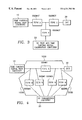
- FIG. 1 shows a “T” switching circuit commonly used in prior art ATE testers to perform such switching.
- Relays typically are employed to provide switching.
- Relay switches facilitate precision testing by providing low closed resistance and low open capacitance. This allows accurate transmission and measurement of signal timing and signal levels over a wide bandwidth and range of signal levels.
- the “T” switching circuit is able to provide low resistance and low capacitance transmission paths between the time varying signal circuitry 10 and the DUT 30 , between the DC test/time varying signal calibration circuitry 20 and the DUT 30 , as well as between the time varying signal circuitry 10 and the DC test/time varying signal calibration circuitry 20 .
- Relays have a significant drawback. Relays have a relatively low mean time before failure or MTBF as compared to other tester components.
- One cause of the low MTBF of relays is polymer build-up on the surface of the relay contacts. Contacts are susceptible to polymer build-up when switched dry rather than under an applied current or voltage. Such polymer build-up increases contact resistance. Moreover, the resistance caused by polymer build-up varies each time the contacts are closed. This is particularly true in relays designed for high bandwidth applications. In such applications, relays having small contacts to provide lower capacitance along the high frequency transmission line also have a reduced spring force, which facilitates resistance variations in polymerized contacts.
- relays In testers designed to test devices 125 Mhz-500 Mhz or greater, relays normally having only a fraction of an ohm resistance, can develop several ohms of resistance. This results in each closure of the relay leading to a different resistance value, which affects measurement precision and, consequently, the reliability of the tester. As such, relays contribute to tester down time, slowing production and reducing product margins. To compete in semiconductor and other electronic devices markets, manufacturers require more reliable test equipment.
- Solid state switches on the other hand, generally have orders of magnitude higher MTBF. Solid state switches, however, are not capable of providing the same low resistance and capacitance as relays.
- FIG. 2 illustrates a comparison of resistance verses capacitance characteristics of solid state switches and relays. Whereas the product of the closed resistance and open capacitance of a high frequency relay can be on the order of 0.07 pF-Ohms, the best commercially available solid state devices provide only about 15-40 pF-Ohms.
- a preferred embodiment of the present invention provides a switching circuit for testing and calibration in automated test equipment having a time varying signal channel, a DC test channel, and a time varying signal level calibration channel.
- the time varying signal channel has a series-connected solid state switch interposed between a time varying signal circuit end and a device under test end of the time varying signal channel.
- the DC test channel is connected to the time varying signal channel between the series-connected solid state switch and the device under test end.
- the DC test channel has at least one solid state switch interposed along the DC test channel so as to provide switchable coupling between a DC parametrics circuit side of the DC test channel and the time varying signal channel.
- the time varying signal level calibration channel is connected to the time varying signal channel between the series-connected solid state switch and the time varying signal circuit end.
- the signal level calibration channel has at least one solid state switch interposed along the signal level calibration channel so as to provide switchable coupling between a DC parametrics circuit side of the signal level calibration channel and the time varying signal channel.
- the DC test channel, the signal level calibration channel, or both may have a force branch and a sense branch each having a solid state switch.
- the time varying signal channel has a low resistance type solid state switch, while the DC test channel, the signal level calibration channel, or both, have low capacitance type solid state switches.
- FIG. 1 show a prior art test and calibration relay switching circuit.
- FIG. 2 illustrates a comparison of resistance and capacitance characteristics of a relay and solid state switches.
- FIG. 3 shows a possible implementation employing solid state switches.
- FIG. 4 shows a preferred embodiment of improved ATE test and calibration circuitry in accordance with the present invention.
- FIG. 5 shows a preferred embodiment of improved ATE test and calibration circuitry in accordance with the present invention.
- FIG. 3 shows a possible implementation to improve solid state switching.
- two types of solid state switches are used.
- a type A solid state switch having low resistance when closed and high capacitance when open and a TYPE B solid state switch having low capacitance when open and high resistance when closed.
- Type A switches, SSSW 1 T and SSSW 3 T couple the time varying signal circuitry 10 and the DUT 30 to form a time varying signal channel.
- a type B switch SSSW 2 T couples the DC test and time varying signal calibration circuitry to the time varying signal channel.
- the time varying signal channel transmission path resistance is provided through low resistance type A switches SSSW 1 and SSSW 3 , while the open type B switch SSSW 2 T, provides low capacitance along the time varying signal transmission path.
- DC signal testing of the DUT 30 is conducted via a high resistance type B switch SSSW 2 T. This reduces precision of DC signal testing of the DUT 30 . Further, this also occurs during calibration of the time varying signal circuitry 10 , as the time varying signal circuitry 10 is coupled to the calibration circuitry 20 via high resistance type SSSW 2 T.
- FIG. 4 shows a preferred embodiment of the present invention.
- a time varying signal channel 1030 connects the time varying signal circuitry 10 to the DUT 30 .
- the time varying signal channel 1030 has a series-connected solid state switch SSSW 1 capable of switchably coupling the time varying signal test circuitry 10 to the DUT 30 .
- a DC test channel 2530 is connected to the time varying signal channel 1030 so as to couple the DC parametric circuitry 25 to the DUT 30 .
- the DC test channel 2530 is connected to the time varying signal channel 1030 between the solid state switch SSSW 1 and a DUT end of the time varying signal channel 1030 .
- At least one solid state switch of SSSW 3 and SSSW 5 is interposed Ii; along the DC test channel 2530 so as to provide switchable coupling of the DC parametrics circuitry 25 to the DUT 30 .
- solid state switches SSSW 3 and SSSW 5 couple the DC parametric circuit 25 to the DUT 30 independent of, and not in series with, the series-connected switch SSSW 1 .
- a signal level calibration channel 1025 is connected to the time varying signal channel 1030 so as to couple the DC parametric circuitry 25 to the time varying signal circuitry 10 .
- At least one solid state switch of SSSW 2 and SSSW 4 is interposed along the signal level calibration channel 1025 so as to provide switchable coupling of the DC parametrics circuitry 25 to the time varying signal circuitry 10 .
- solid state switches SSSW 2 and SSSW 4 couple the DC parametric circuit 25 to the time varying signal circuit 10 independent of, and not in series with, the series-connected switch SSSW 1 .
- the configuration of FIG. 4 allows time varying and DC signal testing of the DUT 30 , self calibration of the time varying signal levels, as well as isolation of the time varying circuit 10 from the time varying signal channel 1030 for fault diagnosis.
- DUT testing using time varying signals is performed via the time varying signal channel 1030 , with SSSW 1 closed and SSSW 2 -SSSW 5 open.
- DC signal testing of the DUT 30 is performed via the DC test channel 2530 , with SSSW 3 and SSSW 5 closed and SSSW 1 , SSSW 2 , and SSSW 4 open.
- Calibration of time varyingsignal levels is performed via the signal level calibration channel 1025 , with SSSW 2 and SSSW 4 closed and SSSW 1 , SSSW 3 , and SSSW 5 open.
- this configuration it is possible to perform fault diagnosis of the time varying signal channel 1030 on its DUT side, between SSSW 1 and the DUT, by closing SSSW 1 .
- this isolation allows verification of the functionality of the terminals used to contact the time varying signal channel 1030 to the DUT 30 . Faults such as terminal shorting, for example, could be isolated with this embodiment.
- This capability is particularly desirable in ATE used for testing devices with high pin counts. For example, in ATE adapted to test 12,000 or more pins, isolation of the DUT side of the time varying signal channel 1030 is essential.
- low resistance type A and low capacitance type B solid state switches to provide improved channel characteristics when using solid state switches.
- a low closed resistance type A solid state switch is serially-connected in the time varying signal channel 1030 .
- Low open capacitance type B solid state switches are interposed along the DC test channel 2530 and the signal level calibration channel 1025 so as to provide switchable coupling between the DC parametrics circuit 25 and the time varying signal channel 1030 .
- the time varying signal passes through a low resistance switch SSSW 1 .
- switches SSSW 2 -SSSW 5 provide low capacitance when open during time varying signal testing.
- the embodiment of FIG. 4 provides a high bandwidth time varying signal channel 1030 , thus allowing high frequency signal transmission through the time varying signal channel 1030 .
- the solid state switch SSSW 1 proximate to the time varying signal circuitry 10 to facilitate signal transmission along the time varying signal channel 1030 .
- the sum of the output impedance of the time varying signal circuit 10 and the closed SSSW 1 appears the output impedance which is matched with the characteristic impedance of the DUT side of the time varying signal channel 1030 .
- an opto-coupled MOSFET or optically coupled metal oxide semiconductor field effect transistor switch having a closed resistance of about 2 to 3 Ohms is used.
- SSSW 1 is located about 1-2 cm from the time varying signal test circuitry 10 .
- DC signal testing of the DUT 30 and signal level calibration of the time varying signal is conducted via high resistance type B switches.
- DC testing and signal level calibration through high resistance type switches can unacceptably reduce measurement precision.
- SSSW 3 is provided in the force branch of the DC test channel 2530
- SSSW 5 is provided in the sense branch of DC test channel 2530 .
- the DC test channel 2530 sense branch provides feedback for controlling DC current or voltage at the sense branch connection to the time varying signal channel 1030 . Further, in the embodiment of FIG.
- SSSW 2 is provided in the force branch of the signal level calibration channel 1025
- SSSW 4 is provided in the sense branch of the signal level calibration channel 1025
- the signal level calibration channel 1025 sense branch provides feedback for controlling DC current or voltage at the sense branch connection to the time varying signal channel 1030 .
- the DC parametric circuitry 25 is capable of generating and evaluating signal levels using operation amplifiers 22 and 26 .
- a force voltage is applied to the non-inverting input of operational amplifier 22 .
- High resistance such as 10k Ohms, is provide in the feedback path.
- the operational amplifier 22 forces the voltage at point A′ to match the voltage at point A when testing the DUT, or forces the voltage at point A′′ to match the voltage at point A when performing signal level calibration of the time varying signal circuitry 10 .
- Another operational amplifier 24 detects current flow through resistor 27 and provides an output to an A/D converter for evaluation by a digital circuitry or computer (not shown).
- resistors 23 ′ and 23 ′′ are provided in the sense branches of the DC test and the signal level calibration channels 2530 and 1025 , respectively.
- the sense branches each include feedback resistance.
- precision DC voltage may be generated at point A′ for evaluation of DC performance of the DUT 30 , and at point A′′ for calibration of the voltage level of the time varying signal.
- SSSW 3 and SSSW 5 are located in the force and sense branches of the DC test channel 2530 , the high resistance of these switches does not affect the DC signal level at A′.
- the high resistance SSSW 2 and SSSW 4 located in the force and sense branches of the time varying signal level calibration channel 1025 , does not affect signal level at A′′.
- the voltage at A′ and A′′ is generated irrespective of switch resistance in the DC test and time varying signal level calibration channels 1030 and 1025 .
- the DC parametric circuitry 25 is utilized to calibrate the time varying signal level. It is preferred in this embodiment to provide separate timing calibration circuitry 40 for calibrating the timing characteristics of the time varying signal circuit 10 .
- the time calibration circuit may be coupled to the time varying signal channel 1030 via switch SW 6 , such as a relay or a solid state switch. Variations in signal level at the timing calibration circuitry 40 is not critical to timing calibration as is the case in signal level calibration. Thus, build-up on a relay contact is not critical because the time varying signal level is calibrated separately by the DC parametrics circuitry 25 via the signal level calibration channel 1025 .
- the timing calibration circuit 40 may include a time domain reflectometer or TDR for determining the path length of the time varying signal channel 1030 for use in timing calibration.
- the time varying signals are supplied by pattern and timing circuits 18 and 16 to an output buffer 12 for transmission along the time varying signal channel 1030 .
- the time varying signal may be A/C, pulsed, or the like.
- An input buffer 14 receives signals from the time varying signal channel 1030 and provides them to the timing and pattern circuits 16 and 18 for evaluation.
- any kind of solid state switch appropriate for the desired test signal frequency and levels may be utilized for SSSW 1 -SSSW 5 .
- the solid state switches all may be a single kind of switch, or different kinds may be utilized in different positions.
- all optically coupled metal oxide semiconductor field effect transistor switches, pin diode switches, or the like may be utilized.
- one kind of solid state switch fabricated as a low capacitance type switch may be used in the DC test and signal level calibration channels 2530 and 1025
- another kind of solid state switch fabricated as a low resistance type switch may be used in the time varying signal channel 1030 .
- optically coupled metal oxide semiconductor field effect transistor switches could be used for SSSW 2 -SSSW 5 while a pin diode could be used for SSSW 1 .
Landscapes
- Physics & Mathematics (AREA)
- General Physics & Mathematics (AREA)
- Engineering & Computer Science (AREA)
- General Engineering & Computer Science (AREA)
- Tests Of Electronic Circuits (AREA)
Abstract
Description
Claims (34)
Priority Applications (9)
| Application Number | Priority Date | Filing Date | Title |
|---|---|---|---|
| US09/420,497 US6331783B1 (en) | 1999-10-19 | 1999-10-19 | Circuit and method for improved test and calibration in automated test equipment |
| TW089121793A TW589463B (en) | 1999-10-19 | 2000-10-18 | Circuit and method for improved test and calibration in automated test equipment |
| JP2001532112A JP4689125B2 (en) | 1999-10-19 | 2000-10-18 | Improved test and calibration circuit and method in automatic test equipment |
| DE60025247T DE60025247T2 (en) | 1999-10-19 | 2000-10-18 | CIRCUIT AND METHOD FOR TESTING AND CALIBRATION |
| PCT/US2000/028915 WO2001029571A1 (en) | 1999-10-19 | 2000-10-18 | Circuit and method for improved test and calibration in automated test equipment |
| AT00972272T ATE314661T1 (en) | 1999-10-19 | 2000-10-18 | CIRCUIT AND METHOD FOR TESTING AND CALIBRATION |
| KR1020027005004A KR100731344B1 (en) | 1999-10-19 | 2000-10-18 | Circuit and method for improved test and calibration in automated test equipment |
| EP00972272A EP1224487B1 (en) | 1999-10-19 | 2000-10-18 | Circuit and method for improved test and calibration in automated test equipment |
| MYPI20004913A MY124977A (en) | 1999-10-19 | 2000-10-19 | Circuit and method for improved test and calibration in automated test equipment |
Applications Claiming Priority (1)
| Application Number | Priority Date | Filing Date | Title |
|---|---|---|---|
| US09/420,497 US6331783B1 (en) | 1999-10-19 | 1999-10-19 | Circuit and method for improved test and calibration in automated test equipment |
Publications (1)
| Publication Number | Publication Date |
|---|---|
| US6331783B1 true US6331783B1 (en) | 2001-12-18 |
Family
ID=23666728
Family Applications (1)
| Application Number | Title | Priority Date | Filing Date |
|---|---|---|---|
| US09/420,497 Expired - Lifetime US6331783B1 (en) | 1999-10-19 | 1999-10-19 | Circuit and method for improved test and calibration in automated test equipment |
Country Status (9)
| Country | Link |
|---|---|
| US (1) | US6331783B1 (en) |
| EP (1) | EP1224487B1 (en) |
| JP (1) | JP4689125B2 (en) |
| KR (1) | KR100731344B1 (en) |
| AT (1) | ATE314661T1 (en) |
| DE (1) | DE60025247T2 (en) |
| MY (1) | MY124977A (en) |
| TW (1) | TW589463B (en) |
| WO (1) | WO2001029571A1 (en) |
Cited By (18)
| Publication number | Priority date | Publication date | Assignee | Title |
|---|---|---|---|---|
| US6469514B2 (en) * | 2000-04-04 | 2002-10-22 | Advantest Corporation | Timing calibration apparatus and method in a semiconductor integrated circuit tester |
| US20030028343A1 (en) * | 2001-05-23 | 2003-02-06 | Micron Technology, Inc. | Intelligent measurement modular semiconductor parametric test system |
| US6563298B1 (en) | 2000-08-15 | 2003-05-13 | Ltx Corporation | Separating device response signals from composite signals |
| US20030110427A1 (en) * | 2000-04-12 | 2003-06-12 | Advantest Corporation | Semiconductor test system storing pin calibration data in non-volatile memory |
| US6586924B1 (en) * | 1999-08-16 | 2003-07-01 | Advantest Corporation | Method for correcting timing for IC tester and IC tester having correcting function using the correcting method |
| US20030212523A1 (en) * | 2002-04-25 | 2003-11-13 | Micron Technology, Inc. | Dynamically adaptable semiconductor parametric testing |
| US6661242B1 (en) * | 2001-12-20 | 2003-12-09 | Xilinx, Inc. | Using a DUT pin at known voltage to determine channel path resistance in automated test equipment test channels |
| US20040181731A1 (en) * | 2000-04-12 | 2004-09-16 | Advantest Corporation | Semiconductor test system storing pin calibration data, commands and other data in non-volatile memory |
| US20040189339A1 (en) * | 2003-03-31 | 2004-09-30 | Conner George W. | Hybrid AC/DC-coupled channel for automatic test equipment |
| US20040210413A1 (en) * | 2003-04-17 | 2004-10-21 | Micron Technology, Inc. | Dynamic creation and modification of wafer test maps during wafer testing |
| US20050088197A1 (en) * | 2002-12-18 | 2005-04-28 | Teradyne, Inc. | Pin driver for AC and DC semiconductor device testing |
| US20060279314A1 (en) * | 2005-06-08 | 2006-12-14 | Samsung Electronics Co., Ltd. | Test supporting device and method of testing using the same |
| US20060279310A1 (en) * | 2004-12-21 | 2006-12-14 | Teradyne, Inc. | Method and system for monitoring test signals for semiconductor devices |
| US20080174331A1 (en) * | 2007-01-19 | 2008-07-24 | King Yuan Electronics Co., Ltd. | Structure of test area for a semiconductor tester |
| US20080243740A1 (en) * | 2007-04-02 | 2008-10-02 | Hauptman Steven L | Calibrating A Tester Using ESD Protection Circuitry |
| CN102944858A (en) * | 2012-11-12 | 2013-02-27 | 无锡市计量测试中心 | Residual current device action characteristic detector calibration instrument separating switch |
| WO2013068040A1 (en) * | 2011-11-09 | 2013-05-16 | Advantest (Singapore) Pte. Ltd. | Concept for extracting a signal being exchanged between a device under test and an automatic test equipment |
| TWI490512B (en) * | 2013-11-28 | 2015-07-01 | 英業達股份有限公司 | Signal circuit board and test circuit board disposing system and method thereof |
Families Citing this family (4)
| Publication number | Priority date | Publication date | Assignee | Title |
|---|---|---|---|---|
| US6570397B2 (en) | 2001-08-07 | 2003-05-27 | Agilent Technologies, Inc. | Timing calibration and timing calibration verification of electronic circuit testers |
| DE10335164B4 (en) | 2003-07-30 | 2007-03-22 | Infineon Technologies Ag | Apparatus and method for parallel testing of multiple integrated circuits |
| KR101279737B1 (en) * | 2012-03-29 | 2013-06-27 | 주식회사 에프티랩 | The inspection apparatus for the capacitive touch screen panel using switching device and the inspection method using the same |
| CN104656003B (en) * | 2013-11-22 | 2017-07-07 | 英业达科技有限公司 | Signal circuit board configures system and method with test circuit plate |
Citations (12)
| Publication number | Priority date | Publication date | Assignee | Title |
|---|---|---|---|---|
| US4354268A (en) * | 1980-04-03 | 1982-10-12 | Santek, Inc. | Intelligent test head for automatic test system |
| US4799008A (en) | 1986-04-14 | 1989-01-17 | Advantest Corporation | AC level calibration apparatus |
| US4806852A (en) * | 1984-09-07 | 1989-02-21 | Megatest Corporation | Automatic test system with enhanced performance of timing generators |
| US5101153A (en) | 1991-01-09 | 1992-03-31 | National Semiconductor Corporation | Pin electronics test circuit for IC device testing |
| US5389990A (en) | 1989-10-21 | 1995-02-14 | Kabushiki Kaisha Toshiba | Method for measuring DC current/voltage characteristic of semiconductor device |
| US5402079A (en) | 1992-12-18 | 1995-03-28 | Vlsi Technology, Inc. | Integrated circuit relay control system |
| US5621329A (en) | 1995-04-13 | 1997-04-15 | Industrial Technology Research Institute | Automatic self-calibration system for digital teraohmmeter |
| JPH09281188A (en) | 1996-04-15 | 1997-10-31 | Advantest Corp | Ic-testing apparatus |
| US5812424A (en) | 1995-10-31 | 1998-09-22 | Ando Electric Co., Ltd. | Relay control circuit |
| US5821529A (en) | 1996-04-10 | 1998-10-13 | Advantest Corporation | Measuring board having an optically driven switch and I/O terminal testing system using the same |
| US5917331A (en) | 1995-10-23 | 1999-06-29 | Megatest Corporation | Integrated circuit test method and structure |
| US6133725A (en) * | 1998-03-26 | 2000-10-17 | Teradyne, Inc. | Compensating for the effects of round-trip delay in automatic test equipment |
Family Cites Families (5)
| Publication number | Priority date | Publication date | Assignee | Title |
|---|---|---|---|---|
| JP2515914Y2 (en) * | 1988-06-15 | 1996-11-06 | 株式会社アドバンテスト | IC tester timing calibration device |
| JPH0712940Y2 (en) * | 1989-11-06 | 1995-03-29 | 株式会社アドバンテスト | IC test equipment |
| US5200696A (en) * | 1990-09-10 | 1993-04-06 | Ltx Corporation | Test system apparatus with Schottky diodes with programmable voltages |
| JP3075135B2 (en) * | 1995-04-14 | 2000-08-07 | 横河電機株式会社 | LSI tester |
| JPH1082837A (en) * | 1996-09-06 | 1998-03-31 | Advantest Corp | Lsi test device |
-
1999
- 1999-10-19 US US09/420,497 patent/US6331783B1/en not_active Expired - Lifetime
-
2000
- 2000-10-18 EP EP00972272A patent/EP1224487B1/en not_active Expired - Lifetime
- 2000-10-18 KR KR1020027005004A patent/KR100731344B1/en active IP Right Grant
- 2000-10-18 DE DE60025247T patent/DE60025247T2/en not_active Expired - Fee Related
- 2000-10-18 TW TW089121793A patent/TW589463B/en not_active IP Right Cessation
- 2000-10-18 AT AT00972272T patent/ATE314661T1/en not_active IP Right Cessation
- 2000-10-18 JP JP2001532112A patent/JP4689125B2/en not_active Expired - Lifetime
- 2000-10-18 WO PCT/US2000/028915 patent/WO2001029571A1/en active IP Right Grant
- 2000-10-19 MY MYPI20004913A patent/MY124977A/en unknown
Patent Citations (12)
| Publication number | Priority date | Publication date | Assignee | Title |
|---|---|---|---|---|
| US4354268A (en) * | 1980-04-03 | 1982-10-12 | Santek, Inc. | Intelligent test head for automatic test system |
| US4806852A (en) * | 1984-09-07 | 1989-02-21 | Megatest Corporation | Automatic test system with enhanced performance of timing generators |
| US4799008A (en) | 1986-04-14 | 1989-01-17 | Advantest Corporation | AC level calibration apparatus |
| US5389990A (en) | 1989-10-21 | 1995-02-14 | Kabushiki Kaisha Toshiba | Method for measuring DC current/voltage characteristic of semiconductor device |
| US5101153A (en) | 1991-01-09 | 1992-03-31 | National Semiconductor Corporation | Pin electronics test circuit for IC device testing |
| US5402079A (en) | 1992-12-18 | 1995-03-28 | Vlsi Technology, Inc. | Integrated circuit relay control system |
| US5621329A (en) | 1995-04-13 | 1997-04-15 | Industrial Technology Research Institute | Automatic self-calibration system for digital teraohmmeter |
| US5917331A (en) | 1995-10-23 | 1999-06-29 | Megatest Corporation | Integrated circuit test method and structure |
| US5812424A (en) | 1995-10-31 | 1998-09-22 | Ando Electric Co., Ltd. | Relay control circuit |
| US5821529A (en) | 1996-04-10 | 1998-10-13 | Advantest Corporation | Measuring board having an optically driven switch and I/O terminal testing system using the same |
| JPH09281188A (en) | 1996-04-15 | 1997-10-31 | Advantest Corp | Ic-testing apparatus |
| US6133725A (en) * | 1998-03-26 | 2000-10-17 | Teradyne, Inc. | Compensating for the effects of round-trip delay in automatic test equipment |
Non-Patent Citations (2)
| Title |
|---|
| Aromat Corporation, "Photo MOS Relay is being used to replace reed relay", view slide fax, Jun. 20, 1997 (best available copy). |
| Patents Abstracts of Japan, vol. 1998, No. 02, Jan. 30, 1998 & JP 09281188A (Advantest Corp.), Oct. 31, 1997 abstract. |
Cited By (40)
| Publication number | Priority date | Publication date | Assignee | Title |
|---|---|---|---|---|
| US6586924B1 (en) * | 1999-08-16 | 2003-07-01 | Advantest Corporation | Method for correcting timing for IC tester and IC tester having correcting function using the correcting method |
| US6469514B2 (en) * | 2000-04-04 | 2002-10-22 | Advantest Corporation | Timing calibration apparatus and method in a semiconductor integrated circuit tester |
| US20030110427A1 (en) * | 2000-04-12 | 2003-06-12 | Advantest Corporation | Semiconductor test system storing pin calibration data in non-volatile memory |
| US20040181731A1 (en) * | 2000-04-12 | 2004-09-16 | Advantest Corporation | Semiconductor test system storing pin calibration data, commands and other data in non-volatile memory |
| US6563298B1 (en) | 2000-08-15 | 2003-05-13 | Ltx Corporation | Separating device response signals from composite signals |
| US6703825B1 (en) | 2000-08-15 | 2004-03-09 | Ltx Corporation | Separating device response signals from composite signals |
| US20030028343A1 (en) * | 2001-05-23 | 2003-02-06 | Micron Technology, Inc. | Intelligent measurement modular semiconductor parametric test system |
| US7337088B2 (en) | 2001-05-23 | 2008-02-26 | Micron Technology, Inc. | Intelligent measurement modular semiconductor parametric test system |
| US6661242B1 (en) * | 2001-12-20 | 2003-12-09 | Xilinx, Inc. | Using a DUT pin at known voltage to determine channel path resistance in automated test equipment test channels |
| US20030212523A1 (en) * | 2002-04-25 | 2003-11-13 | Micron Technology, Inc. | Dynamically adaptable semiconductor parametric testing |
| US20060125509A1 (en) * | 2002-04-25 | 2006-06-15 | Micron Technology, Inc. | Dynamically adaptable semiconductor parametric testing |
| US20050021273A1 (en) * | 2002-04-25 | 2005-01-27 | Micron Technology, Inc. | Dynamically adaptable semiconductor parametric testing |
| US7165004B2 (en) | 2002-04-25 | 2007-01-16 | Micron Technology, Inc. | Dynamically adaptable semiconductor parametric testing |
| US7139672B2 (en) | 2002-04-25 | 2006-11-21 | Micron Technology, Inc. | Dynamically adaptable semiconductor parametric testing |
| US20060122803A1 (en) * | 2002-04-25 | 2006-06-08 | Micron Technology, Inc. | Dynamically adaptable semiconductor parametric testing |
| US7383147B2 (en) | 2002-04-25 | 2008-06-03 | Micron Technology, Inc. | Dynamically adaptable semiconductor parametric testing |
| US7162386B2 (en) | 2002-04-25 | 2007-01-09 | Micron Technology, Inc. | Dynamically adaptable semiconductor parametric testing |
| US7019547B2 (en) * | 2002-12-18 | 2006-03-28 | Teradyne, Inc. | Pin driver for AC and DC semiconductor device testing |
| US20050088197A1 (en) * | 2002-12-18 | 2005-04-28 | Teradyne, Inc. | Pin driver for AC and DC semiconductor device testing |
| US20050140388A1 (en) * | 2003-03-31 | 2005-06-30 | Conner George W. | Hybrid AC/DC-coupled channel for testing |
| US20040189339A1 (en) * | 2003-03-31 | 2004-09-30 | Conner George W. | Hybrid AC/DC-coupled channel for automatic test equipment |
| US7208937B2 (en) | 2003-03-31 | 2007-04-24 | Teradyne, Inc. | Hybrid AC/DC-coupled channel for testing |
| US6879175B2 (en) * | 2003-03-31 | 2005-04-12 | Teradyne, Inc. | Hybrid AC/DC-coupled channel for automatic test equipment |
| US20040210413A1 (en) * | 2003-04-17 | 2004-10-21 | Micron Technology, Inc. | Dynamic creation and modification of wafer test maps during wafer testing |
| US20060064268A1 (en) * | 2003-04-17 | 2006-03-23 | Micron Technology, Inc. | Dynamic creation and modification of wafer test maps during wafer testing |
| US7010451B2 (en) | 2003-04-17 | 2006-03-07 | Micron Technology, Inc. | Dynamic creation and modification of wafer test maps during wafer testing |
| US7508228B2 (en) * | 2004-12-21 | 2009-03-24 | Teradyne, Inc. | Method and system for monitoring test signals for semiconductor devices |
| US20060279310A1 (en) * | 2004-12-21 | 2006-12-14 | Teradyne, Inc. | Method and system for monitoring test signals for semiconductor devices |
| US20060279314A1 (en) * | 2005-06-08 | 2006-12-14 | Samsung Electronics Co., Ltd. | Test supporting device and method of testing using the same |
| US20080174331A1 (en) * | 2007-01-19 | 2008-07-24 | King Yuan Electronics Co., Ltd. | Structure of test area for a semiconductor tester |
| US7489125B2 (en) * | 2007-04-02 | 2009-02-10 | Teradyne, Inc. | Calibrating a tester using ESD protection circuitry |
| US20080243740A1 (en) * | 2007-04-02 | 2008-10-02 | Hauptman Steven L | Calibrating A Tester Using ESD Protection Circuitry |
| TWI416138B (en) * | 2007-04-02 | 2013-11-21 | Teradyne Inc | Calibrating a tester using esd protection circuitry |
| CN103917880B (en) * | 2011-11-09 | 2016-06-08 | 爱德万测试公司 | For being extracted in the concept of the signal swapped between measured device and ATE |
| WO2013068040A1 (en) * | 2011-11-09 | 2013-05-16 | Advantest (Singapore) Pte. Ltd. | Concept for extracting a signal being exchanged between a device under test and an automatic test equipment |
| CN103917880A (en) * | 2011-11-09 | 2014-07-09 | 爱德万测试(新加坡)私人有限公司 | Concept for extracting a signal being exchanged between a device under test and an automatic test equipment |
| US9568498B2 (en) | 2011-11-09 | 2017-02-14 | Advantest Corporation | Concept for extracting a signal being exchanged between a device under test and an automatic test equipment |
| CN102944858A (en) * | 2012-11-12 | 2013-02-27 | 无锡市计量测试中心 | Residual current device action characteristic detector calibration instrument separating switch |
| CN102944858B (en) * | 2012-11-12 | 2014-12-03 | 无锡市计量测试中心 | Residual current device action characteristic detector calibration instrument separating switch |
| TWI490512B (en) * | 2013-11-28 | 2015-07-01 | 英業達股份有限公司 | Signal circuit board and test circuit board disposing system and method thereof |
Also Published As
| Publication number | Publication date |
|---|---|
| KR100731344B1 (en) | 2007-06-21 |
| DE60025247D1 (en) | 2006-02-02 |
| WO2001029571A1 (en) | 2001-04-26 |
| EP1224487A1 (en) | 2002-07-24 |
| KR20020062630A (en) | 2002-07-26 |
| TW589463B (en) | 2004-06-01 |
| JP4689125B2 (en) | 2011-05-25 |
| MY124977A (en) | 2006-07-31 |
| DE60025247T2 (en) | 2006-08-31 |
| EP1224487B1 (en) | 2005-12-28 |
| JP2003512630A (en) | 2003-04-02 |
| ATE314661T1 (en) | 2006-01-15 |
Similar Documents
| Publication | Publication Date | Title |
|---|---|---|
| US6331783B1 (en) | Circuit and method for improved test and calibration in automated test equipment | |
| US6051979A (en) | System and method for detecting shorts, opens and connected pins on a printed circuit board using automatic test equipment | |
| US7068061B2 (en) | Semiconductor device characteristics measurement apparatus and connection apparatus | |
| JP3966562B2 (en) | RF signal automatic test equipment architecture | |
| US7880486B2 (en) | Method and apparatus for increasing operating frequency of a system for testing electronic devices | |
| KR101207090B1 (en) | Method and apparatus for remotely buffering test channels | |
| US6417682B1 (en) | Semiconductor device testing apparatus and its calibration method | |
| KR101257246B1 (en) | Pin electronics driver | |
| EP2562932A1 (en) | Integrated circuit | |
| US20110156730A1 (en) | Chip-based prober for high frequency measurements and methods of measuring | |
| JPH01250077A (en) | Method and apparatus for checking connectability between circuit board and test jig | |
| JP2011196813A (en) | Method and system of testing semiconductor integrated circuit | |
| US6833722B2 (en) | Electronic circuit device with a short circuit switch using transistors and method of testing such a device | |
| US7679390B2 (en) | Test apparatus and pin electronics card | |
| CN111208410A (en) | Voltage and current source test circuit and test method | |
| CN211741497U (en) | Voltage current source test circuit | |
| US7615990B1 (en) | Loadboard enhancements for automated test equipment | |
| JPH10293153A (en) | Impedance matching circuit |
Legal Events
| Date | Code | Title | Description |
|---|---|---|---|
| AS | Assignment |
Owner name: TERADYNE, INC., MASSACHUSETTS Free format text: ASSIGNMENT OF ASSIGNORS INTEREST;ASSIGNOR:HAUPTMAN, STEVEN;REEL/FRAME:010369/0718 Effective date: 19991026 |
|
| STCF | Information on status: patent grant |
Free format text: PATENTED CASE |
|
| FEPP | Fee payment procedure |
Free format text: PAYOR NUMBER ASSIGNED (ORIGINAL EVENT CODE: ASPN); ENTITY STATUS OF PATENT OWNER: LARGE ENTITY |
|
| FPAY | Fee payment |
Year of fee payment: 4 |
|
| AS | Assignment |
Owner name: BANK OF AMERICA, N.A., AS ADMINISTRATIVE AGENT, TE Free format text: NOTICE OF GRANT OF SECURITY INTEREST IN PATENTS;ASSIGNOR:TERADYNE, INC.;REEL/FRAME:021912/0762 Effective date: 20081114 Owner name: BANK OF AMERICA, N.A., AS ADMINISTRATIVE AGENT,TEX Free format text: NOTICE OF GRANT OF SECURITY INTEREST IN PATENTS;ASSIGNOR:TERADYNE, INC.;REEL/FRAME:021912/0762 Effective date: 20081114 |
|
| AS | Assignment |
Owner name: TERADYNE, INC, MASSACHUSETTS Free format text: RELEASE BY SECURED PARTY;ASSIGNOR:BANK OF AMERICA, N.A.;REEL/FRAME:022668/0750 Effective date: 20090427 Owner name: TERADYNE, INC,MASSACHUSETTS Free format text: RELEASE BY SECURED PARTY;ASSIGNOR:BANK OF AMERICA, N.A.;REEL/FRAME:022668/0750 Effective date: 20090427 |
|
| FPAY | Fee payment |
Year of fee payment: 8 |
|
| FPAY | Fee payment |
Year of fee payment: 12 |
|
| AS | Assignment |
Owner name: BARCLAYS BANK PLC, NEW YORK Free format text: PATENT SECURITY AGREEMENT;ASSIGNORS:TERADYNE, INC.;LITEPOINT CORPORATION;REEL/FRAME:035507/0116 Effective date: 20150427 |
|
| AS | Assignment |
Owner name: LITEPOINT CORPORATION, CALIFORNIA Free format text: RELEASE OF SECURITY INTEREST IN INTELLECTUAL PROPERTY;ASSIGNOR:BARCLAYS BANK PLC, AS COLLATERAL AGENT;REEL/FRAME:049632/0940 Effective date: 20190627 Owner name: GENRAD, LLC, MASSACHUSETTS Free format text: RELEASE OF SECURITY INTEREST IN INTELLECTUAL PROPERTY;ASSIGNOR:BARCLAYS BANK PLC, AS COLLATERAL AGENT;REEL/FRAME:049632/0940 Effective date: 20190627 Owner name: NEXTEST SYSTEMS CORPORATION, CALIFORNIA Free format text: RELEASE OF SECURITY INTEREST IN INTELLECTUAL PROPERTY;ASSIGNOR:BARCLAYS BANK PLC, AS COLLATERAL AGENT;REEL/FRAME:049632/0940 Effective date: 20190627 Owner name: TERADYNE, INC., MASSACHUSETTS Free format text: RELEASE OF SECURITY INTEREST IN INTELLECTUAL PROPERTY;ASSIGNOR:BARCLAYS BANK PLC, AS COLLATERAL AGENT;REEL/FRAME:049632/0940 Effective date: 20190627 Owner name: ENERGID TECHNOLOGIES CORPORATION, MASSACHUSETTS Free format text: RELEASE OF SECURITY INTEREST IN INTELLECTUAL PROPERTY;ASSIGNOR:BARCLAYS BANK PLC, AS COLLATERAL AGENT;REEL/FRAME:049632/0940 Effective date: 20190627 Owner name: EAGLE TEST SYSTEMS, INC., ILLINOIS Free format text: RELEASE OF SECURITY INTEREST IN INTELLECTUAL PROPERTY;ASSIGNOR:BARCLAYS BANK PLC, AS COLLATERAL AGENT;REEL/FRAME:049632/0940 Effective date: 20190627 |
|
| AS | Assignment |
Owner name: TRUIST BANK, GEORGIA Free format text: SECURITY INTEREST;ASSIGNOR:TERADYNE, INC.;REEL/FRAME:052595/0632 Effective date: 20200501 |