US6304958B1 - Microcomputer having data execution units mounted thereon - Google Patents
Microcomputer having data execution units mounted thereon Download PDFInfo
- Publication number
- US6304958B1 US6304958B1 US09/210,886 US21088698A US6304958B1 US 6304958 B1 US6304958 B1 US 6304958B1 US 21088698 A US21088698 A US 21088698A US 6304958 B1 US6304958 B1 US 6304958B1
- Authority
- US
- United States
- Prior art keywords
- data
- memory
- execution unit
- unit
- address
- Prior art date
- Legal status (The legal status is an assumption and is not a legal conclusion. Google has not performed a legal analysis and makes no representation as to the accuracy of the status listed.)
- Expired - Lifetime
Links
- 230000015654 memory Effects 0.000 claims abstract description 863
- 238000012545 processing Methods 0.000 claims abstract description 100
- 239000004065 semiconductor Substances 0.000 claims abstract description 5
- 239000000758 substrate Substances 0.000 claims abstract description 5
- 230000005540 biological transmission Effects 0.000 claims 6
- ORPUAOXOPLNKNG-GEUQSOIWSA-N mycinamicin VI Chemical compound O([C@@H]1[C@@H](C)/C=C/C(=O)O[C@@H]([C@H](/C=C/C=C/C(=O)[C@H](C)C[C@@H]1C)CO[C@H]1[C@@H]([C@H](O)[C@H](O)[C@@H](C)O1)O)CC)[C@@H]1O[C@H](C)C[C@H](N(C)C)[C@H]1O ORPUAOXOPLNKNG-GEUQSOIWSA-N 0.000 description 729
- 101100286247 Mus musculus Id1 gene Proteins 0.000 description 209
- 101100286255 Mus musculus Id2 gene Proteins 0.000 description 195
- 238000012546 transfer Methods 0.000 description 172
- 238000010276 construction Methods 0.000 description 53
- 230000006870 function Effects 0.000 description 51
- 238000013507 mapping Methods 0.000 description 36
- 101001033699 Homo sapiens Insulinoma-associated protein 2 Proteins 0.000 description 35
- 102100039093 Insulinoma-associated protein 2 Human genes 0.000 description 35
- 208000029589 multifocal lymphangioendotheliomatosis-thrombocytopenia syndrome Diseases 0.000 description 35
- 101000818569 Homo sapiens Zinc finger and BTB domain-containing protein 24 Proteins 0.000 description 21
- 102100021129 Zinc finger and BTB domain-containing protein 24 Human genes 0.000 description 21
- 101100077952 Arabidopsis thaliana MRL7 gene Proteins 0.000 description 20
- 101100298412 Arabidopsis thaliana PCMP-H73 gene Proteins 0.000 description 18
- 101000577129 Homo sapiens Monocarboxylate transporter 5 Proteins 0.000 description 18
- 102100025273 Monocarboxylate transporter 5 Human genes 0.000 description 18
- 102100023830 Homeobox protein EMX2 Human genes 0.000 description 14
- 101001048970 Homo sapiens Homeobox protein EMX2 Proteins 0.000 description 14
- 101000577126 Homo sapiens Monocarboxylate transporter 4 Proteins 0.000 description 14
- 230000004044 response Effects 0.000 description 14
- 101100445049 Caenorhabditis elegans elt-1 gene Proteins 0.000 description 12
- 230000002093 peripheral effect Effects 0.000 description 11
- 101000969630 Homo sapiens Monocarboxylate transporter 10 Proteins 0.000 description 10
- 102100021425 Monocarboxylate transporter 10 Human genes 0.000 description 10
- 101000590819 Homo sapiens Monocarboxylate transporter 14 Proteins 0.000 description 9
- 102100034085 Monocarboxylate transporter 14 Human genes 0.000 description 9
- XJCLWVXTCRQIDI-UHFFFAOYSA-N Sulfallate Chemical compound CCN(CC)C(=S)SCC(Cl)=C XJCLWVXTCRQIDI-UHFFFAOYSA-N 0.000 description 9
- 238000009825 accumulation Methods 0.000 description 9
- 238000000034 method Methods 0.000 description 9
- 101100445050 Caenorhabditis elegans elt-2 gene Proteins 0.000 description 8
- 101000577131 Homo sapiens Monocarboxylate transporter 6 Proteins 0.000 description 8
- 102100023823 Homeobox protein EMX1 Human genes 0.000 description 7
- 101001048956 Homo sapiens Homeobox protein EMX1 Proteins 0.000 description 7
- 101000937642 Homo sapiens Malonyl-CoA-acyl carrier protein transacylase, mitochondrial Proteins 0.000 description 7
- 101000590830 Homo sapiens Monocarboxylate transporter 1 Proteins 0.000 description 7
- 102100034068 Monocarboxylate transporter 1 Human genes 0.000 description 7
- 230000000694 effects Effects 0.000 description 7
- 101000581326 Homo sapiens Mediator of DNA damage checkpoint protein 1 Proteins 0.000 description 6
- 101000577033 Homo sapiens Monocarboxylate transporter 7 Proteins 0.000 description 6
- 101000987117 Homo sapiens Monocarboxylate transporter 8 Proteins 0.000 description 6
- 102100027643 Mediator of DNA damage checkpoint protein 1 Human genes 0.000 description 6
- 101150046174 NIP2-1 gene Proteins 0.000 description 6
- 238000010586 diagram Methods 0.000 description 6
- 102100033458 26S proteasome non-ATPase regulatory subunit 4 Human genes 0.000 description 5
- 101100010897 Arabidopsis thaliana ECT4 gene Proteins 0.000 description 5
- 101100420683 Drosophila melanogaster Sarm gene Proteins 0.000 description 5
- 101000590811 Homo sapiens Monocarboxylate transporter 13 Proteins 0.000 description 5
- 101000817237 Homo sapiens Protein ECT2 Proteins 0.000 description 5
- 102100034084 Monocarboxylate transporter 13 Human genes 0.000 description 5
- 101150001079 PSMD4 gene Proteins 0.000 description 5
- 102100040437 Protein ECT2 Human genes 0.000 description 5
- 101150006293 Rpn10 gene Proteins 0.000 description 5
- 101100010896 Arabidopsis thaliana ECT3 gene Proteins 0.000 description 4
- 101000969625 Homo sapiens Monocarboxylate transporter 11 Proteins 0.000 description 4
- 102100021445 Monocarboxylate transporter 11 Human genes 0.000 description 4
- 102100025311 Monocarboxylate transporter 7 Human genes 0.000 description 4
- 102100021867 Natural resistance-associated macrophage protein 2 Human genes 0.000 description 4
- 101100075513 Oryza sativa subsp. japonica LSI3 gene Proteins 0.000 description 4
- 108091006618 SLC11A2 Proteins 0.000 description 4
- 101150089388 dct-5 gene Proteins 0.000 description 4
- 238000001914 filtration Methods 0.000 description 4
- 101100220857 Arabidopsis thaliana CLPB1 gene Proteins 0.000 description 3
- 101150093682 DLT1 gene Proteins 0.000 description 3
- 102100023600 Fibroblast growth factor receptor 2 Human genes 0.000 description 3
- 101000827688 Homo sapiens Fibroblast growth factor receptor 2 Proteins 0.000 description 3
- 101100075512 Oryza sativa subsp. japonica LSI2 gene Proteins 0.000 description 3
- 230000003466 anti-cipated effect Effects 0.000 description 3
- 101000969621 Homo sapiens Monocarboxylate transporter 12 Proteins 0.000 description 2
- 101000577115 Homo sapiens Monocarboxylate transporter 2 Proteins 0.000 description 2
- 101000577121 Homo sapiens Monocarboxylate transporter 3 Proteins 0.000 description 2
- 102100021444 Monocarboxylate transporter 12 Human genes 0.000 description 2
- 102100025272 Monocarboxylate transporter 2 Human genes 0.000 description 2
- 102100025276 Monocarboxylate transporter 4 Human genes 0.000 description 2
- 102100025274 Monocarboxylate transporter 6 Human genes 0.000 description 2
- 102100027871 Monocarboxylate transporter 8 Human genes 0.000 description 2
- 230000008859 change Effects 0.000 description 2
- 230000003993 interaction Effects 0.000 description 2
- 230000004048 modification Effects 0.000 description 2
- 238000012986 modification Methods 0.000 description 2
- 101100445051 Caenorhabditis elegans elt-4 gene Proteins 0.000 description 1
- 101100445052 Caenorhabditis elegans elt-7 gene Proteins 0.000 description 1
- 102100031655 Cytochrome b5 Human genes 0.000 description 1
- 101000922386 Homo sapiens Cytochrome b5 Proteins 0.000 description 1
- 101100408982 Streptococcus mutans serotype c (strain ATCC 700610 / UA159) ppaC gene Proteins 0.000 description 1
- 230000002411 adverse Effects 0.000 description 1
- 230000008901 benefit Effects 0.000 description 1
- 230000003247 decreasing effect Effects 0.000 description 1
- 238000006073 displacement reaction Methods 0.000 description 1
- 230000010354 integration Effects 0.000 description 1
- 230000007246 mechanism Effects 0.000 description 1
- 230000001343 mnemonic effect Effects 0.000 description 1
- 230000007704 transition Effects 0.000 description 1
Images


Classifications
-
- G—PHYSICS
- G06—COMPUTING; CALCULATING OR COUNTING
- G06F—ELECTRIC DIGITAL DATA PROCESSING
- G06F9/00—Arrangements for program control, e.g. control units
- G06F9/06—Arrangements for program control, e.g. control units using stored programs, i.e. using an internal store of processing equipment to receive or retain programs
- G06F9/30—Arrangements for executing machine instructions, e.g. instruction decode
- G06F9/30181—Instruction operation extension or modification
- G06F9/30189—Instruction operation extension or modification according to execution mode, e.g. mode flag
-
- G—PHYSICS
- G06—COMPUTING; CALCULATING OR COUNTING
- G06F—ELECTRIC DIGITAL DATA PROCESSING
- G06F9/00—Arrangements for program control, e.g. control units
- G06F9/06—Arrangements for program control, e.g. control units using stored programs, i.e. using an internal store of processing equipment to receive or retain programs
- G06F9/30—Arrangements for executing machine instructions, e.g. instruction decode
- G06F9/30003—Arrangements for executing specific machine instructions
- G06F9/30007—Arrangements for executing specific machine instructions to perform operations on data operands
- G06F9/30036—Instructions to perform operations on packed data, e.g. vector, tile or matrix operations
-
- G—PHYSICS
- G06—COMPUTING; CALCULATING OR COUNTING
- G06F—ELECTRIC DIGITAL DATA PROCESSING
- G06F9/00—Arrangements for program control, e.g. control units
- G06F9/06—Arrangements for program control, e.g. control units using stored programs, i.e. using an internal store of processing equipment to receive or retain programs
- G06F9/30—Arrangements for executing machine instructions, e.g. instruction decode
- G06F9/38—Concurrent instruction execution, e.g. pipeline, look ahead
- G06F9/3824—Operand accessing
-
- G—PHYSICS
- G06—COMPUTING; CALCULATING OR COUNTING
- G06F—ELECTRIC DIGITAL DATA PROCESSING
- G06F9/00—Arrangements for program control, e.g. control units
- G06F9/06—Arrangements for program control, e.g. control units using stored programs, i.e. using an internal store of processing equipment to receive or retain programs
- G06F9/30—Arrangements for executing machine instructions, e.g. instruction decode
- G06F9/38—Concurrent instruction execution, e.g. pipeline, look ahead
- G06F9/3836—Instruction issuing, e.g. dynamic instruction scheduling or out of order instruction execution
- G06F9/3853—Instruction issuing, e.g. dynamic instruction scheduling or out of order instruction execution of compound instructions
-
- G—PHYSICS
- G06—COMPUTING; CALCULATING OR COUNTING
- G06F—ELECTRIC DIGITAL DATA PROCESSING
- G06F9/00—Arrangements for program control, e.g. control units
- G06F9/06—Arrangements for program control, e.g. control units using stored programs, i.e. using an internal store of processing equipment to receive or retain programs
- G06F9/30—Arrangements for executing machine instructions, e.g. instruction decode
- G06F9/38—Concurrent instruction execution, e.g. pipeline, look ahead
- G06F9/3885—Concurrent instruction execution, e.g. pipeline, look ahead using a plurality of independent parallel functional units
Definitions
- Japanese Patent Laid-Open No. 83624/1994 is equipped with first and second execution lines which have a set of a data memory and an execution unit so that they can be simultaneously processed and independently processed, if necessary, with control signals coming from an instruction decoder.
- a floating point operation unit is provided as the data operation module so that the individual functions of the single-precision data operation/double-precision data operation/single-precision two-parallel data operation are realized with a common execution unit by switching modes.
- the multiplier is exemplified by realizing the individual functions of the single-precision data operation/double-precision data operation/single-precision two-parallel data operation with a common hardware.
- the techniques as disclosed in the above-specified three Laid-Opens, are intended to improve the performance while suppressing the enlarged scale of the hardware by realizing the single-precision data operation and the single-precision two-parallel data operation by the common hardware.
- the first execution line and the second execution line are made independent so that the data of the first data memory cannot be executed by the second execution unit. Nor can be executed the data of the second data memory by the first execution unit.
- the remaining two Laid-Opens have disclosed means for the single-precision two-parallel data operation but not means for feeding source data necessary for the operations and specific means for storing the operation result in the memories.
- the data transfer is obstructed to raise a problem in feeding the source data necessary for the operations to the execution means without fail so that the parallel operations of the microcomputer having the SIMD (Single Instruction Multiple Data) type parallel operation functions cannot be exhibited to the maximum.
- SIMD Single Instruction Multiple Data
- an object of the invention to provide a microcomputer for feeding the source data necessary for operations without any delay while retaining the consistency on instruction lines between the ordinary single operations and the SIMD type parallel operations.
- a microcomputer comprising: a central processing unit including an address generating unit; a first memory and a second memory adapted to be individually fed with a common address from the address generating unit; a first execution unit coupled to the first memory and the second memory; and a second execution unit coupled to the first memory and the second memory and mounted together with the central processing unit, the first memory, the second memory and the first execution unit on a common semiconductor substrate, wherein the microcomputer is provided with: a first operating mode, in which data are fed from one of the first and second memories to the first execution unit and in which the first execution unit executes the operations whereas the second execution unit interrupts the operations; and a second operating mode, in which the data are fed from the first memory to the first execution unit and fed from the second memory to the second execution unit and in which the first execution unit and the second execution unit execute the operations.
- the data are fed from one of the first and second memories to the first execution unit, and the first execution unit executes the operations whereas the second execution unit interrupts the operations, so that the single operation can be executed.
- the two memories for feeding the data to the execution unit moreover, the amount of the data to be handled by the execution unit can be doubled from that of the prior art using memories of an equal degree of integration.
- the data are fed from the first memory to the first execution unit and fed from the second memory to the second execution unit, and the first execution unit and the second execution unit execute the operations, so that a plurality of parallel operations can be executed.
- the first memory and the second memory can be accessed to with one address.
- the first memory and the second memory may be switched to be address-mapped to different spaces in the first operating mode to identical spaces in the second operating mode.
- the first memory and the second memory are address-mapped to the different spaces so that the data corresponding to the address in consideration are present in one of the first memory and the second memory and fed to the first execution unit.
- the first memory and the second memory are address-mapped to the identical spaces so that the data corresponding to the address in consideration are individually present in the first memory and the second memory and fed from the first memory to the first execution unit and from the second memory to the second execution unit.
- each of the first memory and the second memory includes an address decoder and a control unit;
- the common address to be fed to the first memory and the second memory is composed of a plurality of bits, a portion of which are partially inputted to the control units and the remaining one of which are inputted to the address decoders; in the first operating mode, one of the first memory and the second memory is selected on the basis of the portion of bits; the control unit contained in the selected memory feeds the data corresponding to the remaining bits; and in the second operating mode, the data corresponding to the remaining bits are fed from the first memory and the second memory.
- the first operating mode in the first operating mode, one of the first memory and the second memory is selected on the basis of the portion of bits so that the data corresponding to the remaining bits are outputted only from the selected memory.
- the selection of the memories on the portion of bits is not made, but the data corresponding to the remaining bits are outputted individually from the first memory and the second memory.
- the aforementioned portion of bits are specified by a more significant 1 bit of the address but may be either a less significant 1 bit or another bit and can naturally be a plurality of bits.
- the information on which operating mode the first operating mode and the second operating mode belongs to may be contained in the control instruction coming from the central processing unit and may be transmitted to the individual modules such as the execution unit each time the instruction is to be executed.
- the microcomputer may preferably further comprise a mode set circuit including means for latching information on which of the first one or the second one the operating mode belongs to so that the control may be made by transmitting the control signal based on the latched information from the mode set circuit to the individual modules.
- each mode is required to have the instruction. If the microcomputer is provided with the mode set circuit including the means for latching the information on which of the operating modes, it is sufficient to provide a mode select instruction for designating the information on which of the operating modes and an operation instruction shared between the two modes. In short, it is possible to reduce the number of instructions in the instruction set. If each of the first mode and the second mode has 50 operations instructions, for example, the total number of instructions is 100. In case the mode select instructions and the operation instructions are separate, the number of mode select instructions 2, and the operation instructions are 50 so that the total number can be drastically reduced to 52. The instruction to be considered are decreased by reducing their number so that the load at the program generating time is lightened.
- each of the first execution unit and the execution unit may include output means for outputting the data selectively to the outside of the execution unit, and in the first operating mode, the output means of the second execution unit may inhibit the data output to the outside of the second execution unit.
- the data from the second execution unit interrupted can be prevented from adversely affecting the data to be fed to the first execution unit.
- the operation result may be written back in the memory having fed the data.
- the data of the operation result may be transmitted to the other memory different from such one of the first memory and the second memory as has fed the data for the first execution unit to operate.
- the first operating mode and the second operating mode there may be added a third operating mode in which the data are fed from one of the first and second memories to the second execution unit and in which the first execution unit interrupts the operations.
- a microcomputer comprising: a central processing unit including an address generating unit; an address bus to be fed with an address from the address generating unit; a first memory connected with the address bus; a second memory connection with the address bus; a first data bus connected with the first memory and the second memory; a second data bus connected with the first memory and the second memory; a first execution unit connected with the first data bus; and a second execution unit connected with the second data bus, wherein the microcomputer is provided with: a first operating mode, in which data are fed from one of the first memory and the second memory to the first execution unit and in which the first execution unit executes the operations whereas the second execution unit interrupts the operations; and a second operating mode, in which the data are fed from the fist memory to the first execution unit, in which the data are fed from the first memory to the first execution unit and fed from the second memory to the second execution unit and in which the first execution unit and
- the data buses can be made so independent for the individual execution units that the data are fed to the first execution unit through the first data bus and to the second execution unit through the second data bus, thereby to transfer the data efficiently.
- a microcomputer comprising: a central processing unit; a plurality of memories to be accessed to by addresses outputted by the central processing unit; and a first execution unit and a second execution unit for operating on the basis of data to be fed from one of the plurality of memories, wherein the microcomputer is provided with: a first operating mode in which one of the first execution unit and the execution unit executes operations whereas the other interrupts the operation; a second operating mode in which both the first execution unit and the second execution unit execute the operations; and an instruction set which is commonly used in both of the first operating mode and the second operating mode.
- the instruction set to be commonly used reduces the number of total instructions and accordingly the number of instructions to be considered, thereby to lighten the load on the programming of the programmer.
- a microcomputer comprising: a central processing unit including an address generating unit; a first memory, a second memory, a third memory and a fourth memory adapted to be individually fed with a common address from the address generating unit; a first execution unit coupled to the first memory and the second memory; and a second execution unit coupled to the first memory and the second memory and mounted together with the central processing unit, the first memory, the second memory and the first execution unit on a common semiconductor substrate, wherein the microcomputer is provided with: a first operating mode, in which data are fed from either any one or any two of the first to fourth memories to the first execution unit and in which the first execution unit executes the operations whereas the second execution unit interrupts the operations; and a second operating mode, either: in which the data are fed from any one of the first memory to the fourth memory to the first execution unit and are fed from any of the remaining ones of the memory, having fed the data to the first execution unit, to the second execution unit and
- two data can be fed to one execution unit by generating two addresses simultaneously from the address generating unit. Since the single operations/plural parallel operations can naturally be switched and executed, the four data corresponding to the two addresses are fed by two individuals from the four memories to the two execution units so that they can be executed in parallel.
- the data corresponding to the address in consideration are present in only one of the first to fourth memories so that they can be fed to and operated by the first execution unit.
- the first memory and the second memory in a set are address-mapped in a space and when the third memory and the fourth memory in a set are address-mapped in a space, the data corresponding to the address in consideration are present in each set so that the two data can be fed to and operated by the first execution unit.
- the first memory and the second memory in a set are address-mapped in a space
- the third memory and the fourth memory in a set are address-mapped in a space.
- the data corresponding to the address in consideration can be fed from the first memory to the first execution unit and from the second memory to the second execution unit so that they can be operated, if they are present in each of the first memory and the second memory.
- the data corresponding to the two addresses are present in the set of the first memory and the second memory and in the set of the third memory and the fourth memory.
- the data from the first memory and the third memory can be fed to and operated by the first execution unit
- the data from the second memory and the fourth memory can be fed to and operated by the second execution unit.
- the data to be fed to each execution unit are fed from any one or two of the first memory to the fourth memory.
- the data latched in the registers in each execution unit may be operated as the sources. In this case, it is needless to say that the operations may be executed by feeding the data from none of the first to fourth memories.
- a microcomputer comprising: a central processing unit including an address generating unit;
- a first address bus, a second address bus and a third address bus to be fed with addresses from the address generating unit; a first memory connected with the first address bus and the second address bus; a second memory connection with the first address bus and the second address bus; a third memory connected with the first address bus and the third address bus; a fourth memory connected with the first address bus and the third address bus; a first data bus connected with the first memory to the fourth memory; a second data bus connected with the first memory to the fourth memory; a third data bus connected with the first memory and the second memory; a fourth data bus connected with the first memory and the second memory; a fifth data bus connected with the third memory and the fifth memory; a sixth data bus connected with the third memory and the fourth memory; a first execution unit connected with the first data bus, the third data bus and the fifth data bus; and a second execution unit connected with the second data bus, the fourth data bus and the sixth data bus, and wherein the microcomputer is provided with: a first operating mode, either: in which data are fed from any one
- the data feed to the first execution unit is made from the first memory through the data bus and from the third memory through the fifth data bus
- the data feed to the second execution unit is made from the second memory through the fourth data bus and from the fourth memory through the sixth data bus.
- the connections of the individual modules need not be the aforementioned ones.
- the first memory may be connected with only the first data bus and the third data bus;
- the third memory may be connected with only the first data bus and the fifth data bus;
- the second data execution unit may be connected not only with the second, fourth and sixth data buses but also with the fifth data bus.
- the remaining connections are identical to those of the foregoing means.
- FIG. 1 shows a first embodiment of a one-chip microcomputer according to the invention
- FIG. 2 shows a sample of a mapping over an address space of first and second on-chip memories in Mode 1 and Mode 3;
- FIG. 3 shows a sample of a mapping over an address space of the first and second on-chip memories in Mode 2 and for data transfer operations between an on-chip memory and a data execution unit;
- FIG. 4 shows another sample of a mapping over an address space of the first and second on-chip memories in Mode 2 and for data transfer operations between the on-chip memory and the data execution unit;
- FIG. 5 shows a sample of a more specific construction of a mode set circuit (MODE 1 );
- FIG. 6 shows a truth table of a control unit (MDDEC 1 ) in the mode set circuit
- FIG. 7 shows a timing chart of a mode register (MDR) in a mode set circuit
- FIG. 8 shows a sample of a more specific construction of the first and second on-chip memories (MEM 11 and MEM 12 );
- FIG. 9 shows a correspondence of an address of the first on-chip memory to an access field in a memory
- FIG. 10 shows a code definition table of a memory access control signal MV [ 2 : 0 ] of the first and second on-chip memories
- FIG. 11 shows a truth table of a control unit (MDC 1 ) of the first on-chip memory in Mode 1;
- FIG. 12 shows a truth table of a control unit (MDC 1 ) of the first on-chip memory in Mode 2;
- FIG. 13 shows a truth table of a control unit (MDC 1 ) of the first on-chip memory in Mode 3;
- FIG. 14 shows a timing chart of the first on-chip memory
- FIG. 15 shows a correspondence of an address of the second on-chip memory to an access field in a memory
- FIG. 16 shows a truth table of a control unit (MDC 1 ) of the second on-chip memory in Mode 1;
- FIG. 17 shows a truth table of a control unit (MDC 1 ) of the second on-chip memory in Mode 2;
- FIG. 18 shows a truth table of a control unit (MDC 1 ) of the second on-chip memory in Mode 3;
- FIG. 19 shows a sample of a more specific construction of a first data execution unit (EX 11 );
- FIG. 20 shows a sample of a more specific construction of a second data execution unit (EX 12 );
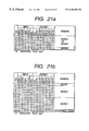
- FIG. 21 a shows a truth table of a control unit (E 1 DEC 1 ) in the first data execution unit
- FIG. 21 b shows a truth table of a control unit (E 2 DEC 1 ) in the second data execution unit;
- FIG. 22 a shows a timing chart of the first data execution unit
- FIG. 22 b shows a timing chart of the second data execution unit
- FIG. 23 shows a second embodiment of the one-chip microcomputer according to the invention.
- FIG. 24 shows a sample of a more specific construction of a mode set circuit (MODE 2 );
- FIG. 25 shows a truth table of a control unit (MDDEC 2 ) in the mode set circuit
- FIG. 26 shows a sample of a more specific construction of a first on-chip memory (MEM 21 );
- FIG. 27 shows a sample of a more specific construction of a first on-chip memory (MEM 22 );
- FIG. 28 shows a truth table of a control unit (MDEC 2 ) in the first on-chip memory in Mode 1 or Mode 3;
- FIG. 29 shows a truth table of the control unit (MDEC 2 ) in the first on-chip memory in Mode 2;
- FIG. 30 shows a truth table of a control unit (MDEC 3 ) in the second on-chip memory in Mode 1 or Mode 3;
- FIG. 31 shows a truth table of the control unit (MDEC 3 ) in the second on-chip memory in Mode 2;
- FIG. 32 shows a sample of a more specific construction of a second data execution unit (EX 22 );
- FIG. 33 shows a truth table of a control unit (E 3 DEC 1 ) in the second data execution unit
- FIG. 34 shows a third embodiment of the one-chip microcomputer according to the invention.
- FIG. 35 shows a sample of a mapping over an address space of first to fourth on-chip memories in Mode 1 and Mode 3;
- FIG. 36 shows a sample of a mapping over an address space of the first to fourth on-chip memories in Mode 2 and for data transfer operations between an on-chip memory and a data execution unit;
- FIG. 37 shows another sample of the mapping over the address space of the first to fourth on-chip memories in Mode 2 and for the data transfer operations between the on-chip memory and the data execution unit;
- FIG. 38 shows a sample of a more specific construction of the first and second on-chip memories (XMEM 1 and XMEM 2 );
- FIG. 39 shows a sample of a more specific construction of the third and fourth on-chip memories (YMEM 1 and YMEM 2 );
- FIG. 40 shows a truth table of a control unit (MDEC 4 ) in the first on-chip memory for an address decoder;
- FIG. 41 shows a truth table of the control unit (MDEC 4 ) in the first on-chip memory in Mode 1;
- FIG. 42 shows a truth table of the control unit (MDEC 4 ) in the first on-chip memory in Mode 2;
- FIG. 43 shows a truth table of the control unit (MDEC 4 ) in the first on-chip memory in Mode 3;
- FIG. 44 shows a truth table of a control unit (MDEC 4 ) in the second on-chip memory for an address decoder;
- FIG. 45 shows a truth table of the control unit (MDEC 4 ) in the second on-chip memory in Mode 1;
- FIG. 46 shows a truth table of the control unit (MDEC 4 ) in the second on-chip memory in Mode 2;
- FIG. 47 shows a truth table of the control unit (MDEC 4 ) in the second on-chip memory in Mode 3;
- FIG. 48 shows a sample of a more specific construction of a first data execution unit (EX 31 );
- FIG. 49 shows a sample of a more specific construction of a second data execution unit (EX 31 );
- FIG. 50 shows a truth table of a control unit (E 4 DEC 1 ) of the first data execution unit
- FIG. 51 shows a truth table of a control unit (E 5 DEC 1 ) of the second data execution unit
- FIG. 52 shows a fourth embodiment of the one-chip microcomputer according to the invention.
- FIG. 53 shows a fifth embodiment of the one-chip microcomputer according to the invention.
- FIG. 54 shows a sixth embodiment of the one-chip microcomputer according to the invention.
- FIG. 55 shows one sample in which an operating mode field is formed in place of the mode set circuit over an instruction code
- FIG. 56 shows a sample of an instruction format and the instruction code
- FIG. 57 shows a sample of the mapping over the address space of the first to fifth on-chip memories in Mode 2 and for the data transfer operations between the on-chip memory and the data execution unit;
- FIG. 58 shows a seventh embodiment of the one-chip microcomputer according to the invention.
- FIG. 1 shows one sample of the block diagram of a one-chip microcomputer according to the invention.
- letters LSI 1 designates a microcomputer according to the invention;
- letters CPU 1 a central processing unit including a circuit for fetching and decoding an instruction to generate a desired control signal;
- letters CFCH 1 an instruction fetch unit included in CPU 1 ;
- letters CDEC an instruction decode unit included in CPU 1 ;
- letters CNT a set of control signals generated by CDEC;
- letters MODE 1 a mode set circuit for setting the microcomputer LSI 1 to a mode, designated by the control signals, to hold the state;
- letters MD[ 1 : 0 ] designates a mode signal for transmitting the present mode state from MODE 1 to a necessary module;
- letters CADR 1 an address generating unit included in CPU 1 for generating the designated address;
- letters IAB an address bus for outputting an address generated in CADR 1 ;
- letters MEM 11 a first on-chip memory packaged over the chip;
- the timer unit TIM the serial interface units SIO 1 and SIO 2 , the external parallel interface unit, the internal control unit IRQ and the data bus for peripheral apparatus will not be detailed in the following description of operations, although they are important components for the microcomputer LSI 1 according to the invention.
- the first data execution unit EX 11 and the second data execution unit EX 12 are functionally equivalent, and their execution functions and the registers in their modules are distinguished not on the instruction code but by the modes.
- the mode set circuit MODE 1 sets one of the following three modes and holds the state.
- the modes may be Mode 1 and Mode 2.
- Mode 1 Can execute a single operation by the first data execution unit. A reset initial value.
- Mode 2 Can execute two parallel operations by the first and second data execution unit.
- Mode 3 Can execute a single operation by the second data execution unit.
- the state signal is encoded and displayed, but it is apparent that the code definitions may be different or that the Modes may be individually displayed with independent state enable signals. Even with the different code definitions and with the Modes being displayed by the independent state enable signals, the first and second data execution units EX 11 and EX 12 may possibly be realized including the control units with the absolutely identical circuit structure, as will be detailed hereinafter.
- FIG. 56 shows a sample of instruction formats and instruction codes, as contained in the instruction set of the microcomputer.
- CPU instructions there are coarsely supported two kinds of instructions, i.e., CPU instructions and DSP instructions. All the CPU instructions and a part of the DSP instructions are instruction codes having a length of 16 bits, and the remaining DSP instructions are instruction codes having a length of 32 bits.
- the CPU instructions are executed exclusively by the CPU core without operating the aforementioned data execution units and execute the same single operation commonly in any Mode.
- the DSP instructions cause the data execution units to execute the operations while causing the CPU core to bear a part of operations such as the address operations or the operand accesses, or execute the data transfer operations with the registers in the data execution units.
- the operations may be executed by the single data execution unit, or the same operations may be executed in parallel by the two data execution units.
- letters nnnn designates a field of a destination operand; letters ssss a field of a source operand; letters dddd a field of a displacement; and letters iiii a field of immediate data.
- the field nnnn is shared with the field of the source operand, and the executed result is stored in the field nnnn.
- These three instructions can be designated by one instruction code and executed in parallel.
- this instruction code more specifically: there are executed in parallel in the data execution units the operations in which the hold data are fed from registers Se and Sf in the data execution units to and operated by a multiplier so that the operated result is written in a register Dg; the operations in which the data designated by an address pointer As are transferred to a destination operand Db; and the operations in which the data designated by an address pointer Pc are transferred to a destination operand Dd.
- the address pointers Aa and Ac are the registers in the CPU core, and the remaining operands are registers in the data execution units.
- a third line is generally identical to the second low but is different in that the instruction “PADD” is replaced by a subtract instruction “PSUB”.
- the sign “+”, as attached to the right of mnemonics (Aa, Ac) of each address pointer designates an operation to update the address at a next memory accessing time by incrementing the pointer after a memory access.
- control has to be made such that the destinations for storing the results of the operations to be executed simultaneously in parallel may not be overlapped.
- an error check may be so software-like performed by an assembler that the operation results may not be stored in a common destination.
- the storing destinations may be overlapped.
- a priority encoder may be employed to give one destination a higher priority while ignoring the other.
- each execution unit is given a construction for executing a single-precision data operation.
- each execution unit can naturally execute both the single-precision data operation and a double-precision data operation.
- a double-precision data operation/double-precision parallel data operations can be executed in addition to the single-precision data operation/single-precision parallel data operations.
- the single-precision data operation and the double-precision data operation may be switched in the Modes.
- FIG. 2 shows a sample of a mapping over the address space of MEM 11 and MEM 12 in Mode 1.
- the memory map of FIG. 2 is identical in Mode 3.
- MEM 11 and MEM 12 are mapped in the continuous address space, but this continuity is not essential. It is needless to say that MEM 11 and MEM 12 may be mapped in an intrinsic address space and that the capacity of each memory should not be fixed at 16 Kbytes.
- the first data execution unit EX 11 is instructed to execute the operations by the control signal which is issued from the central processing unit CPU 1 , but the second data execution unit EX 12 comes into an inactive state independently of the control signal.
- the central processing unit CPU 1 generates a program address in the address generating unit and reads out an instruction from a predetermined memory through IAB and in an instruction code in the instruction fetch unit CFCH 1 from IDB 1 .
- the memory for reading out the instruction need not always be the on-chip memories MEM 11 and MEM 12 , but the instruction may be read in from an external memory through an external parallel interface unit PIO, for example.
- the fetched instruction code is decoded by the instruction decode unit CDEC to generate a set of control signals CNT necessary for the individual modules.
- the address generating unit CADR 1 When the decoded instruction is one for reading out the data from the memories, the address generating unit CADR 1 generates an address to be accessed to and outputs it to the address bus IAB.
- the address thus outputted to IAB is one mapping the on-chip memory MEM 11 or MEM 12 , this MEM 11 or MEM 12 activates a word line of the corresponding address to read out the necessary data and output them to the data bus IDB 1 .
- the data thus outputted to IDB 1 are transferred to the destination operand designated by the instruction.
- the destination operand thus designated by the instruction is a register in the address generating unit CADR 1 , for example, the data are fetched from IDB 1 in CADR 1 and inputted to the predetermined register.
- the operand code is shared between EX 11 and EX 12 .
- the second data execution unit EX 12 is inactive so that the data on IDB 1 are fetched by EX 11 .
- the destination operand designated by the instruction is a register in the mode set circuit MODE 1
- the data are fetched from IDB 1 in MODE 1 to update the predetermined register.
- the mode is switched to that corresponding to a predetermined state.
- the address on IAB is outputted from the parallel interface unit PIO to the outside so that the data read out from the external memory are outputted to IDB 1 through PIO, the data bus PDB for peripheral apparatus and the bus interface unit BIF 1 and are transferred to the destination operand designated by the instruction.
- the address generating unit CADR 1 When the decoded instruction is one for writing the data in the memories, the address generating unit CADR 1 generates an address to be accessed to and outputs it to the address bus IAB. When the address thus outputted to IAB is one mapping the on-chip memory MEM 11 or MEM 12 , this MEM 11 or MEM 12 activates a word line of the corresponding address.
- the source operand thus designated by the instruction is a register in the address generating unit CADR 1 , on the other hand, the data are outputted from CADR 1 to IDB 1 and inputted to the MEM 12 so that they are written at a predetermined address.
- the source operand When the source operand is in the first or second data execution unit EX 11 or EX 12 , the operand code is shared between EX 11 and EX 12 .
- the second data execution unit EX 12 is inactive so that the data in EX 11 are outputted to IDB 1 .
- the source operand designated by the instruction is a register in the mode set circuit MODE 1
- the data are outputted from MODE 1 to IDB 1 .
- the address outputted to IAB is in the field of the external memory
- the address on IAB is outputted from the parallel interface unit PIO to the outside. Simultaneously with this, the data outputted from the source operand to the IDB 1 are written in the external memory through the bus interface unit BIF 1 and the data buses PDB and PIO for the peripheral apparatus.
- mode 1 the data transfer between the individual modules other than the memories is likewise executed by using IDB 1 .
- the second data execution unit EX 12 is inactive so that the first data execution unit EX 11 is automatically accessed to, when the source or destination operand designates the registers or the like in the data execution unit.
- the first on-chip memory MEM 11 , the address generating unit CADR 1 , the instruction fetch unit CFCH 1 , the bus interface BIF 1 and the mode set circuit MODE 1 are controlled to have effective connections with the first data bus IDB 1 .
- the second on-chip memory MEM 12 selects which of the first data bus IDB 1 and the second data bus IDB 2 is to be connected therewith, in accordance with the content of the control received. When this received control is the data transfer operation between the data execution units EX 11 and EX 12 , the second on-chip memory MEM 12 is connected with the second data bus IDB 2 .
- FIG. 3 shows a sample of a mapping over the address space of MEM 11 and MEM 12 at a time of Mode 2 and when the received control is the data transfer operation with the data execution unit EX 11 or EX 12 .
- the case other than that of the time of Mode 2 and when the received control is the data transfer operation with the data execution unit EX 11 or EX 12 is identical to that of FIG. 2 .
- FIG. 3 moreover, there are two double mapping spaces of MEM 11 and MEM 12 . However, it is needless to say that the mapping may be only at one portion, as shown in FIG. 4 .
- the first data execution unit EX 11 and the second data execution unit EX 12 are not distinguished on the instruction code so that they execute the same instruction of the common control signal which is issued from the central processing unit CPU 1 .
- the central processing unit CPU 1 As at the time of Mode 1, the central processing unit CPU 1 generates the program address in the address generating unit, reads out the instruction from the predetermined memory through IAB and reads the instruction code in the instruction fetch unit CFCH 1 from IDB 1 .
- the memory map to be applied is that of FIG. 2 when in the instruction fetch operation, so that the instruction code is correctly read out from the designated address.
- the read instruction code IDB 1 is selected and outputted.
- the fetched instruction code is decoded by the instruction decode unit CDEC to generate the control signal set CNT necessary for the individual modules.
- the operations are identical to those of Mode 1 when the decoded instruction is other than the data transfer operations between the on-chip memories and the data execution units.
- the following operations are executed when the decoded instruction is other than the data transfer operations between the on-chip memories and the data execution units.
- the address generating unit CADR 1 At the time of the instruction to read out the data from the memories, the address generating unit CADR 1 generates an address to be accessed to and outputs it to the address bus IAB.
- the address outputted to IAB activates the word lines at the addresses corresponding to both MEM 11 and MEM 12 to read out the necessary data so that the data read out from the MEM 11 are outputted to the data bus IDB 1 whereas the data read out from the MEM 12 are outputted to the data bus IDB 2 .
- the data outputted to IDB 1 are transferred to the destination operand in the first data execution unit EX 11 designated by the instruction. Simultaneously with this, the data outputted to IDB 2 are transferred to the destination operand in the second data execution unit EX 12 designated by the same instruction.
- the address generating unit CADR 1 At the time of the instruction to write the data in the memories, the address generating unit CADR 1 generates an address to be accessed to, and outputs it to address bus IAB.
- the address outputted to IAB activates simultaneously the word lines of the addresses corresponding to both MEM 11 and MEM 12 .
- the data of the source operand in the first data execution unit EX 11 designated by the instruction are outputted to IDB 1 .
- the data of the source operand in the second data execution unit EX 12 designated by the instruction are outputted to IDB 2 . Since EX 11 and EX 12 are not distinguished on the instruction code, as described hereinbefore, both the operations can be simultaneously executed in Mode 2 with the same instruction code even in response to the data transfer instruction. In the case of the data execution instruction where the resources are closed in the data execution units, it is apparent that a plurality of identical operations can be simultaneously executed with a single instruction code.
- Mode 2 the data transfer between the individual modules other than the memories can be executed between the modules excepting the second data execution unit and is executed by using the first data bus IDB 1 .
- the modules other than the second data execution unit EX 12 are connected with the first data bus IDB 1 , and the operands in the first and second data execution units EX 11 and EX 12 cannot be distinguished with the instruction code. In this Mode, therefore, the data transfer between the modules with the operands in the second data execution unit EX 12 is not supported.
- the access to the operands in the second data execution unit EX 12 is executed, if necessary, by making a switching to Mode 3.
- the second data execution unit EX 12 executes the operations in response to the instruction of the control signal which is issued from the central processing unit CPU 1 , but the first data execution unit EX 11 comes into an inactive state independently of the control signal.
- the central processing unit CPU 1 generates a program address in the address generating unit, reads out the instruction from a predetermined memory through IAB and reads the instruction code in the instruction fetch unit CFCH 1 from IDB 2 .
- the memory for reading out the instruction need not always be the on-chip memories MEM 11 and MEM 12 , but the instruction may be read in from an external memory through an external parallel interface unit PIO, for example.
- the fetched instruction code is decoded by the instruction decode unit CDEC to generate a set of control signals CNT necessary for the individual modules. What is different from Mode 1 is the actions in which the instruction code is read in from the second data bus IDB 2 .
- the address generating unit CADR 1 When the decoded instruction is one for reading out the data from the memories, the address generating unit CADR 1 generates an address to be accessed to and outputs it to the address bus IAB.
- the address thus outputted to IAB is one mapping the on-chip memory MEM 11 or MEM 12 , this MEM 11 or MEM 12 activates a word line of the corresponding address to read out the necessary data and output them to the second data bus IDB 2 .
- the data thus outputted to IDB 2 are transferred to the destination operand designated by the instruction.
- the destination operand thus designated by the instruction is a register in the address generating unit CADR 1 , for example, the data are fetched from IDB 2 in CADR 1 and inputted to the predetermined register.
- the operand code is shared between EX 11 and EX 12 .
- the first data execution unit EX 11 is inactive so that the data on IDB 2 are fetched by EX 12 .
- the destination operand designated by the instruction is a register in the mode set circuit MODE 1
- the data are fetched from IDB 2 in MODE 1 to update the predetermined register.
- the mode is switched to that corresponding to a predetermined state.
- the address on IAB is outputted from the parallel interface unit PIO to the outside so that the data read out from the external memory are outputted to IDB 2 through PIO, the data bus PDB for peripheral apparatus and the bus interface unit BIF 1 and are transferred to the destination operand designated by the instruction.
- the address generating unit CADR 1 When the decoded instruction is one for writing the data in the memories, the address generating unit CADR 1 generates an address to be accessed to and outputs it to the address bus IAB. When the address thus outputted to IAB is one mapping the on-chip memory MEM 11 or MEM 12 , this MEM 11 or MEM 12 activates a word line of the corresponding address.
- the source operand thus designated by the instruction is a register in the address generating unit CADR 1 , on the other hand, the data are outputted from CADR 1 to IDB 2 and inputted to the MEM 12 so that they are written at a predetermined address.
- the source operand When the source operand is in the first or second data execution unit EX 11 or EX 12 , the operand code is shared between EX 11 and EX 12 .
- the first data execution unit EX 11 is inactive so that the data in EX 12 are outputted to IDB 2 .
- the source operand designated by the instruction is a register in the mode set circuit MODE 1
- the data are outputted from MODE 1 to IDB 2 .
- the address outputted to IAB is in the field of the external memory
- the address on IAB is outputted from the parallel interface unit PIO to the outside.
- the data outputted from the source operand to the IDB 2 are written in the external memory through the bus interface unit BIF 1 and the data buses PDB and PIO for the peripheral apparatus.
- mode 3 the data transfer between the individual modules other than the memories is likewise executed by using IDB 2 .
- the first data execution unit EX 11 is inactive so that the second data execution unit EX 12 is automatically accessed to, when the source or destination operand designates the registers or the like in the data execution unit.
- letters MDR designates a mode register constructing bits for holding an MD[ 1 : 0 ] signal indicating a mode state
- letters MDDEC 1 a control unit for generating control signals DCT 1 to DCT 5 in the mode set circuit
- letters DCT 1 to DCT 5 the control signals to be outputted from the control unit MDDEC 1
- letters DMX 1 a selector for selecting and fetching the data on the first data bus IDB 1 or the second data bus IDB 2
- letters DCB 1 a clock gate for inputting the data selected by the selector DMX 1 to a mode register MDR
- letters DLT 1 a delay latch unit for delaying the output signal MD[ 1 : 0 ] of the mode register MDR by a half period
- letters DMX 2 a selector for outputting the output of DLT 1 to the first data bus IDB 1 or the second data bus IDB 2 ;
- DLT 2 a delay latch unit for
- FIG. 6 shows a truth table tabulating the functions of the control unit MDDEC 1
- FIG. 7 shows a timing chart of the mode register at a time of write/read operations.
- the mode set circuit MODE 1 rewrites the content of the mode register MDR to change the state of Mode.
- the mode register MDR indicates the state of Mode 1 corresponding to any of NOs. 1 to 3 of FIG. 6 .
- the central processing unit CPU 1 sets the WTMDR signal to “1”.
- DCT 4 and DCT 5 take the value “1” to input the data, as transferred from the first data bus IDB 1 , to MDR through DMX 1 and DCB 1 .
- the central processing unit CPU 1 sets the RDMDR signal to “1”.
- DCT 2 takes the value “1” so that the content of the MDR register is outputted to the first data bus IDB 1 through DCT 1 and DMX 2 .
- the less significant bits of the data bus i.e., the 0 bit and the 1 bit are employed in FIG. 5 . It is, however, quite natural that the invention should not be limited to those bit positions.
- the operations are similar to those of Mode 1 even if the state is changed to Mode 2 by the preceding writing operation in MDR.
- the second data bus IDB 2 is employed for the input/output of the data in place of the first data bus IDB 1 , and the succeeding operations are identical.
- the input/output data bus can be automatically interchanged in the mode exhibited by the mode register owned by the mode set circuit MODE 1 itself.
- the mode set circuit is exemplified by the independent module. It is, however, apparent that the mode set circuit may be constructed as one register in the central processing unit CPU 1 , for example, and the mode set circuit should not be limited to the manner how to divide the hardware module. Moreover, the mode register MDR is also exemplified by a register dedicated for holding the state of the mode signal MD[ 1 : 0 ]. It is, however, needless to say that the mode register MDR could be constructed as the bits of a part of another control register. It is further apparent that the mode register MDR could be mapped as a memory mapped register.
- the control signals RDMDR and WTMDR to be issued by the central processing unit CPU 1 may be generated as the decoded result of the fetched instruction but may be generated by another method.
- a specific interrupt demand occurs in response to the interrupt request signal IREQ to be outputted from the internal control unit IRQ, for example, there may be provided a function to switch the mode automatically.
- the content of the mode register MDR may be rewritten by the transfer of the data or directly changed in response to a mode set instruction.
- the invention should not be limited to such predetermined specific switching methods. It is, however, apparent that the invention may be provided with the function to set and hold the mode and means for changing the function.
- the instruction fetch unit CFCH 1 or the address generating unit CADR 1 in the central processing unit CPU 1 can be automatically controlled from either the first data bus IDB 1 or the second data bus IDB 2 by a construction method similar to that of the mode set circuit MDDEC 1 .
- a fetch is an operation to write in the fetch register, and a fetch control signal may be used in place of the control signal RDMDR.
- the fetch unit need not be provided with the read function.
- the address generating unit is usually realized by using a general purpose register and an arithmetic logic unit.
- the switching control method of the data bus in the data transfer between the register in the address generating unit and the data bus is similar to the mode set circuit MDDEC, and the remaining intrinsic operations of the address generating unit are not different from the ordinary ones so that their detailed description will be omitted.
- FIG. 8 A sample of a more specific construction of the first or second on-chip memory MEM 11 or MEM 12 is shown in FIG. 8 .
- letters MADC designates an address decoder
- letters M 0 , M 1 , M 2 and M 3 memory mats for storing data at the unit of 1 byte, respectively
- letters MLT 0 , MLT 1 , MLT 2 and MLT 3 latch units for relaying the inputs/outputs of data at the byte unit, respectively, with the memory mats
- letters MLT 4 a latch unit for fetching the information of less significant 15 bits of the address bus IAB in the first on-chip memory MEM 11 ;
- MMX 1 , MMX 3 , MMX 5 , MMX 6 , MMX 7 and MMX 8 selectors for selecting and outputting one of plural inputs;
- the structures of the first and second on-chip memories are identical excepting that the truth tables of the control units are different.
- the memories to be described distinguish three types of data lengths in response to an instruction so that a memory having a corresponding function is taken up.
- the corresponding relations between the addresses and the actual memories are shown in FIG. 9 .
- the memory mats M 0 , M 1 , M 2 and M 3 store data of the unit of 1 byte and correspond to the addresses 4 n, 4 n+1, 4 n+2 and 4 n+3 (n: an integer no less than 0).
- the central processing unit CPU 1 can designate an arbitrary address.
- the letters ML[ 1 : 0 ] designates a code for enabling a word line of 1 byte
- the address decoder MADC enables the word line of the memory mat corresponding to the address designated by [ 13 : 0 ] of MLT 4 .
- the central processing unit CPU 1 designates the address 4 n or 4 n+2.
- the letters ML[ 1 : 0 ] designates a code for enabling the word lines of consecutive 2 bytes, and the address decoder MADC enables the word lines of two memory mats at the address 4 n, as designated by [ 13 : 0 ] of MLT 4 and the subsequent 4 n+1, or 4 n+2 and the subsequent 4 n+3.
- the central processing unit CPU 1 designates the address 4 n.
- the letters ML[ 1 : 0 ] designates a code for enabling the word lines of consecutive 4 bytes, and the address decoder MADC enables the word lines of all the four memory mats at the address 4 n, as designated by [ 13 : 0 ] of MLT 4 and the subsequent 4 n+1, 4 n+2 and 4 n+3.
- the control code signal MV[ 2 : 0 ] is a code signal, as defined in FIG. 10 .
- the code signal supports three kinds of data transfer operations of a byte unit, a word unit and a long word unit in the case of the data transfer operations of the on-chip memories with the exception of the first and second data execution units.
- the sample supports two kinds of the data transfer operations of the word unit and the long word unit, but can naturally support three kinds.
- the MSEL is the memory access enable signal shared among the on-chip memories and is generated to omit the means for decoding the more significant information of the addresses with the individual on-chip memories.
- the individual on-chip memories can be distinguished therein with the 15th (IAV[ 14 ]) of IAB and the information of the mode state signal MD[ 1 : 0 ] because they have a capacity of 16 Kbytes.
- the control signal WE designates the read operation or the write operation.
- the low state implies the read operation whereas the high state implies the write operation.
- the signal MV[ 2 : 0 ] designates the memory access operations for the instruction fetch operation, the data transfer operations with the exception of the data execution units and the data transfer operations with the data execution units and is defined with different codes according to the bit width of the data to be accessed to.
- the microcomputer LSI is assumed to execute the fixed length instruction fetch operation of 32 bits. As shown in FIG. 10, therefore, the instruction fetch operation is defined by one kind of code.
- FIG. 11, FIG. 12 and FIG. 13 show truth tables of the definitions of the control unit MDEC 1 in Mode 1, Mode 2 and Mode 3, respectively.
- the truth table is shown in each Mode, but one table is too large to present so that it is divided.
- this truth table is such a logic unit as can be presented in one table by adding MD[ 1 : 0 ] to the input signal, as shown in FIG. 6 .
- the truth tables of FIGS. 11, 12 and 13 anticipate the memory map of FIG. 3 .
- the unused codes are filled in such rows for simplicity as are expected to have less hardware.
- FIG. 14 shows a timing chart of the first on-chip memory MEM 11 exemplifying the read/write operations of the data at the long word unit.
- the second on-chip memory MEM 12 has an identical timing although the data buses to be connected are different for the Modes.
- the memory unit In order to time the read and write memory mats, the memory unit is different from the read/write timings in the preceding mode set register. However, the timing itself is determined as the specifications in the microcomputer providing the base.
- the individual operations for the different Modes are described.
- the AS signal comes into the enable state (high), and ML[ 1 : 0 ] indicates the code (11) for enabling the word liens of four consecutive bytes so that the addresss decoder MADC reads out the data by enabling the predetermined word lines of all the four memory mats.
- the data thus read out are latched by the latch units MLT 0 to MLT 3 .
- the data, as latched by MLT 0 pass through the selector MMX 1 with MCT 4 being enabled and further through the selector MMX 9 with MCT 16 being enabled so that they are outputted to the least significant byte ([ 7 : 0 ]) of the first data bus IDB 1 .
- the data as latched by MLT 3 , pass through the selector MMX 12 with MCT 20 being enabled so that they are outputted to the most significant byte ([ 31 : 24 ]) of the first data bus IDB 1 .
- the detailed control signals and circuit constructions of the latch units MLT 0 to MLT 3 , the address decoder MADC and the memory mats M 0 to M 3 have no direct relation to the invention, but this memory unit having a variable data length and a memory accessibility is known in the prior art so that its direction will be omitted, as in the following description.
- the data, thus read out, are latched by the latch units MLT 0 , MLT 1 , MLT 2 or MLT 3 connected with the accessed memory mat.
- the data, as read out from the memory mat M 0 are latched by MLT 0 and pass through the selector MMX 1 with MCT 4 being enabled and further through the selector MMX 9 with MCT 16 being enabled, so that they are outputted to the least significant byte ([ 7 : 0 ]) of the first data bus IDB 1 .
- the data When the less significant 2 bits of the address information latched by MLT 4 are 01, the data, as read out from the memory mat M 1 , are latched by MLT 1 and pass through the selector MMX 1 with MCT 3 being enabled and further through the selector MMX 9 with MCT 16 being enabled, so that they are outputted to the least significant byte ([ 7 : 0 ]) of the first data bus IDB 1 .
- the data As read out from the memory mat M 2 , latched by MLT 2 and pass through the selector MMX 1 with MCT 2 being enabled and further through the selector MMX 9 with MCT 16 being enabled, so that they are outputted to the least significant byte ([ 7 : 0 ]) of the first data bus IDB 1 .
- the data As read out from the memory mat M 3 , latched by MLT 3 and pass through the selector MMX 1 with MCT 1 being enabled and further through the selector MMX 9 with MCT 16 being enabled, so that they are outputted to the least significant byte ([ 7 : 0 ]) of the first data bus IDB 1 .
- the byte data of an arbitrary address are outputted to the least significant byte of the first data bus IDB 1 .
- the data to be written are sent as at the read time from the least significant byte of the first data bus IDB 1 .
- MSEL exhibits the enable state
- the first on-chip memory MEM 11 executes the write operation of the data at the byte unit.
- the AS signal comes into the enable state (high)
- ML[ 1 : 0 ] indicates the code (01) for enabling the word line of 1 byte, so that the address decoder MADC writes the data in the latch unit by enabling a predetermined word line of one corresponding memory mat.
- the data When the lest significant 2 bits of the address information latched by MLT 4 is 00, the data, as sent from the least significant byte of the first data bus IDB 1 , pass through the selector MMX 5 with MCT 15 being enabled and further through the selector MMX 2 with MCT 5 being enabled, so that they are inputted to MLT 0 and written in the memory mat M 0 .
- the data When the less significant 2 bits of the address information latched by MLT 4 is 01, the data, as sent from the least significant byte of the first data bus IDB 1 , likewise pass through the selector MMX 5 with MCT 15 being enabled and further through the selector MMX 2 with MCT 6 being enabled, so that they are inputted to MLT 1 and written in the memory mat M 1 .
- the data when the less significant 2 bits of the address information latched by MLT 4 is 10, the data, as sent from the least significant byte of the first data bus IDB 1 , likewise pass through the selector MMX 5 with MCT 15 being enabled and further through the selector MMX 2 with MCT 7 being enabled, so that they are inputted to MLT 2 and written in the memory mat M 2 .
- the data when the less significant 2 bits of the address information latched by MLT 4 is 11, the data, as sent from the least significant byte of the first data bus IDB 1 , likewise pass through the selector MMX 5 with MCT 15 being enabled and further through the selector MMX 2 with MCT 8 being enabled, so that they are inputted to MLT 3 and written in the memory mat M 3 .
- the data, thus read out, are latched by the latch units MLT 0 and MLT 1 or MLT 2 and MLT 3 , as connected with the accessed memory mats.
- the data, as read out from the memory mats M 0 and M 1 are latched by MLT 0 and MLT 1 and pass through the selectors MMX 1 and MMX 3 with MCT 4 and MCT 10 being enabled and further through the selectors MMX 9 and MMX 10 with MCT 16 and MCT 18 being enabled, so that they are outputted to the less significant 2 bytes ([ 15 : 0 ]) of the first data bus IDB 1 .
- the data As read out from the memory mats M 2 and M 3 , are latched by MLT 2 and MLT 3 and pass through the selectors MMX 1 and MMX 3 with MCT 4 and MCT 10 being enabled and further through the selectors MMX 9 and MMX 10 with MCT 16 and MCT 18 being enabled, so that they are outputted to the less significant 2 bytes ([ 15 : 0 ]) of the first data bus IDB 1 .
- the data to be written are sent as at the read time from the less significant 2 bytes of the first data bus IDB 1 .
- MSEL exhibits the enable state
- the first on-chip memory MEM 11 executes the write operation of the data at the word unit.
- the AS signal comes into the enable state (high)
- ML[ 1 : 0 ] indicates the code (10) for enabling the word lines of 2 bytes, so that the address decoder MADC writes the data in the corresponding latch unit by enabling the predetermined word lines of the corresponding consecutive two memory mats.
- the data As sent from the less significant 2 bytes of the first data bus IDB 1 , pass through the selectors MMX 5 and MMX 6 with MCT 15 being enabled and further through the selectors MMX 2 and MMX 4 with MCT 5 and MCT 11 being enabled, so that they are inputted to MLT 0 and MLT 1 and written in the memory mats M 0 and M 1 .
- the data As sent from the less significant 2 bytes of the first data bus IDB 1 , pass through the selectors MMX 5 and MMX 6 with MCT 15 being enabled and further through the selectors MMX 2 and MMX 4 with MCT 7 and MCT 12 being enabled, so that they are inputted to MLT 2 and MLT 3 and written in the memory mats M 2 and M 3 .
- the data as read out from the memory mats M 0 to M 3 , are latched by MLT 0 to MLT 3 and pass through the selectors MMX 1 and MMX 3 with MCT 4 and MCT 10 being enabled and further through the selectors MMX 9 , MMX 10 , MMX 11 and MMX 12 with MCT 16 , MCT 18 and MCT 20 being enabled, so that they are outputted to the first data bus IDB 1 ([ 31 : 0 ]).
- the data to be written are sent as at the read time by using all the bits of the first data bus IDB 1 .
- MSEL exhibits the enable state
- the first on-chip memory MEM 11 executes the write operation of the data at the long word unit.
- the AS signal comes into the enable state (high)
- ML[ 1 : 0 ] indicates the code for enabling the word lines of 4 bytes, so that the address decoder MADC writes the data in the corresponding latch unit by enabling the predetermined word lines of all the four memory mats.
- the data as sent from the first data bus IDB 1 , pass through the selectors MMX 5 , MMX 6 , MMX 7 and MMX 8 with the MCT 15 being enabled and further through MMX 2 , MMX 4 , MCB 1 and MCB 2 with MCT 5 , MCT 11 and MCT 13 being enabled, so that they are inputted to MLT 0 to MLT 3 and written in the memory mats M 0 to M 3 .
- the data, as latched by MLT 1 pass through the selector MMX 3 with MCT 10 being enabled and further through the selector MMX 10 with MCT 19 being enabled so that they are outputted to the second byte ([ 15 : 8 ]) from the least significant byte of the second data bus IDB 2 .
- the data, thus read out, are latched by the latch units MLT 0 , MLT 1 , MLT 2 or MLT 3 connected with the accessed memory mat.
- the data, as read out from the memory mat M 0 are latched by MLT 0 and pass through the selector MMX 1 with MCT 4 being enabled and further through the selector MMX 9 with MCT 17 being enabled, so that they are outputted to the least significant byte ([ 7 : 0 ]) of the second data bus IDB 2 .
- the data When the less significant 2 bits of the address information latched by MLT 4 are 01, the data, as read out from the memory mat M 1 , are latched by MLT 1 and pass through the selector MMX 1 with MCT 3 being enabled and further through the selector MMX 9 with MCT 17 being enabled, so that they are outputted to the least significant byte ([ 7 : 0 ]) of the second data bus IDB 2 .
- the data As read out from the memory mat M 2 , latched by MLT 2 and pass through the selector MMX 1 with MCT 2 being enabled and further through the selector MMX 9 with MCT 17 being enabled, so that they are outputted to the least significant byte ([ 7 : 0 ]) of the second data bus IDB 2 .
- the data As read out from the memory mat M 3 , latched by MLT 3 and pass through the selector MMX 1 with MCT 1 being enabled and further through the selector MMX 9 with MCT 17 being enabled, so that they are outputted to the least significant byte ([ 7 : 0 ]) of the second data bus IDB 2 .
- the byte data of an arbitrary address are outputted to the least significant byte of the second data bus IDB 2 .
- the data to be written are sent as at the read time from the least significant byte of the second data bus IDB 2 .
- MSEL exhibits the enable state
- the first on-chip memory MEM 11 executes the write operation of the data at the byte unit.
- the AS signal comes into the enable state (high)
- ML[ 1 : 0 ] indicates the code (01) for enabling the word line of 1 byte, so that the address decoder MADC writes the data in the latch unit by enabling a predetermined word line of one corresponding memory mat.
- the data When the less significant 2 bits of the address information latched by MLT 4 is 00, the data, as sent from the least significant byte of the second data bus IDB 2 , pass through the selector MMX 5 with MCT 14 being enabled and further through the selector MMX 2 with MCT 5 being enabled, so that they are inputted to MLT 0 and written in the memory mat M 0 .
- the data when the less significant 2 bits of the address information latched by MLT 4 is 01, the data, as sent from the least significant byte of the second data bus IDB 2 , likewise pass through the selector MMX 5 with MCT 14 being enabled and further through the selector MMX 2 with MCT 6 being enabled, so that they are inputted to MLT 1 and written in the memory mat M 1 .
- the data when the less significant 2 bits of the address information latched by MLT 4 is 10, the data, as sent from the least significant byte of the second data bus IDB 2 , likewise pass through the selector MMX 5 with MCT 14 being enabled and further through the selector MMX 2 with MCT 7 being enabled, so that they are inputted to MLT 2 and written in the memory mat M 2 .
- the data when the less significant 2 bits of the address information latched by MLT 4 is 11, the data, as sent from the least significant byte of the second data bus IDB 2 , likewise pass through the selector MMX 5 with MCT 14 being enabled and further through the selector MMX 2 with MCT 8 being enabled, so that they are inputted to MLT 3 and written in the memory mat M 3 .
- the data, thus read out, are latched by the latch units MLT 0 and MLT 1 or MLT 2 and MLT 3 , as connected with the accessed memory mats.
- the data, as read out from the memory mats M 0 and M 1 are latched by MLT 0 and MLT 1 and pass through the selectors MMX 1 and MMX 3 with MCT 4 and MCT 10 being enabled and further through the selectors MMX 9 and MMX 1 O with MCT 17 and MCT 18 being enabled, so that they are outputted to the less significant 2 bytes ([ 15 : 0 ]) of the second data bus IDB 2 .
- the data As read out from the memory mats M 2 and M 3 , are latched by MLT 2 and MLT 3 and pass through the selectors MMX 1 and MMX 3 with MCT 4 and MCT 10 being enabled and further through the selectors MMX 9 and MMX 10 with MCT 17 and MCT 19 being enabled, so that they are outputted to the less significant 2 bytes ([ 15 : 0 ]) of the second data bus IDB 2 .
- the data to be written are sent as at the read time from the less significant 2 bytes of the second data bus IDB 2 .
- MSEL exhibits the enable state
- the first on-chip memory MEM 11 executes the write operation of the data at the word unit.
- the AS signal comes into the enable state (high)
- ML[ 1 : 0 ]) indicates the code (10) for enabling the word lines of 2 bytes, so that the address decoder MADC writes the data in the corresponding latch unit by enabling the predetermined word lines of the corresponding consecutive two memory mats.
- the data As sent from the less significant 2 bytes of the second data bus IDB 2 , pass through the selectors MMX 5 and MMX 6 with MCT 14 being enabled and further through the selectors MMX 2 and MMX 4 with MCT 5 and MCT 11 being enabled, so that they are inputted to MLT 0 and MLT 1 and written in the memory mats M 0 and M 1 .
- the data As sent from the less significant 2 bytes of the second data bus IDB 2 , pass through the selectors MMX 5 and MMX 6 with MCT 14 being enabled and further through the selectors MMX 2 and MMX 4 with MCT 7 and MCT 12 being enabled, so that they are inputted to MLT 2 and MLT 3 and written in the memory mats M 2 and M 3 .
- the data as read out from the memory mats M 0 to M 3 , are latched by MLT 0 to MLT 3 and pass through the selectors MMX 1 and MMX 3 with MCT 4 and MCT 10 being enabled and further through the selectors MMX 9 , MMX 10 , MMX 11 and MMX 12 with MCT 17 , MCT 19 and MCT 21 being enabled, so that they are outputted to the second data bus IDB 2 ([ 31 : 0 ]).
- the data to be written are sent as at the read time by using all the bits of the second data bus IDB 2 .
- MSEL exhibits the enable state
- the first on-chip memory MEM 11 executes the write operation of the data at the long word unit.
- the AS signal comes into the enable state (high)
- ML[ 1 : 0 ] indicates the code for enabling the word lines of 4 bytes, so that the address decoder MADC writes the data in the corresponding latch unit by enabling the predetermined word lines of all the four memory mats.
- the data as sent from the second data bus IDB 2 , pass through the selectors MMX 5 , MMX 6 , MMX 7 and MMX 8 with the MCT 14 being enabled and further through MMX 2 , MMX 4 , MCB 1 and MCB 2 with MCT 5 , MCT 11 and MCT 13 being enabled, so that they are inputted to MLT 0 to MLT 3 and written in the memory mats M 0 to M 3 .
- This second on-chip memory MEM 12 is a memory like MEM 11 having a function to correspond three types of data lengths separately in response to an instruction.
- the corresponding relations the addresses and the actual memories in the second on-chip memory MEM 12 are shown in FIG. 15 .
- FIG. 16, FIG. 17 and FIG. 18 show truth tables of the control unit MDEC 1 in the second on-chip memory MEM 12 in Mode 1, Mode 2 and Mode 3, respectively.
- the truth tables of FIGS. 16, 17 and 18 anticipate the memory mat of FIG. 3 .
- the individual operations separately in different Modes.
- the second on-chip memory MEM 12 executes the read operation of the data of a long word (of 32 bits). The subsequent operations are identical to those of the first on-chip memory MEM 11 .
- the second on-chip memory MEM 12 executes the read operation the data at the byte unit.
- the subsequent operations are identical to those of the first on-chip memory MEM 11 .
- the data to be written are sent as at the read time from the least significant byte of the first data bus IDB 1 .
- MSEL exhibits the enable state
- the second on-chip memory MEM 12 executes the write operation the data at the byte unit.
- the subsequent operations are identical to those of the first on-chip memory MEM 11 .
- the second on-chip memory MEM 12 executes the read operation the data at the word unit.
- the subsequent operations are identical to those of the first on-chip memory MEM 11 .
- the data to be written are sent as at the read time from two less significant bytes of the first data bus IDB 1 .
- MSEL exhibits the enable state
- the second on-chip memory MEM 12 executes the write operation the data at the word unit.
- the subsequent operations are identical to those of the first on-chip memory MEM 11 .
- the second on-chip memory MEM 12 executes the read operation the data at the long word unit.
- the subsequent operations are identical to those of the first on-chip memory MEM 11 .
- the data to be written are sent as at the read time by using all bits of the first data bus IDB 1 .
- MSEL exhibits the enable state
- the second on-chip memory MEM 12 executes the write operation the data at the long word unit.
- the subsequent operations are identical to those of the first on-chip memory MEM 11 .
- the second on-chip memory MEM 12 executes the read operation of the data at the word unit.
- MV[ 2 : 0 ] designates the code indicating the read operation of the data for the data transfer with the exception of the data execution unit
- the read operation is identical to the aforementioned case of (6) Read operation of Data at Long Word Unit in Mode 1, if the 15th bit (IAB[ 14 ]) of IAB is high.
- the first on-chip memory MEM 11 executes the data read operation of the long word (of 32 bits). The subsequent operations are identical to those of the first on-chip memory MEM 1 .
- the second on-chip memory MEM 12 executes the read operation of the data at the byte unit.
- the subsequent operations are identical to those of the first on-chip memory MEM 11 .
- the data to be written are sent as at the read time from the least significant byte of the second data bus IDB 2 .
- MSEL exhibits the enable state
- the second on-chip memory MEM 12 executes the write operation of the data at the byte unit.
- the subsequent operations are identical to those of the first on-chip memory MEM 11 .
- the second on-chip memory MEM 12 executes the read operation of the data at the word unit.
- the subsequent operations are identical to those of the first on-chip memory MEM 11 .
- the data to be written are sent as at the read time from the less significant 2 bytes of the second data bus IDB 2 .
- MSEL exhibits the enable state
- the second on-chip memory MEM 12 executes the write operation of the data at the word unit.
- the subsequent operations are identical to those of the first on-chip memory MEM 1 .
- the second on-chip memory MEM 12 executes the read operation of the data at the long word unit.
- the subsequent operations are identical to those of the first on-chip memory MEM 1 .
- the data to be written are sent as at the read time by using all the bits of the second data bus IDB 2 .
- MSEL exhibits the enable state
- the second on-chip memory MEM 12 executes the write operation of the data at the long word unit.
- the subsequent operations are identical to those of the first on-chip memory MEM 11 .
- FIG. 19 A sample of a more specific construction of the first data execution unit EX 11 is shown in FIG. 19 .
- letters ERG designates a register file in the first data execution unit EX 11 ; letters EMPY an execution unit for multiplier; letters EALU an arithmetic logic unit; letters E 1 DEC 1 a control unit for generating data transfer control signals ECT 1 to ECT 6 in the first data execution unit EX 11 ; letters EDEC 2 a control unit for generating a set of data execution control signals ERGCT, EMTCT and EALCT in the first data execution unit EX 11 ; letters ECT 1 to ECT 6 the control signals to be outputted from the control unit E 1 DEC 1 ; letters EMX 1 a selector for selecting and fetching a more significant word (of 16 bits) or a less significant word of the first data bus IDB 1 ; letters EMX 2 a selector for selecting and fetching the less significant words (of 16 bits) or all zero data of the first data bus IDB 1 ;
- the set control signals ERGCT for the data execution are composed of a plurality of kinds of signals including: the signals for selecting a specific register such as R 0 H or R 1 L in the register file ERG and for feeding the held data to the execution unit for the multiplier; the signals for selecting a specific register such as R 1 H or RQL in the register file ERG and for feeding the held data to the arithmetic logic unit EALU; and the control signals for storing the executed result coming from the execution unit for the multiplier EMPY or the arithmetic logic unit EALU in the selected register such as R 2 H or R 2 L.
- the set control signals EMTCT for the data transfer for the data transfer are composed of a plurality of kinds of signals including: the signals for designating whether or not the input data to be fed to the execution unit for the multiplier EMPY are signed; and the signals for determining whether or not the executed result of the execution unit for the multiplier EMPY is to be shifted.
- the set control signals EALCT for the data transfer are composed of a plurality of kinds of signals such as signals for selecting the arithmetic executions such as AND, OR, Exclusive OR in the arithmetic logic unit EALU.
- FIG. 20 A sample of a more specific construction of the second data execution unit EX 12 is shown in FIG. 20 .
- the first and second data execution units EX 11 and EX 12 are identical in structures excepting the truth tables defining the functions the data buses and the control units E 1 DEC 1 and E 2 DEC 1 to be connected, and their reference numerals and their descriptions are omitted.
- FIG. 21 a shows a truth table enumerating the functions of the control unit E 1 DEC 1
- FIG. 22 a is a timing chart of the register file in the first data execution unit EX 11 at the time of the write/read operations.
- the data execution unit of this embodiment takes an execution unit capable of executing the digital signal processing efficiently.
- the register file ERG is constructed of a plurality of registers having a length of 32 bits. Each register is constructed of more significant words having a length of 16 bits and less significant words having a length of 16 bits. For example, the register R 0 is composed of a more significant word R 0 H and a less significant word R 0 L.
- the execution unit there are mounted the ordinary arithmetic logic unit EALU and the execution unit for the multiplier EMPY, which are so controlled by the set control signals EXCNT that they can be arithmetically executed in parallel.
- the arithmetic logic unit EALU executes the operations of the same 32 bits as the bit length of the register.
- the execution unit for the multiplier receives the data of 16 bits as its source data to output the result of 32 bits.
- the data execution control unit EDEC 2 may come into the state capable of generating the set control signals for the data execution ERGCT, EMTCT and EALCT, it receives an operation enable signal EN from the control unit E 1 DEC 1 .
- the data execution control unit EDEC 2 having received the execution enable signal EN selects a specific register in the register file ERG of the set control signals ERGCT for the data execution.
- one input of the multiplier EMPY has a bit length of 16 bits so that the register of 16 bits is selected as a multiplier R 0 H and a multiplicand R 3 H.
- To ERG there is fed the signal for feeding the data, as held in the selected register of 16 bits, to the multiplier EMPY.
- the EDEC 2 feeds the multiplier EMPY of the set control signals EMTCT for the data execution with the signal designating whether or not the fed input data are signed or the signal for determining whether the execution result of the multiplier EMPY is to be shifted, thereby to cause the multiplier EMPY to execute operation designated by EMTCT.
- the result of the execution is designated to the specific register in the register file ERG.
- the output of the multiplier EMPY has a bit length of 32 bits so that one register such as R 2 H or R 2 L is selected.
- the control signal for writing the result of the execution in the designated register is fed from the data execution control unit EDEC 2 to the register file ERG. In response to the control signal, the result of the execution in the multiplier EMPY is written in the specific register in the register file ERG.
- the data execution control unit EDEC 2 may come into the state capable of generating the set control signals for the data execution ERGCT, EMTCT and EALCT, it receives an operation enable signal EN from the control unit E 1 DEC 1 . This point is identical to that of the aforementioned operation of the multiplier.
- the data execution control unit EDEC 2 having received the execution enable signal EN selects a specific register in the register file ERG of the set control signals ERGCT for the data execution.
- one input of the arithmetic LOGIC unit EALU has a bit length of 32 bits so that one register such as R 0 h and R 0 L, and R 1 H and R 1 L is selected.
- To ERG there is fed the signal for feeding the data, as held in the selected register, to the arithmetic LOGIC unit EALU.
- the EDEC 2 feeds the arithmetic LOGIC unit EALU of the set control signals EALCT for the data execution with the signal for selecting the arithmetic logic operations such as ADD, AND, OR or Exclusive OR, thereby to cause the arithmetic logic unit EALU to execute operation designated by EALCT.
- the result of the execution is designated to the specific register in the register file ERG.
- the output of the arithmetic LOGIC unit EALU has a bit length of 32 bits so that one register of 32 bits is designated.
- the control signal for writing the result of the execution in the designated register is fed from the data execution control unit EDEC 2 to the register file ERG.
- the result of the execution in the arithmetic LOGIC unit EALU is written in the specific register in the register file ERG.
- the multiply and accumulation operation is executed in a filtering operation.
- the result of the operation is employed as one input of the arithmetic logic unit EALU for the arithmetic logic operation.
- the pipe-line operation i.e., the operation in the multiplier and the operation to execute the operation result of one cycle before in the multiplier as one input of the arithmetic logic unit.
- the description of the operation of the multiplier EMPY and the description of the operation of the arithmetic logic unit EALU thus far made are similar in another embodiment. It is needless to say that the multiply and accumulation operation to be executed in the filtering operation can also be realized in another embodiment by combining the operation in the multiplier and the operation in the arithmetic logic unit.
- the “inactive state” of an execution unit implies the state in which no data transfer is between the data execution unit and the data bus.
- the data to be fed to a second execution unit are in the first data bus, for example, the data are broken if the data from the first execution unit are transferred to the first data bus. Therefore, the data execution unit in the “inactive state” is required at least not to transfer the data to the data bus.
- control unit E 1 DEC 1 having received the set control signals of the data execution unit is active, but the output of the data from the register file ERG to the data bus is interrupted by fixing the signals to be outputted from the control unit E 1 DEC 1 , in the low state, i.e., in the disable state thereby to disconnect the clocked gate ECB 3 and the selector EMX 3 controlling the data output to the data bus.
- the clocked gate ECB 3 and the selector EMX 3 are disconnected by taking a timing with a clock CK 1 or CK 2 on the basis of the signal ECT 3 and ECT 4 .
- the clocked gates ECB 1 to ECB 3 and EMX 3 can also be disconnected to interrupt the output of the data from the register file ERG to the data bus.
- the input to the register file ERG can naturally be interrupted.
- the signals ECT 1 , ECT 2 and ECT 5 may be fixed in the disable state.
- the input from the data bus can naturally be interrupted by fixing the clock signals CK 1 and CK 2 in the disable state.
- the operations may be interrupted by inputting the operation enable signal EN from the control unit E 1 DEC 1 to the data execution control unit EDEC 2 to invite no transition of the state of the multiplier EMPY and the arithmetic logic unit EALU.
- execution units and registers handle at least the data of fixed point type.
- the detailed description of the method for handling the integer data and the fixed point data is omitted because so many samples are already in the prior art. However, here will be described a difference at the time of the data transfer which has a deep relation to the practice of the invention.
- the operations are identical to those which are executed by the CPU of the microcomputer of the prior art.
- word data having a length of 16 bits are to be transferred, more specifically, what is to be transferred is the less significant 16 bits of the register. Since the decimal point is located in the case of the fixed point data between a bit 31 and a bit 30 , on the other hand, the less significant side is so far lighter than the more significant side as to fall within an error range as the case may be.
- data having a smaller width than the bit length of the register are to be transferred, therefore, the more significant data are to be transferred. In this embodiment, too, the more significant register is to be subjected to the transfer in the case of the data transfer of a word length (of 16 bits).
- the control signal ECT 2 is enabled, the word data at the less significant 16 bits of the first data bus IDB 1 pass through the selector EMX 1 and further through the clocked gate ECB 1 with ECT 5 being enabled, and are fetched by the register file ERG so that they are inputted to the more significant words of the designated destination register. Simultaneously with this, all zero data are outputted from the selector EMX 2 and are fetched through the clocked gate ECB 2 by the register file ERG so that they are inputted to the less significant words of the designated destination register.
- the control signal ECT 6 When the control signal ECT 6 is enabled, the data to be outputted pass from the more significant words of the source register in the register file ERG through the latch unit ELT 1 and further through the selector EMX 3 with the ECT 4 being enabled, and are outputted to the less significant 16 bits of the first data bus IDB 1 .
- the control signal ECT 2 is enabled, the word data at the more significant 16 bits of the first data bus IDB 1 pass through the selector EMX 1 and further through the clocked gate ECB 1 with ECT 5 being enabled, and are fetched by the register file ERG so that they are inputted to the more significant words of the designated destination register.
- the word data at the less significant 16 bits of the first data bus IDB 1 are inputted from the selector EMX 2 and are fetched through the clocked gate ECB 2 by the register file ERG so that they are inputted to the less significant words of the designated destination register.
- the control signal ECT 3 When the control signal ECT 3 is enabled, the data to be outputted pass from the more significant words of the source register in the register file ERG through the latch unit ELT 1 and further through the selector EMX 3 with the ECT 4 being enabled, and are outputted to the more significant 16 bits of the first data bus IDB 1 .
- the data to be outputted pass from the less significant words of the source register in the register file ERG through the latch unit ELT 2 and further through the clocked gate ECB 3 and are outputted to the less significant 16 bits of the first data bus IDB 1 .
- the control unit E 1 DEC 1 disables the operation enable signal EN. From now on, the first data execution unit EX 11 will not execute the operation but hold the disable state till the Mode is changed, no matter what operation is instructed by the central processing unit CPU 1 . In this mode, the control issued by the central processing unit CPU 1 is effective in the second data execution unit EX 12 .
- FIG. 21 b shows a truth table enumerating the functions of the control unit E 2 DEC 1 .
- the timing is identical to that of the first data execution unit EX 11 .
- the control unit E 2 DEC 1 disables the operation enable signal EN. From now on, the second data execution unit EX 12 will not execute the operation but hold the disable state till the Mode is changed, no matter what operation is instructed by the central processing unit CPU 1 . In this mode, the control issued by the central processing unit CPU 1 is effective in the first data execution unit EX 11 .
- the control signal ECT 2 is enabled, the word data at the less significant 16 bits of the second data bus IDB 2 pass through the selector EMX 1 and further through the clocked gate ECB 1 with ECT 5 being enabled, and are fetched by the register file ERG so that they are inputted to the more significant words of the designated destination register. Simultaneously with this, all zero data are outputted from the selector EMX 2 and are fetched through the clocked gate ECB 2 by the register file ERG so that they are inputted to the less significant words of the designated destination register.
- the control signal ECT 6 When the control signal ECT 6 is enabled, the data to be outputted pass from the more significant words of the source register in the register file ERG through the latch unit ELT 1 and further through the selector EMX 3 with the ECT 4 being enabled, and are outputted to the less significant 16 bits of the second data bus IDB 2 .
- the control signal ECT 2 is enabled, the word data at the more significant 16 bits of the second data bus IDB 2 pass through the selector EMX 1 and further through the clocked gate ECB 1 with ECT 5 being enabled, and are fetched by the register file ERG so that they are inputted to the more significant words of the designated destination register.
- the word data at the less significant 16 bits of the second data bus IDB 2 are inputted from the selector EMX 2 and are fetched through the clocked gate ECB 2 by the register file ERG so that they are inputted to the less significant words of the designated destination register.
- the control signal ECT 3 When the control signal ECT 3 is enabled, the data to be outputted pass from the more significant words of the source register in the register file ERG through the latch unit ELT 1 and further through the selector EMX 3 with the ECT 6 being enabled, and are outputted to the more significant 16 bits of the second data bus IDB 2 .
- the data to be outputted pass from the less significant words of the source register in the register file ERG through the latch unit ELT 2 and further through the clocked gate ECB 3 and are outputted to the less significant 16 bits of the second data bus IDB 2 .
- the source data necessary for the operations can be supplied without delay to sufficiently exhibit the effect of a high performance by the two parallel execution function in response to the single instruction without being obstructed by the data transfer. Moreover, no problem arises in the consistency with the ordinary single operation.
- control unit E 1 DEC 1 of the first data execution unit EX 11 can be controlled in the mode for MD[ 0 ]
- the control unit E 2 DEC 1 of the second data execution unit EX 12 can be likewise controlled in the mode for MD[ 1 ].
- Only the names of the input signals are different, but the internal logic structures are identical. Similar effects could be achieved even if the mode signals are decoded without any change in the definitions to the signals for enabling the individual data execution units, and other various methods could be conceived, although omitted.
- FIG. 23 shows a second embodiment of a one-chip microcomputer according to the invention.
- letters LSI 2 designates a microcomputer according to the invention; letters CPU 2 a central processing unit including a circuit for fetching and decoding an instruction to generate a desired control signal; letters CFCH 2 an instruction fetch unit included in CPU 2 ; letters CDEC an instruction decode unit included in CPU 2 ; letters MODE 2 a mode set circuit for setting the microcomputer LSI 2 to a mode, designated by the control signals, to hold the state; letters CADR 2 an address generating unit included in CPU 2 for generating the designated address; letters MEM 21 a first on-chip memory packaged over the chip; letters MEM 22 a second on-chip memory packaged over the chip; letters EX 21 a first data execution unit for executing the data operations; letters EX 22 a second data execution unit for executing the data operations; letters IDB 1 a first data bus connected with MEM 21 , MEM 22 , EX 21 , MODE 2 and a bus interface unit
- the instruction fetch unit CFCH 2 , the mode set circuit MODE 2 , the address generating unit CADR 2 , the first on-chip memory MEM 21 are connected with the first data bus IDB 1 but not with the second data bus IDB 2 .
- the second data execution unit EX 22 is connected with both IDB 1 and IDB 2 .
- the first data execution unit EX 11 and the second data execution unit EX 12 are functionally equivalent as in FIG. 1 excepting the parts connected with the data bus, and their execution functions and the registers in their modules are distinguished not on the instruction code but by the modes.
- the mode set circuit MODE 2 sets one of the following three modes and holds the state as in Mode 1.
- the modes may be Mode 1 and Mode 2, as in the foregoing first embodiment.
- Mode 1 Can execute a single operation by the first data execution unit. A reset initial value.
- Mode 2 Can execute two parallel operations by the first and second data execution unit.
- Mode 3 Can execute a single operation by the second data execution unit.
- a sample of the format of the instruction, as included in the instruction set of the microcomputer, and the instruction code will not be described because they are similar to those of the first embodiment described with reference to FIG. 56 .
- the individual execution units are constructed for the single-precision data operation but may be constructed to execute both the single- and double-precision data operations as in the first embodiment.
- Mode 1 and Mode 2 will not be described because they are identical to those of the embodiment of FIG. 1 .
- the second data execution unit EX 22 is also connected with IDB 1 .
- the decoded instruction is one for reading out the data from the memory and when the destination operand designated by the instruction is in the first or second data execution unit EX 21 or EX 22 , the operand codes are shared between EX 21 and EX 22 .
- the first data execution unit EX 21 is inactive so that the data on IDB 1 are fetched by EX 12 .
- the decoded instruction is one for writing the data in the memory and when the destination operand designated by the instruction is in the first or second data execution unit EX 21 or EX 22
- the operand codes are shared between EX 21 and EX 22 .
- the first data execution unit EX 21 is inactive so that the data in EX 22 are outputted to IDB 1 .
- the data transfer between the individual modules other than the memories is executed by using IDB 1 as in Mode 1.
- FIG. 24 A sample of a more specific construction of the mode set circuit MODE 2 is shown in FIG. 24 .
- letters MDDEC 2 a control unit for generating control signals DCT 11 to DCT 13 in the mode set circuit; letters DCT 11 to DCT 13 the control signals to be outputted from the control unit MDDEC 2 ; letters DCB 2 a clocked gate for fetching the data from the first data bus IDB 1 ; letters DCB 3 a clocked gate for inputting the data, as fetched by the clocked gate DCB 2 , to the mode register MDR; letters DCB 4 a clocked gate for outputting the output of DLT 1 to the first data bus IDB 1 ; letters DLT 5 a delay latch unit for delaying the control signal DCT 11 by a half period; and letters DLT 6 a delay latch unit for delaying the control signal DCT 13 by a half period.
- the remaining letters designate the same ones as those of FIG. 6 .
- FIG. 25 shows a truth table enumerating the functions of the control unit MDDEC 2 .
- this embodiment is identical to the first embodiment excepting that the mode set circuit MODE 2 can be connected with the first data bus IDB 1 so that the operations in Mode 3 are similar to those of Modes 1 and 2.
- FIG. 26 A sample of a more specific construction of the first on-chip memory MEM 21 is shown in FIG. 26 .
- letters MCB 3 , MCB 4 , MCB 5 and MCB 6 designate clocked gates for fetching the data at the byte units individually from the first data bus IDB 1 ; letters MCB 7 , MCB 8 and MCB 9 clocked gates for outputting the data at the byte unit individually to the first data bus IDB 1 ; letters MDEC 2 a control unit for generating the control signals MCT 1 to MCT 13 and MCT 31 to MCT 34 in the first on-chip memory MEM 21 ; and the letters MCT 1 to MCT 13 and MCT 31 to MCT 34 the control signals to be outputted from the control unit MDDEC 2 .
- the remaining letters are identical to those of FIG. 8 .
- the control signals MCT 1 to MCT 13 are also identical to those of FIG. 8 .
- FIG. 26 also takes up like FIG. 8 the memories having functions to discriminate and correspond to three types of data lengths in response to the instruction. Therefore, the corresponding relations between the addresses and the actual memories and the code definitions of the control code signal MV[ 2 : 0 ] are similar to those of FIGS. 9 and 10, and the operations around the memory mat are also identical to those of FIG. 8 so that their description will be omitted here.
- FIG. 28 shows the truth table of the definitions of the control unit MDEC 2 in Mode 1 or Mode 3
- FIG. 29 shows the truth table of the same in Mode 2.
- the timing is similar to that of FIG. 14 .
- the operations separately in different Modes.
- the bus to input/output the data is the first data bus IDB 1 . Therefore, the portion corresponding to the selector in FIG. 8 is only the clocked gate so that the operations are not basically different from those of FIG. 8 . Hence the operations of the first on-chip memory MEM 21 in Mode 1 are identical to those of Embodiment 1 of FIG. 8 so that the detailed descriptions of the individual operations will be omitted.
- mode 3 unlike the foregoing first embodiment, the data are inputted/outputted to and from not the second data bus IDB 2 but the first data bus IDB 1 as in Mode 1. Therefore, the detail of the operations is identical to the case of Mode 1.
- FIG. 27 A sample of a more specific construction of the second on-chip memory MEM 22 is shown in FIG. 27 .
- the circuit construction of FIG. 27 is unchanged by the different definitions of the truth values excepting that the control signals MCT 14 to MCT 21 of FIG. 8 are replaced by MCT 41 to MCT 48 .
- the definitions of the truth values of the control unit MDEC 3 in FIG. 27 are shown in FIGS. 30 and 31.
- FIG. 30 is a truth table of the cases in Mode 1 and Mode 3.
- the operations of the on-chip memory MEM 22 in Mode 1 and Mode 3 are identical, and the content of the truth values is identical to that of the first embodiment of FIG. 16 excepting that the MCT 14 to MCT 21 are replaced by MCT 41 to MCT 48 .
- FIG. 31 shows the truth table of the case of Mode 2, and the content of the truth values is also identical to that of the first embodiment of FIG. 17 .
- the first data execution unit EX 21 has the same structure as that of the first data execution unit EX 11 of the first embodiment so that its description will be omitted.
- FIG. 32 A sample of a more specific construction of the second data execution unit EX 22 is shown in FIG. 32 .
- letters E 3 DEC 1 a control unit for generating data transfer control signals ECT 5 and ECT 6 , and ECT 11 to ECT 18 in the first data execution unit EX 21 ; letters ECT 5 and ECT 6 , and ECT 11 to ECT 18 the control signals to be outputted from the control unit MDDEC E 3 DEC 1 ; letters EMX 4 a selector for selecting and fetching a more significant word (of 16 bits) or a less significant word of the first data bus IDB 1 or the second data bus IDB 2 ; letters EMX 5 a selector for selecting and fetching the less significant words (of 16 bits) or all zero data of the first data bus IDB 1 or the second data bus IDB 2 ; letters ECB 1 a clocked gate for inputting the data, as selected by the selector EMX 4 , to the register file ERG; letters ECB 2 a clocked gate
- FIG. 33 is a truth table enumerating the functions of the control unit M 3 DEC 1 .
- the timing of the write/read operations of the register file in the data execution unit is identical to that of FIG. 22 b excepting that the second data bus IDB 2 is employed in Mode 2 whereas the first data bus IDB 1 is employed in Mode 1 and Mode 3.
- the data execution unit of this embodiment also takes up the execution unit which can efficiently execute the digital signal processing handling the data of the fixed point type, and has the same operation functions as those of FIG. 20 .
- the data transfer operations relating to the invention will be exclusively described while omitting the detailed description.
- the control unit E 3 DEC 1 disables the operation enable signal EN. From now on, the second data execution unit EX 22 will not execute the operation but hold the disable state till the Mode is changed, no matter what operation is instructed by the central processing unit CPU 2 . In this mode, the control issued by the central processing unit CPU 2 is effective in the first data execution unit EX 21 .
- the control signal ECT 12 is enabled, the word data at the less significant 16 bits of the second data bus IDB 2 pass through the selector EMX 4 and further through the clocked gate ECB 1 with ECT 5 being enabled, and are fetched by the register file ERG so that they are inputted to the more significant words of the designated destination register. Simultaneously with this, all zero data are outputted from the selector EMX 5 and are fetched through the clocked gate ECB 2 by the register file ERG so that they are inputted to the less significant words of the designated destination register.
- the control signal ECT 6 is enabled, the data to be outputted pass from the more significant words of the source register in the register file ERG through the latch unit ELT 1 and further through the selector EMX 6 with the ECT 16 being enabled, and are outputted to the less significant 16 bits of the second data bus IDB 2 .
- the control signal ECT 11 is enabled, the word data at the more significant 16 bits of the second data bus IDB 2 pass through the selector EMX 4 and further through the clocked gate ECB 1 with ECT 5 being enabled, and are fetched by the register file ERG so that they are inputted to the more significant words of the designated destination register.
- the word data at the less significant 16 bits of the second data bus IDB 2 are inputted from the selector EMX 5 and are fetched through the clocked gate ECB 2 by the register file ERG so that they are inputted to the less significant words of the designated destination register.
- the control signal ECT 6 is enabled, the data to be outputted pass from the more significant words of the source register in the register file ERG through the latch unit ELT 1 and further through the selector EMX 6 with the ECT 15 being enabled, and are outputted to the more significant 16 bits of the second data bus IDB 2 .
- the data to be outputted pass from the less significant words of the source register in the register file ERG through the latch unit ELT 2 and further through the clocked gate ECB 3 and are outputted to the less significant 16 bits of the second data bus IDB 2 .
- the control signal ECT 14 is enabled, the word data at the less significant 16 bits of the first data bus IDB 1 pass through the selector EMX 4 and further through the clocked gate ECB 1 with ECT 5 being enabled, and are fetched by the register file ERG so that they are inputted to the more significant words of the designated destination register. Simultaneously with this, all zero data are outputted from the selector EMX 5 and are fetched through the clocked gate ECB 2 by the register file ERG so that they are inputted to the less significant words of the designated destination register.
- the control signal ECT 6 is enabled, the data to be outputted pass from the more significant words of the source register in the register file ERG through the latch unit ELT 1 and further through the selector EMX 6 with the ECT 18 being enabled, and are outputted to the less significant 16 bits of the first data bus IDB 1 .
- the control signal ECT 13 is enabled, the word data at the more significant 16 bits of the first data bus IDB 1 pass through the selector EMX 4 and further through the clocked gate ECB 1 with ECT 5 being enabled, and are fetched by the register file ERG so that they are inputted to the more significant words of the designated destination register.
- the word data at the less significant 16 bits of the first data bus IDB 1 are inputted from the selector EMX 5 and are fetched through the clocked gate ECB 2 by the register file ERG so that they are inputted to the less significant words of the designated destination register.
- the control signal ECT 6 is enabled, the data to be outputted pass from the more significant words of the source register in the register file ERG through the latch unit ELT 1 and further through the selector EMX 6 with the ECT 17 being enabled, and are outputted to the more significant 16 bits of the first data bus IDB 1 .
- the data to be outputted pass from the less significant words of the source register in the register file ERG through the latch unit ELT 2 and further through the clocked gate ECB 3 and are outputted to the less significant 16 bits of the first data bus IDB 1 through EMX 7 .
- the source data necessary for the operations can be supplied as in the first embodiment without delay to sufficiently exhibit the effect of a high performance by the two parallel execution function in response to the single instruction without being obstructed by the data transfer.
- this embodiment is featured by having no input/output circuit function of the modules of the instruction fetch unit CFCH 2 , the address generating unit CADR 2 , the mode set circuit MODE 2 and the bus interface unit in the central processing unit CPU 2 with the second data bus IDB 2 .
- the on-chip memory and the data execution unit are exemplified by different circuit constructions between the first and second. When the circuit scale raises no serious problem, the first on-chip memory and data execution unit may be given the same construction as the second on-chip memory and data execution unit to exclude the trouble of construction another circuits and to make a control without using any unnecessary functional portion.
- the control circuits for the first and second data execution units EX 21 and EX 22 can naturally be given the definition of the same truth table.
- FIG. 34 shows a third example of a one-chip microcomputer according to the invention.
- the invention is applied to the one-chip microcomputer system which is constructed to include four on-chip memories and six data buses so as to execute the digital signal processing more efficiently than the first embodiment of FIG. 1 .
- letters LSI 3 designates a microcomputer according to the invention; letters CPU 3 a central processing unit including a circuit for fetching and decoding an instruction to generate a desired control signal; letters CADR 3 a first address generating unit included in CPU 3 and having a function to generate the two designated addresses at the maximum simultaneously; letters IAB a first address bus for outputting an address generated in CADR 3 ; letters XAB a second address bus for outputting an address generated in CADR 3 ; letters YAB a third address bus for generating an address generated in CADR 3 ; letters XMEM 1 a first on-chip memory packaged over the chip; letters XMEM 2 a second on-chip memory packaged over the chip; YMEM 1 a third on-chip memory packaged over the chip; letters YMEM 2 a fourth on-chip memory packaged over the chip; letters EX 31 a first data execution unit for executing the data operations; letters EX 32 a second data execution unit for executing the data operations; letters IDB 1 a first data bus connected
- This embodiment is classified into three data transfer operations according to the buses to be used.
- the second address bus XAB, the third data bus XDB 1 and the fourth data bus XDB 2 are used for the data transfers between the first on-chip memory XMEM 1 and the second on-chip memory XMEM 2 and between the data execution unit EX 31 and the data execution unit EX 32 , and the operations handle the data at the word unit.
- the third address bus YAB, the fifth data bus YDB 1 and the sixth data bus YDB 2 are used for the data transfers between the third on-chip memory YMEM 1 and the fourth on-chip memory YMEM 2 and between the first data execution unit EX 31 and the second data execution unit EX 32 , and the operations handle the data at the word unit.
- the address generating unit CADR 3 has a function to generate the program address and the two data accessing addresses simultaneously. This simultaneous address generating function may be made by providing a plurality of execution units and fields capable of designating the two data transfer instructions in parallel on the instruction codes.
- the first data execution unit EX 31 is given a function to read out two data in parallel from the first on-chip memory XMEM 1 and the third on-chip memory YMEM 1 by using the third and fifth data buses XDB 1 and YDB 1
- the second data execution unit EX 32 is given a function to read out two data in parallel from the second on-chip memory XMEM 2 and the fourth on-chip memory YMEM 2 by using the fourth and sixth data buses XDB 2 and YDB 2 . Thanks to these functions, the digital signal processing such as the multiply and accumulation operations can be executed at the rate of one tap per one step. When the invention is applied to this, the two filtering operations can be simultaneously executed in Mode 2 at a twice efficiency at one step.
- the first data execution unit EX 31 and the second data execution unit EX 32 are functionally equivalent as in the first Embodiment, and their execution functions and the registers in their modules are distinguished not on the instruction code but by the modes.
- the mode set circuit MODE 1 and the mode definitions are identical to those of the first embodiment.
- each execution unit is given a construction for executing a single-precision data operation.
- each execution unit may execute, as in the first embodiment, both the single-precision data operation and a double-precision data operation.
- the address generating unit CADR 3 , the instruction fetch unit CFCH 1 , the bus interface unit BIF 1 and the mode set circuit MODE 1 are controlled as in the first embodiment to effect in their connections with the first data bus IDB 1 .
- the first on-chip memory XMEM 1 and the second on-chip memory XMEM 2 are effectively connected with not only the first data bus IDB 1 but also the third data bus XDB 1 .
- the third on-chip memory YMEM and the fourth on-chip memory YMEM are effectively connected with not only the first data bus XDB 1 but also the fifth data bus YDB 1 .
- FIG. 35 shows a sample of a mapping over the address space of XMEM 1 , XMEM 2 , YMEM 1 and YMEM 2 at the time of Mode 1.
- the memory map of FIG. 35 is identical to that at the time of Mode 3.
- XMEM 1 , XMEM 2 , YMEMI and YMEM 2 are mapped in the continuous address space.
- XMEM 1 , XMEM 2 , YMEM 1 and YMEM 2 need not be especially continuous but may be mapped in an intrinsic address space. It is needless to say that the memory capacity is not fixed at 16 Kbytes.
- the first data execution unit EX 31 is instructed to execute the operations by the control signal which is issued from the central processing unit CPU 3 , but the second data execution unit EX 32 comes into an inactive state independently of the control signal.
- the central processing unit CPU 3 generates a program address in the address generating unit and reads out an instruction from a predetermined memory through IAB and in an instruction code in the instruction fetch unit CFCH 3 from IDB 1 .
- the memory for reading out the instruction need not always be the on-chip memories, but the instruction may be read in from an external memory through an external parallel interface unit PIO, for example.
- the fetched instruction code is decoded by the instruction decode unit CDEC to generate a set of control signals CNT necessary for the individual modules.
- the address generating unit CADR 3 When the decoded instruction is one for reading out the data from the memories using the first address bus IAB and the first data bus IDB 1 , the address generating unit CADR 3 generates an address to be accessed to and outputs it to the first address bus IAB.
- the address thus outputted to IAB is one mapping the on-chip memory XMEM 1 , XMEM 2 , YMEM 1 or YMEM 2 , this XMEM 1 , XMEM 2 , YMEM 1 or YMEM 2 activates a word line of the corresponding address to read out the necessary data and output them to the first data bus IDB 1 .
- the data thus outputted to IDB 1 are transferred to the destination operand designated by the instruction.
- the destination operand thus designated by the instruction is a register in the address generating unit CADR 3
- the data are fetched from IDB 1 in CADR 3 and inputted to the predetermined register.
- the destination operand is in the first or second data execution unit EX 31 or EX 32
- the operand code is shared between EX 31 and EX 32 .
- the second data execution unit EX 32 is inactive so that the data on IDB 1 are fetched by EX 31 .
- the destination operand designated by the instruction is a register in the mode set circuit MODE 1
- the operations are identical to those of the first embodiment.
- the address generating unit CADR 3 When the decoded instruction is one for reading out the data from the memories using the second address bus XAB and the third data bus XDB 1 , the address generating unit CADR 3 generates an address to be accessed to and outputs it to the second address bus XAB.
- the address thus outputted to XAB is one mapping the on-chip memory XMEM 1 or XMEM 2 in this embodiment.
- the accessed memory XMEM 1 , XMEM 2 activates a word line of the corresponding address to read out the necessary data and output them to the third data bus XDB 1 .
- the data thus outputted to XDB 1 are transferred to the destination operand designated by the instruction.
- the destination operand is the first or second data execution unit EX 31 or EX 32 in this embodiment. In Mode 1, however, the second data execution unit EX 32 is inactive so that the data on XDB 1 are fetched by EX 31 .
- the address generating unit CADR 3 When the decoded instruction is one for reading out the data from the memories using the third address bus YAB and the fifth data bus YDB 1 , the address generating unit CADR 3 generates an address to be accessed to and outputs it to the third address bus YAB.
- the address thus outputted to YAB is one mapping the on-chip memory YMEM 1 or YMEM 2 in this embodiment.
- the accessed memory YMEM 1 , YMEM 2 activates a word line of the corresponding address to read out the necessary data and output them to the fifth data bus YDB 1 .
- the data thus outputted to YDB 1 are transferred to the destination operand designated by the instruction.
- the destination operand is the first or second data execution unit EX 31 or EX 32 in this embodiment. In Mode 1, however, the second data execution unit EX 32 is inactive so that the data on YDB 1 are fetched by EX 31 .
- the address generating unit CADR 3 When the decoded instruction is one for writing the data in the memories using the first address bus IAB and the first data bus IDB 1 , the address generating unit CADR 3 generates an address to be accessed to and outputs it to the address bus IAB.
- the address thus outputted to IAB is one mapping the on-chip memory XMEM 1 , XMEM 2 , YMEM 1 or YMEM 2 , this memory XMEM 1 , XMEM 2 , YMEM 1 or YMEM 2 activates a word line of the corresponding address.
- the source operand thus designated by the instruction is a register in the address generating unit CADR 3
- the data are outputted from CADR 1 to IDB 1 and inputted to the XMEM 1 , XMEM 2 , YMEM 1 or YMEM 2 so that they are written at a predetermined address.
- the source operand is in the first or second data execution unit EX 31 or EX 32
- the operand code is shared between EX 31 and EX 32 .
- the second data execution unit EX 32 is inactive so that the data in EX 31 are outputted to IDB 1 and inputted to XMEM 1 , XMEM 2 , YMEM 1 or YMEM 2 so that they are written at a predetermined address.
- the source operand designated by the instruction is a register in the mode set circuit MODE 1 , the operations are identical to those of the first embodiment.
- the address generating unit CADR 3 When the decoded instruction is one for writing the data in the memories using the second address bus XAB and the third data bus XDB 1 , the address generating unit CADR 3 generates an address to be accessed to and outputs it to the second address bus XAB.
- the address thus outputted to XAB is one mapping the on-chip memory XMEM 1 or XMEM 2 in this embodiment.
- the accessed memory XMEM 1 XMEM 2 activates a word line of the corresponding address.
- the source operand thus designated by the instruction is the first or second data execution unit EX 31 or EX 32 . In Mode 1, the second data execution unit EX 32 is inactive so that the data in EX 31 are outputted to XDB 1 and inputted to XMEM 1 or XMEM 2 so that they are written at a predetermined address.
- the address generating unit CADR 3 When the decoded instruction is one for writing the data in the memories using the third address bus YAB and the fifth data bus YDB 1 , the address generating unit CADR 3 generates an address to be accessed to and outputs it to the third address bus YAB.
- the address thus outputted to YAB is one mapping the on-chip memory YMEM 1 or YMEM 2 in this embodiment.
- the accessed memory YMEM 1 YMEM 2 activates a word line of the corresponding address.
- the source operand thus designated by the instruction is the first or second data execution unit EX 31 or EX 32 . In Mode 1, the second data execution unit EX 32 is inactive so that the data in EX 31 are outputted to YDB 1 and inputted to YMEM 1 or YMEM 2 so that they are written at a predetermined address.
- the data transfer using the second address bus XAB and the third data bus XDB 1 and the data transfer using the third address bus YAB and the fifth data bus YDB 1 can be executed in parallel no matter whether the operations might be to read/write, but the operation content is identical to that of the single operation.
- the data transfer between the operands other than the memories using the first address bus IAB and the first data bus IDB 1 is identical to that of the first embodiment.
- the address generating unit CADR 3 , the instruction fetch unit CFCH 1 , the bus interface BIF 1 and the mode set circuit MODE 1 are controlled to have effective connections with the first data bus IDB 1 .
- the first on-chip memory XMEM 1 is effectively connected with not only the first data bus IDB 1 but also the third data bus XDB 1 .
- the second on-chip memory XMEM 2 is effectively connected with not only the first data bus IDB 1 but also the second data bus IDB 2 and the fourth data bus XDB 2 .
- the third on-chip memory YMEM 1 is effectively connected with not only the first data bus IDB 1 but also the fifth data bus YDB 1 .
- the fourth on-chip memory YMEM 2 is effectively connected with not only the first data bus IDB 1 but also the second data bus IDB 2 and the sixth data bus YDB 2 .
- the address is fed from the first address bus IAB.
- the address is fed from the second address bus XAB.
- the address is fed from the third address bus YAB.
- FIG. 36 shows a sample of a mapping over the address space of the on-chip memories XMEM 1 , XMEM 2 , YMEM 1 and YMEM 2 at a time of Mode 2 and when the received control is the data transfer operation with the data execution unit EX 31 or EX 32 .
- the case other than that of the time of Mode 2 and when the received control is the data transfer operation with the data execution unit EX 31 or EX 32 is identical to that of FIG. 35 .
- FIG. 36 moreover, there are two double mapping spaces of each of XMEM 1 , XMEM 2 , YMEM 1 and YMEM 2 . However, it is needless to say that the mapping may be only at one portion, as shown in FIG. 37 .
- the first data execution unit EX 31 and the second data execution unit EX 32 are not distinguished on the instruction code so that they execute the same instruction of the common control signal which is issued from the central processing unit CPU 3 .
- the central processing unit CPU 3 generates the program address in the address generating unit, reads out the instruction from the predetermined memory through IAB and reads the instruction code in the instruction fetch unit CFCH 3 from IDB 1 .
- the memory map to be applied is that of FIG. 35 when in the instruction fetch operation, so that the instruction code is correctly read out from the designated address.
- the read instruction code IDB 1 is selected and outputted for any memory.
- the fetched instruction code is decoded by the instruction decode unit CDEC to generate the control signal set CNT necessary for the individual modules.
- the operations are identical to those of Mode 1 when the decoded instruction is other than the data transfer operations between the on-chip memories and the data execution units.
- the following operations are executed when the decoded instruction is other than the data transfer operations between the on-chip memories and the data execution units.
- the address generating unit CADR 3 When the decoded instruction is one to read out the data from the memories using the first address bus IAB, the first data bus IDB 1 and the second data bus IDB 2 , the address generating unit CADR 3 generates an address to be accessed to and outputs it to the address bus IAB.
- the address outputted to IAB activates the word lines at the addresses in the combination of XMEM 1 and XMEM 2 or the combination of YMEM 2 and YMEM 2 to read out the necessary data so that the data read out from the XMEM 1 are outputted to the first data bus IDB 1 whereas the data read out from the XMEM 2 are outputted to the second data bus IDB 2 .
- the data outputted to IDB 1 are transferred to the destination operand in the first data execution unit EX 31 designated by the instruction. Simultaneously with this, the data outputted to IDB 2 are transferred to the destination operand in the second data execution unit EX 32 designated by the same instruction.
- the address generating unit CADR 3 When the decoded instruction is one to read out the data from the memories using the second address bus XAB, the third data bus XDB 1 and the fourth data bus XDB 2 , the address generating unit CADR 3 generates an address to be accessed to and outputs it to the second address bus XAB.
- the address outputted to XAB simultaneously activates the word lines at the addresses of both XMEM 1 and XMEM 2 to read out the necessary data, so that the data read out from the XMEM 1 are outputted to the third data bus XDB 1 whereas the data read out from the XMEM 2 are outputted to the fourth data bus XDB 2 .
- the data outputted to XDB 1 are transferred to the destination operand in the first data execution unit EX 31 designated by the instruction. Simultaneously with this, the data outputted to XDB 2 are transferred to the destination operand in the second data execution unit EX 32 designated by the same instruction.
- the address generating unit CADR 3 When the decoded instruction is one to read out the data from the memories using the third address bus YAB, the fifth data bus YDB 1 and the sixth data bus YDB 2 , the address generating unit CADR 3 generates an address to be accessed to and outputs it to the third address bus YAB.
- the address outputted to YAB simultaneously activates the word lines at the addresses of both YMEM 1 and YMEM 2 to read out the necessary data, so that the data read out from the YMEM 1 are outputted to the fifth data bus YDB 1 whereas the data read out from the YMEM 2 are outputted to the sixth data bus YDB 2 .
- the data outputted to YDB 1 are transferred to the destination operand in the first data execution unit EX 31 designated by the instruction. Simultaneously with this, the data outputted to YDB 2 are transferred to the destination operand in the second data execution unit EX 32 designated by the same instruction.
- the address generating unit CADR 3 When the decoded instruction is one for writing the data in the memories using the first address bus IAB, the first data bus IDB 1 and the second data bus IDB 2 , the address generating unit CADR 3 generates an address to be accessed to and outputs it to the address bus IAB. The address thus outputted to IAB simultaneously activates the word lines of the corresponding addresses in combination of XMEM 1 and XMEM 2 , or YMEM 1 and YMEM 2 . On the other hand, the data of the source operand in the first data execution unit EX 31 , as designated by the instruction, are outputted to the first data bus IDB 1 .
- the data of the source operand in the second data execution unit EX 32 are outputted to the second data bus IDB 2 .
- the data, as outputted to IDB 1 and IDB 2 are inputted to XMEM 1 and XMEM 2 , or YMEM 1 and YMEM 2 so that they are written at a predetermined address.
- the address generating unit CADR 3 When the decoded instruction is one for writing the data in the memories using the second address bus XAB, the third data bus XDB 1 and the fourth data bus XDB 2 , the address generating unit CADR 3 generates an address to be accessed to and outputs it to the second address bus XAB. The address thus outputted to XAB simultaneously activates the word lines of the corresponding addresses of both XMEM 1 and XMEM 2 .
- the data of the source operand in the first data execution unit EX 31 are outputted to the third data bus XDB 1 .
- the data of the source operand in the second data execution unit EX 32 are outputted to the fourth data bus XDB 2 .
- the data, as outputted to XDB 1 and XDB 2 are inputted to XMEM 1 and XMEM 2 so that they are written at a predetermined address.
- the address generating unit CADR 3 When the decoded instruction is one for writing the data in the memories using the third address bus YAB, the fifth data bus YDB 1 and the sixth data bus YDB 2 , the address generating unit CADR 3 generates an address to be accessed to and outputs it to the third address bus YAB. The address thus outputted to YAB simultaneously activates the word lines of the corresponding addresses of both YMEM 1 and YMEM 2 .
- the data of the source operand in the first data execution unit EX 31 are outputted to the fifth data bus YDB 1 .
- the data of the source operand in the second data execution unit EX 32 are outputted to the sixth data bus YDB 2 .
- the data, as outputted to YDB 1 and YDB 2 are inputted to YMEM 1 and YMEM 2 so that they are written at a predetermined address.
- the data transfer using the second address bus XAB, the third data bus XDB 1 and the fourth data bus XDB 2 and the data transfer using the third address bus YAB, the fifth data bus YDB 1 and the sixth data bus YDB 2 can be executed in parallel no matter whether the operations might be to read/write, but the operation content is identical to that of the single operation.
- the data transfer between the operands other than the memories using the first address bus IAB, the first data bus IDB 1 and the second data bus IDB 2 is identical to that of the first embodiment.
- the address generating unit CADR 3 , the instruction fetch unit CFCH 1 , the bus interface BIF 1 and the mode set circuit MODE 1 are controlled as in the first embodiment to have effective connections with the second data bus IDB 2 .
- the first on-chip memory XMEM 1 and the second on-chip memory XMEM 2 are effectively connected with not only the second data bus IDB 2 but also the fourth data bus XDB 2 .
- the third on-chip memory YMEM 1 and the fourth on-chip memory XMEM 2 are effectively connected with not only the second data bus IDB 2 but also the sixth data bus YDB 2 .
- the second data execution unit EX 32 is instructed to execute the operations by the control signal which is issued from the central processing unit CPU 3 , but the first data execution unit EX 31 comes into an inactive state independently of the control signal.
- the central processing unit CPU 3 generates a program address in the address generating unit and reads out an instruction from a predetermined memory through IAB and in an instruction code in the instruction fetch unit CFCH 3 from IDB 2 .
- the memory for reading out the instruction need not always be the on-chip memories, but the instruction may be read in from an external memory through an external parallel interface unit PIO, for example.
- the fetched instruction code is decoded by the instruction decode unit CDEC to generate a set of control signals CNT necessary for the individual modules.
- the instruction codes are read from the second data bus IDB 2 .
- the address generating unit CADR 3 When the decoded instruction is one for reading out the data from the memories using the first address bus IAB and the second data bus IDB 2 , the address generating unit CADR 3 generates an address to be accessed to and outputs it to the first address bus IAB.
- the address thus outputted to IAB is one mapping the on-chip memory XMEM 1 , XMEM 2 , YMEM 1 or YMEM 2 , this XMEM 1 , XMEM 2 , YMEM 1 or YMEM 2 activates a word line of the corresponding address to read out the necessary data and output them to the second data bus IDB 2 .
- the data thus outputted to IDB 2 are transferred to the destination operand designated by the instruction.
- the destination operand thus designated by the instruction is a register in the address generating unit CADR 3
- the data are fetched from IDB 2 in CADR 3 and inputted to the predetermined register.
- the destination operand is in the first or second data execution unit EX 31 or EX 32
- the operand code is shared between EX 31 and EX 32 .
- the first data execution unit EX 31 is inactive so that the data on IDB 2 are fetched by EX 32 .
- the destination operand designated by the instruction is a register in the mode set circuit MODE 1 , the operations are identical to those of the first embodiment.
- the address generating unit CADR 3 When the decoded instruction is one for reading out the data from the memories using the second address bus XAB and the fourth data bus XDB 2 , the address generating unit CADR 3 generates an address to be accessed to and outputs it to the second address bus XAB.
- the address thus outputted to XAB is one mapping the on-chip memory XMEM 1 or XMEM 2 in this embodiment.
- the accessed memory XMEM 1 , XMEM 2 activates a word line of the corresponding address to read out the necessary data and output them to the fourth data bus XDB 2 .
- the data thus outputted to XDB 2 are transferred to the destination operand designated by the instruction.
- the destination operand is the first or second data execution unit EX 31 or EX 32 in this embodiment. In Mode 3, however, the first data execution unit EX 31 is inactive so that the data on XDB 2 are fetched by EX 32 .
- the address generating unit CADR 3 When the decoded instruction is one for reading out the data from the memories using the third address bus YAB and the sixth data bus YDB 2 , the address generating unit CADR 3 generates an address to be accessed to and outputs it to the third address bus YAB.
- the address thus outputted to YAB is one mapping the on-chip memory YMEM 1 or YMEM 2 in this embodiment.
- the accessed memory YMEM 1 , YMEM 2 activates a word line of the corresponding address to read out the necessary data and output them to the sixth data bus YDB 2 .
- the data thus outputted to YDB 2 are transferred to the destination operand designated by the instruction.
- the destination operand is the first or second data execution unit EX 31 or EX 32 in this embodiment. In Mode 3, however, the first data execution unit EX 31 is inactive so that the data on YDB 2 are fetched by EX 32 .
- the address generating unit CADR 3 When the decoded instruction is one for writing the data in the memories using the first address bus IAB and the second data bus IDB 2 , the address generating unit CADR 3 generates an address to be accessed to and outputs it to the address bus IAB.
- the address thus outputted to IAB is one mapping the on-chip memory XMEM 1 , XMEM 2 , YMEM 1 or YMEM 2 , this memory XMEM 1 , XMEM 2 , YMEM 1 or YMEM 2 activates a word line of the corresponding address.
- the source operand thus designated by the instruction is a register in the address generating unit CADR 3
- the data are outputted from CADR 3 to IDB 2 and inputted to the XMEM 1 , XMEM 2 , YMEM 1 or YMEM 2 so that they are written at a predetermined address.
- the source operand is in the first or second data execution unit EX 31 or EX 32
- the operand code is shared between EX 31 and EX 32 .
- the first data execution unit EX 31 is inactive so that the data in EX 32 are outputted to IDB 2 and inputted to XMEM 1 , XMEM 2 , YMEM 1 or YMEM 2 so that they are written at a predetermined address.
- the source operand designated by the instruction is a register in the mode set circuit MODE 1 , the operations are identical to those of the first embodiment.
- the address generating unit CADR 3 When the decoded instruction is one for writing the data in the memories using the second address bus XAB and the fourth data bus XDB 2 , the address generating unit CADR 3 generates an address to be accessed to and outputs it to the second address bus XAB.
- the address thus outputted to XAB is one mapping the on-chip memory XMEM 1 or XMEM 2 in this embodiment.
- the accessed memory XMEM 1 XMEM 2 activates a word line of the corresponding address.
- the source operand thus designated by the instruction is the first or second data execution unit EX 31 or EX 32 . In Mode 3, the first data execution unit EX 31 is inactive so that the data in EX 32 are outputted to XDB 2 and inputted to XMEM 1 or XMEM 2 so that they are written at a predetermined address.
- the address generating unit CADR 3 When the decoded instruction is one for writing the data in the memories using the third address bus YAB and the sixth data bus YDB 2 , the address generating unit CADR 3 generates an address to be accessed to and outputs it to the third address bus YAB.
- the address thus outputted to YAB is one mapping the on-chip memory YMEM 1 or YMEM 2 in this embodiment.
- the accessed memory YMEM 1 YMEM 2 activates a word line of the corresponding address.
- the source operand thus designated by the instruction is the first or second data execution unit EX 31 or EX 32 . In Mode 3, the first data execution unit EX 31 is inactive so that the data in EX 32 are outputted to YDB 2 and inputted to YMEM 1 or YMEM 2 so that they are written at a predetermined address.
- the data transfer using the second address bus XAB and the fourth data bus XDB 2 and the data transfer using the third address bus YAB and the sixth data bus YDB 2 can be executed in parallel no matter whether the operations might be to read/write, but the operation content is identical to that of the single operation.
- the data transfer between the operands other than the memories using the first address bus IAB and the second data bus IDB 2 is identical to that of the first embodiment.
- the mode set circuit MODE 1 is identical to that of Embodiment 1, and its description will be omitted.
- FIG. 38 A sample of a more specific construction of the first or second on-chip memory XMEM 1 or XMEM 2 is shown in FIG. 38 .
- letters MADC designates an address decoder
- letters MLT 5 a latch unit for fetching the information of less significant 15 bits of each of the first address bus IAB and the second address bus XAB in the first or second on-chip memory XMEM 1 or XMEM 2
- letters MDEC 4 a control unit for generating control signals MCT 51 to MCT 75 in the first or second on-chip memory XMEM 1 or XMEM 2
- the structures of the first and second on-chip memories are identical excepting that the truth tables of the control units are different.
- the memories to be described are those having functions similar to those of FIG. 8, and the description of the common parts will be omitted.
- the corresponding relations between the addresses and the actual memories are shown in FIG. 9 as in the first embodiment.
- What is different from the on-chip memory of FIG. 8 is that it is necessary to select which address information is to be selected because the information on the two address buses is fetched from the outside.
- the decided information is fed as the ADX[ 13 : 0 ] signal to the address decoder MADC.
- FIG. 40 shows a sample of the truth table of the control signals and the address information signals which are generated in the control unit MDEC 4 and which are fed to the address decoder MADC.
- the signal ASX is functionally identical to the signal AS
- the signal MLX[ 1 : 0 ] is functionally identical to the signal ML[ 1 : 0 ].
- the data transfer operations using the first address bus IAB, the first data bus IDB 1 and the second data bus IDB 2 are identical to those of the first embodiment, and the code definition of MVI[ 2 : 0 ] is identical to that of MV[ 2 : 0 ] shown in FIG. 10 .
- the data transfer operations using the second address bus XAB, the third data bus XDB 1 and the fourth data bus XDB 2 support the data transfer at the word unit (of 16 bits).
- each on-chip memory Since each on-chip memory has a capacity of 16 Kbytes, it can be discriminated therein with the informations of the 15th bit (IAB[ 14 ]) of IAB and the mode state signal MD[ 1 : 0 ].
- the control signal WEX designates whether the operation is to read or write. The low state implies the read operation whereas the high state implies the write operation.
- the data transfer operations using the third data bus XDB 1 and the fourth data bus XDB 2 anticipates the support of the data transfer at the word unit (of 16 bits), but can naturally support the data transfer function of another length. It is apparent that the method for realizing this can be easily realized by combining the contents thus far described.
- This embodiment anticipates that the memory access operation using MVI[ 2 : 0 ] and MVX or MVY, as will be described, will not simultaneously occur in the same memory. Unlike the first embodiment, therefore, the first and second on-chip memories and the third and fourth on-chip memories are independently fed with the control signal (i.e., WEX in the first and second on-chip memories) for designating the write/read operations and the memory access enable signal (i.e., MSELX in the first and second on-chip memories). As a result, two data transfer operations can be simultaneously executed in the same cycle.
- the control signal i.e., WEX in the first and second on-chip memories
- MSELX memory access enable signal
- FIG. 41, FIG. 42 and FIG. 43 show truth tables of the definitions of the control unit MDEC 4 in Mode 1, Mode 2 and Mode 3, respectively.
- the truth table is shown in each Mode as in the first embodiment, but one table is too large to present so that it is divided.
- the truth tables of FIGS. 41, 42 and 43 anticipate the memory map of FIG. 36 . In these truth tables, moreover, the unused codes are filled in such rows for simplicity as are expected to have less hardware.
- the timing is also basically identical to that of the first embodiment, and its description will be omitted.
- the second on-chip memory XMEM 2 has an identical timing although which of the data buses to be connected is different for the Modes. Here will be described the individual operations for the different modes.
- the first on-chip memory XMEM 1 executes the data read operation of the long word (of 32 bits).
- the MVX signal is in the disable state.
- the ASX signal comes into the enable state (high)
- MLX[ 1 : 0 ] indicates the code (11) for enabling the word liens of four consecutive bytes so that the address decoder MADC reads out the data by enabling the predetermined word lines of all the four memory mats.
- the data thus read out are latched by the latch units MLT 0 to MLT 3 .
- the data, as latched by MLT 0 pass through the selector MMX 1 with MCT 54 being enabled and further through the selector MMX 15 with MCT 68 being enabled so that they are outputted to the least significant byte ([ 7 : 0 ]) of the first data bus IDB 1 .
- the data, as latched by MLT 3 pass through the selector MMX 12 with MCT 74 being enabled so that they are outputted to the most significant byte ([ 31 : 24 ]) of the first data bus IDB 1 .
- the first on-chip memory XMEM 1 executes the read operation of the data at the byte unit.
- the MVX signal is in the disable state.
- the ASX signal comes into the enable state (high)
- ML[ 1 : 0 ] indicates the code (01) for enabling the word line of 1 byte, so that the address decoder MADC reads out the data by enabling a predetermined word line of one corresponding memory mat.
- the data, thus read out, are latched by the latch units MLT 0 , MLT 1 , MLT 2 or MLT 3 connected with the accessed memory mat.
- the data, as read out from the memory mat M 0 are latched by MLT 0 and pass through the selector MMX 1 with MCT 54 being enabled and further through the selector MMX 15 with MCT 68 being enabled, so that they are outputted to the least significant byte ([ 7 : 0 ]) of the first data bus IDB 1 .
- the data When the less significant 2 bits of the address information latched by MLT 4 are 01, the data, as read out from the memory mat M 1 , are latched by MLT 1 and pass through the selector MMX 1 with MCT 53 being enabled and further through the selector MMX 15 with MCT 68 being enabled, so that they are outputted to the least significant byte ([ 7 : 0 ]) of the first data bus IDB 1 .
- the data As read out from the memory mat M 2 , latched by MLT 2 and pass through the selector MMX 1 with MCT 52 being enabled and further through the selector MMX 15 with MCT 68 being enabled, so that they are outputted to the least significant byte ([ 7 : 0 ]) of the first data bus IDB 1 .
- the data As read out from the memory mat M 3 , latched by MLT 3 and pass through the selector MMXL with MCT 51 being enabled and further through the selector MMX 15 with MCT 68 being enabled, so that they are outputted to the least significant byte ([ 7 : 0 ]) of the first data bus IDB 1 .
- the byte data of an arbitrary address are outputted to the least significant byte of the first data bus IDB 1 .
- the data to be written are sent as at the read time from the least significant byte of the first data bus IDB 1 .
- MSELX exhibits the enable state
- the first on-chip memory XMEM 1 executes the write operation of the data at the byte unit.
- the MVX signal is in the disable state.
- the ASX signal comes into the enable state (high), and MLX[ 1 : 0 ] indicates the code (01) for enabling the word line of 1 byte, so that the address decoder MADC writes the data in the latch unit by enabling a predetermined word line of one corresponding memory mat.
- the lest significant 2 bits of the address information latched by MLT 4 is 00
- the data as sent from the least significant byte of the first data bus IDB 1 , pass through the selector MMX 13 with MCT 67 being enabled and further through the selector MMX 2 with MCT 55 being enabled, so that they are inputted to MLT 0 and written in the memory mat M 0 .
- the data when the less significant 2 bits of the address information latched by MLT 4 is 01, the data, as sent from the least significant byte of the first data bus IDB 1 , likewise pass through the selector MMX 13 with MCT 67 being enabled and further through the selector MMX 2 with MCT 56 being enabled, so that they are inputted to MLT 1 and written in the memory mat M 1 .
- the data when the less significant 2 bits of the address information latched by MLT 4 is 10, the data, as sent from the least significant byte of the first data bus IDB 1 , likewise pass through the selector MMX 13 with MCT 67 being enabled and further through the selector MMX 2 with MCT 57 being enabled, so that they are inputted to MLT 2 and written in the memory mat M 2 .
- the data As sent from the least significant byte of the first data bus IDB 1 , likewise pass through the selector MMX 13 with MCT 67 being enabled and further through the selector MMX 2 with MCT 58 being enabled, so that they are inputted to MLT 3 and written in the memory mat M 3 .
- the first on-chip memory XMEM 1 executes the read operation of the data at the word unit.
- the MVX signal is in the disable state.
- the ASX signal comes into the enable state (high)
- MLX[ 1 : 0 ] indicates the code (10) for enabling the word lines of two bytes, so that the address decoder MADC read out the data by enabling the predetermined word lines of two corresponding consecutive memory mats.
- the data, thus read out, are latched by the latch units MLT 0 and MLT 1 or MLT 2 and MLT 3 , as connected with the accessed memory mats.
- the data, as read out from the memory mats M 0 and M 1 are latched by MLT 0 and MLT 1 and pass through the selectors MMX 1 and MMX 3 with MCT 54 and MCT 60 being enabled and further through the selectors MMX 15 and MMX 16 with MCT 68 and MCT 70 being enabled, so that they are outputted to the less significant 2 bytes ([ 15 : 0 ]) of the first data bus IDB 1 .
- the data As read out from the memory mats M 2 and M 3 , are latched by MLT 2 and MLT 3 and pass through the selectors MMX 1 and MMX 3 with MCT 52 and MCT 59 being enabled and further through the selectors MMX 15 and MMX 16 with MCT 68 and MCT 70 being enabled, so that they are outputted to the less significant 2 bytes ([ 15 : 0 ]) of the first data bus IDB 1 .
- the data to be written are sent as at the read time from the less significant 2 bytes of the first data bus IDB 1 .
- MSELX exhibits the enable state
- the first on-chip memory XMEM 1 executes the write operation of the data at the word unit.
- the ASX signal comes into the enable state (high), and ML[ 1 : 0 ] indicates the code (10) for enabling the word lines of 2 bytes, so that the address decoder MADC writes the data in the corresponding latch unit by enabling the predetermined word lines of the corresponding consecutive two memory mats.
- the data As sent from the less significant 2 bytes of the first data bus IDB 1 , pass through the selectors MMX 13 and MMX 14 with MCT 67 being enabled and further through the selectors MMX 2 and MMX 4 with MCT 57 and MCT 62 being enabled, so that they are inputted to MLT 0 and MLT 1 and written in the memory mats M 0 and M 1 .
- the data As sent from the less significant 2 bytes of the first data bus IDB 1 , pass through the selectors MMX 13 and MMX 14 with MCT 67 being enabled and further through the selectors MMX 2 and MMX 4 with MCT 57 and MCT 62 being enabled, so that they are inputted to MLT 2 and MLT 3 and written in the memory mats M 2 and M 3 .
- the first on-chip memory XMEM 1 executes the read operation of the data at the long word unit.
- the MVX signal is in the disable state.
- the ASX signal comes into the enable state (high)
- the MLX[ 1 : 0 ] indicates the code (11) for enabling the word lines of 4 bytes, so that the address decoder MADC reads out the data by enabling the predetermined word lines of all the four corresponding memory mats.
- the data as read out from the memory mats M 0 to M 3 , are latched by MLT 0 to MLT 3 and pass through the selectors MMX 1 and MMX 3 with MCT 54 and MCT 60 being enabled and further through the selectors MMX 15 , MMX 16 , MMX 11 and MMX 12 with MCT 68 , MCT 70 and MCT 74 being enabled, so that they are outputted to the first data bus IDB 1 ([ 31 : 0 ]).
- the data to be written are sent as at the read time by using all the bits of the first data bus IDB 1 .
- MSELX exhibits the enable state
- the first on-chip memory XMEM 1 executes the write operation of the data at the long word unit.
- the MVX signal is in the disable state.
- the ASX signal comes into the enable state (high)
- MLX[ 1 : 0 ] indicates the code for enabling the word lines of 4 bytes, so that the address decoder MADC writes the data in the corresponding latch unit by enabling the predetermined word lines of all the four memory mats.
- the data as sent from the first data bus IDB 1 , pass through the selectors MMX 13 , MMX 14 , MMX 7 and MMX 8 with the MCT 67 being enabled and further through MMX 2 , MMX 4 , MCB 1 and MCB 2 with MCT 55 , MCT 61 and MCT 63 being enabled, so that they are inputted to MLT 0 to MLT 3 and written in the memory mats M 0 to M 3 .
- the data, thus read out, are latched by the latch units MLT 0 and MLT 1 or MLT 2 and MLT 3 , as connected with the accessed memory mats.
- the data, as read out from the memory mats M 0 and M 1 are latched by MLT 0 and MLT 1 and pass through the selectors MMX 1 and MMX 3 with MCT 54 and MCT 60 being enabled and further through the selectors MMX 15 and MMX 16 with MCT 72 being enabled, so that they are outputted to the third data bus XDB 1 .
- the data As read out from the memory mats M 2 and M 3 , are latched by MLT 2 and MLT 3 and pass through the selectors MMX 1 and MMX 3 with MCT 52 and MCT 59 being enabled and further through the selectors MMX 15 and MMX 16 with MCT 72 being enabled, so that they are outputted to the third data bus XDB 1 .
- the data to be written are sent as at the read time from the less significant 2 bytes of the first data bus IDB 1 .
- MSELX exhibits the enable state
- the first on-chip memory XMEM 1 executes the write operation of the data at the word unit.
- the MVI[ 2 : 0 ] is ignored.
- the ASX signal comes into the enable state (high)
- ML[ 1 : 0 ] indicates the code (10) for enabling the word lines of 2 bytes, so that the address decoder MADC writes the data in the corresponding latch unit by enabling the predetermined word lines of the corresponding consecutive two memory mats.
- the data As sent from the third data bus XDB 1 , pass through the selectors MMX 13 and MMX 14 with MCT 65 being enabled and further through the selectors MMX 2 and MMX 4 with MCT 55 and MCT 61 being enabled, so that they are inputted to MLT 0 and MLT 1 and written in the memory mats M 0 and M 1 .
- the data As sent from the third data bus XDB 1 , pass through the selectors MMX 13 and MMX 14 with MCT 65 being enabled and further through the selectors MMX 2 and MMX 4 with MCT 57 and MCT 62 being enabled, so that they are inputted to MLT 2 and MLT 3 and written in the memory mats M 2 and M 3 .
- the first on-chip memory XMEM 1 executes the read operation of the data at the word unit.
- the MVX signal is in the disable signal.
- MVI[ 2 : 0 ] designates the code indicating the read operation of the data for the data transfer with the exception of the data execution unit, the read operation is identical to the aforementioned case of (6) Read operation of Data at Long Word Unit in Mode 1, if the 15th bit (IAB[ 14 ]) of IAB is low.
- the first on-chip memory XMEM 1 executes the read operation of the data at the word unit using XDB 1 .
- the MVI[ 2 : 0 ] signal is ignored.
- This operation is the read operation of the data for the data transfer with the data execution unit, and the field corresponding to the remaining information [ 13 : 0 ] is accessed to irrespective of the state of the 15th bit (XAB[ 14 ]) of XAB, even at the address of the second on-chip memory. In other cases, the operation is identical to that of the case of Mode 1.
- the first on-chip memory XMEM 1 executes the data read operation of the long word (of 32 bits).
- the MVX signal is in the disable state.
- the ASX signal comes into the enable state (high)
- MLX[ 1 : 0 ] indicates the code (11) for enabling the word liens of four consecutive bytes so that the addresss decoder MADC reads out the data by enabling the predetermined word lines of all the four memory mats.
- the data thus read out are latched by the latch units MLT 0 to MLT 3 .
- the data, as latched by MLT 1 pass through the selector MMX 3 with MCT 60 being enabled and further through the selector MMX 16 with MCT 71 being enabled so that they are outputted to the second byte ([ 15 : 8 ]) from the least significant byte of the second data bus IDB 2 .
- the data, thus read out, are latched by the latch units MLT 0 , MLT 1 , MLT 2 or MLT 3 connected with the accessed memory mat.
- the data, as read out from the memory mat M 0 are latched by MLT 0 and pass through the selector MMX 1 with MCT 54 being enabled and further through the selector MMX 15 with MCT 69 being enabled, so that they are outputted to the least significant byte ([ 7 : 0 ]) of the second data bus IDB 2 .
- the data When the less significant 2 bits of the address information latched by MLT 4 are 01, the data, as read out from the memory mat M 1 , are latched by MLT 1 and pass through the selector MMX 1 with MCT 53 being enabled and further through the selector MMX 15 with MCT 69 being enabled, so that they are outputted to the least significant byte ([ 7 : 0 ]) of the second data bus IDB 2 .
- the data As read out from the memory mat M 2 , latched by MLT 2 and pass through the selector MMX 1 with MCT 52 being enabled and further through the selector MMX 15 with MCT 69 being enabled, so that they are outputted to the least significant byte ([ 7 : 0 ]) of the second data bus IDB 2 .
- the data As read out from the memory mat M 3 , latched by MLT 3 and pass through the selector MMX 1 with MCT 51 being enabled and further through the selector MMX 15 with MCT 69 being enabled, so that they are outputted to the least significant byte ([ 7 : 0 ]) of the second data bus IDB 2 .
- the byte data of an arbitrary address are outputted to the least significant byte of the second data bus IDB 2 .
- the data to be written are sent as at the read time from the least significant byte of the second data bus IDB 2 .
- MSELX exhibits the enable state
- the first on-chip memory XMEM 1 executes the write operation of the data at the byte unit.
- the MVX signal is in the disable state.
- the ASX signal comes into the enable state (high), and ML[ 1 : 0 ] indicates the code (01) for enabling the word line of 1 byte, so that the address decoder MADC writes the data in the latch unit by enabling a predetermined word line of one corresponding memory mat.
- the data as sent from the least significant byte of the second data bus IDB 2 , pass through the selector MMX 13 with MCT 66 being enabled and further through the selector MMX 2 with MCT 55 being enabled, so that they are inputted to MLT 0 and written in the memory mat M 0 .
- the data when the less significant 2 bits of the address information latched by MLT 4 is 01, the data, as sent from the least significant byte of the second data bus IDB 2 , likewise pass through the selector MMX 13 with MCT 66 being enabled and further through the selector MMX 2 with MCT 56 being enabled, so that they are inputted to MLT 1 and written in the memory mat M 1 .
- the data when the less significant 2 bits of the address information latched by MLT 4 is 10, the data, as sent from the least significant byte of the second data bus IDB 2 , likewise pass through the selector MMX 13 with MCT 66 being enabled and further through the selector MMX 2 with MCT 57 being enabled, so that they are inputted to MLT 2 and written in the memory mat M 2 .
- the data As sent from the least significant byte of the second data bus IDB 2 , likewise pass through the selector MMX 13 with MCT 66 being enabled and further through the selector MMX 2 with MCT 58 being enabled, so that they are inputted to MLT 3 and written in the memory mat M 3 .
- the first on-chip memory XMEM 1 executes the read operation of the data at the word unit.
- the MVX signal is in the disable state.
- the AS signal comes into the enable state (high)
- ML[ 1 : 0 ] indicates the code (10) for enabling the word lines of two bytes, so that the address decoder MADC read out the data by enabling the predetermined word lines of two corresponding consecutive memory mats.
- the data, thus read out, are latched by the latch units MLT 0 and MLT 1 or MLT 2 and MLT 3 , as connected with the accessed memory mats.
- the data, as read out from the memory mats M 0 and M 1 are latched by MLT 0 and MLT 1 and pass through the selectors MMX 1 and MMX 3 with MCT 54 and MCT 60 being enabled and further through the selectors MMX 15 and MMX 16 with MCT 69 and MCT 71 being enabled, so that they are outputted to the less significant 2 bytes ([ 15 : 0 ]) of the second data bus IDB 2 .
- the data As read out from the memory mats M 2 and M 3 , are latched by MLT 52 and MLT 59 and pass through the selectors MMX 1 and MMX 3 with MCT 4 and MCT 10 being enabled and further through the selectors MMX 15 and MMX 16 with MCT 69 and MCT 71 being enabled, so that they are outputted to the less significant 2 bytes ([ 15 : 0 ]) of the second data bus IDB 2 .
- the data to be written are sent as at the read time from the less significant 2 bytes of the second data bus IDB 2 .
- MSELX exhibits the enable state
- the first on-chip memory XMEM 1 executes the write operation of the data at the word unit.
- the MVX signal is in the disable state.
- the AS signal comes into the enable state (high), and ML[ 1 : 0 ] indicates the code (10) for enabling the word lines of 2 bytes, so that the address decoder MADC writes the data in the corresponding latch unit by enabling the predetermined word lines of the corresponding consecutive two memory mats.
- the data As sent from the less significant 2 bytes of the second data bus IDB 2 , pass through the selectors MMX 13 and MMX 14 with MCT 66 being enabled and further through the selectors MMX 2 and MMX 4 with MCT 55 and MCT 61 being enabled, so that they are inputted to MLT 0 and MLT 1 and written in the memory mats M 0 and M 1 .
- the data As sent from the less significant 2 bytes of the second data bus IDB 2 , pass through the selectors MMX 13 and MMX 14 with MCT 66 being enabled and further through the selectors MMX 2 and MMX 4 with MCT 57 and MCT 62 being enabled, so that they are inputted to MLT 2 and MLT 3 and written in the memory mats M 2 and M 3 .
- the first on-chip memory XMEM 1 executes the read operation of the data at the long word unit.
- the MVX signal is in the disable state.
- the AS signal comes into the enable state (high)
- the ML[ 1 : 0 ] indicates the code (11) for enabling the word lines of 4 bytes, so that the address decoder MADC reads out the data by enabling the predetermined word lines of all the four corresponding memory mats.
- the data as read out from the memory mats M 0 to M 3 , are latched by MLT 0 to MLT 3 and pass through the selectors MMX 1 and MMX 3 with MCT 54 and MCT 60 being enabled and further through the selectors MMX 15 , MMX 16 , MMX 11 and MMX 12 with MCT 69 , MCT 71 and MCT 75 being enabled, so that they are outputted to the second data bus IDB 2 ([ 31 : 0 ]).
- the data to be written are sent as at the read time by using all the bits of the second data bus IDB 2 .
- MSEXL exhibits the enable state
- WEX high when the 15th bit (IAB[ 14 ]) of IAB is low and when MVI[ 2 : 0 ] designates the code indicating the write operation of the data at the long word unit
- the first on-chip memory XMEM 1 executes the write operation of the data at the long word unit.
- the MVX signal is in the disable state.
- the AS signal comes into the enable state (high), and ML[ 1 : 0 ] indicates the code for enabling the word lines of 4 bytes, so that the address decoder MADC writes the data in the corresponding latch unit by enabling the predetermined word lines of all the four memory mats.
- the data as sent from the second data bus IDB 2 , pass through the selectors MMX 13 , MMX 14 , MMX 7 and MMX 8 with the MCT 66 being enabled and further through MMX 2 , MMX 4 , MCB 1 and MCB 2 with MCT 55 , MCT 61 and MCT 63 being enabled, so that they are inputted to MLT 0 to MLT 3 and written in the memory mats M 0 to M 3 .
- the data, thus read out, are latched by the latch units MLT 0 and MLT 1 or MLT 2 and MLT 3 , as connected with the accessed memory mats.
- the data, as read out from the memory mats M 0 and M 1 are latched by MLT 0 and MLT 1 and pass through the selectors MMX 1 and MMX 3 with MCT 54 and MCT 60 being enabled and further through the selectors MMX 15 and MMX 16 with MCT 73 being enabled, so that they are outputted to the fourth data bus XDB 2 .
- the data As read out from the memory mats M 2 and M 3 , are latched by MLT 52 and MLT 59 and pass through the selectors MMX 1 and MMX 3 with MCT 4 and MCT 10 being enabled and further through the selectors MMX 15 and MMX 16 with MCT 73 being enabled, so that they are outputted to the fourth data bus XDB 2 .
- the data to be written are sent as at the read time from the less significant 2 bytes of the fourth data bus XDB 2 .
- MSELX exhibits the enable state
- the first on-chip memory XMEM 1 executes the write operation of the data using XDB 2 at the word unit.
- the MVX signal is in the disable state.
- the AS signal comes into the enable state (high), and ML[ 1 : 0 ] indicates the code (10) for enabling the word lines of 2 bytes, so that the address decoder MADC writes the data in the corresponding latch unit by enabling the predetermined word lines of the corresponding consecutive two memory mats.
- the data As sent from the fourth data bus XDB 2 , pass through the selectors MMX 13 and MMX 14 with MCT 64 being enabled and further through the selectors MMX 2 and MMX 4 with MCT 55 and MCT 61 being enabled, so that they are inputted to MLT 0 and MLT 1 and written in the memory mats M 0 and M 1 .
- the data As sent from the fourth data bus XDB 2 , pass through the selectors MMX 13 and MMX 14 with MCT 64 being enabled and further through the selectors MMX 2 and MMX 4 with MCT 57 and MCT 62 being enabled, so that they are inputted to MLT 2 and MLT 3 and written in the memory mats M 2 and M 3 .
- This second on-chip memory XMEM 2 is a memory like XMEM 1 having a function to correspond three types of data lengths separately in response to an instruction.
- FIG. 44 is a truth table of the input signals to be fed to the address decoder MADC in the individual modes.
- FIG. 45, FIG. 46 and FIG. 47 show truth tables of the control unit MDEC 4 in the second on-chip memory XMEM 2 in Mode 1, Mode 2 and Mode 3, respectively.
- the individual operations separately for the modes.
- the second on-chip memory XMEM 2 executes the read operation of the data of a long word (of 32 bits). The subsequent operations are identical to those of the first on-chip memory XMEM 1 .
- the second on-chip memory XMEM 2 executes the read operation the data at the byte unit.
- the subsequent operations are identical to those of the first on-chip memory XMEM 1 .
- the data to be written are sent as at the read time from the least significant byte of the first data bus IDB 1 .
- MSELX exhibits the enable state
- the second on-chip memory XMEM 2 executes the write operation the data at the byte unit.
- the subsequent operations are identical to those of the first on-chip memory XMEM 1 .
- the second on-chip memory XMEM 2 executes the read operation the data at the word unit.
- the subsequent operations are identical to those of the first on-chip memory xMEM 1 .
- the data to be written are sent as at the read time from two less significant bytes of the first data bus IDB 1 .
- MSELX exhibits the enable state
- the second on-chip memory XMEM 2 executes the write operation the data at the word unit.
- the subsequent operations are identical to those of the first on-chip memory XMEM 1 .
- the second on-chip memory XMEM 2 executes the read operation the data at the long word unit.
- the subsequent operations are identical to those of the first on-chip memory XMEM 1 .
- the data to be written are sent as at the read time by using all bits of the first data bus IDB 1 .
- MSELX exhibits the enable state
- the second on-chip memory XMEM 2 executes the write operation the data at the long word unit.
- the subsequent operations are identical to those of the first on-chip memory XMEM 1 .
- the second on-chip memory XMEM 2 executes the read operation the data using XDB 1 at the word unit.
- the subsequent operations are identical to those of the first on-chip memory XMEM 1 .
- the data to be written are sent as at the read time from the third data bus XDB 1 .
- MSELX exhibits the enable state
- the second on-chip memory XMEM 2 executes the write operation of the data using XDB 1 at the word unit.
- the subsequent operations are identical to those of the first on-chip memory XMEM 1 .
- the second on-chip memory XMEM 2 executes the read operation of the data using XDB 1 at the word unit.
- the MVI[ 2 : 0 ] is ignored.
- the field corresponding to the remaining information [ 13 : 0 ] is accessed to irrespective of the state of the 15th bit (XAB[ 14 ]) of XAB, even at the address of the second on-chip memory.
- the data are outputted to the fourth data bus XDB 2 .
- the detailed control and operation are identical to those of (26) Read Operation of Data Using XAB and XDB 2 at Word Unit in Mode 3, as will be described.
- the first on-chip memory XMEM 1 executes the data read operation of the long word (of 32 bits). The subsequent operations are identical to those of the first on-chip memory MEM 11 .
- the data to be written are sent as at the read time from the least significant byte of the second data bus IDB 2 .
- MSELX exhibits the enable state
- the second on-chip memory XMEM 2 executes the write operation of the data at the byte unit.
- the subsequent operations are identical to those of the first on-chip memory XMEM 1 .
- the second on-chip memory XMEM 2 executes the read operation of the data at the word unit.
- the subsequent operations are identical to those of the first on-chip memory XMEM 1 .
- the data to be written are sent as at the read time from the less significant 2 bytes of the second data bus IDB 2 .
- MSELX exhibits the enable state
- the second on-chip memory XMEM 2 executes the write operation of the data at the word unit.
- the subsequent operations are identical to those of the first on-chip memory XMEM 1 .
- the second on-chip memory XMEM 2 executes the read operation of the data at the long word unit.
- the subsequent operations are identical to those of the first on-chip memory XMEM 1 .
- the data to be written are sent as at the read time by using all the bits of the second data bus IDB 2 .
- MSELX exhibits the enable state
- the second on-chip memory XMEM 2 executes the write operation of the data at the long word unit.
- the subsequent operations are identical to those of the first on-chip memory XMEM 1 .
- the second on-chip memory XMEM 2 executes the read operation of the data using XDB 2 at the word unit.
- the subsequent operations are identical to those of the first on-chip memory XMEM 1 .
- the data to be written are sent as at the read time from the less significant 2 bytes of the fourth data bus XDB 2 .
- MSELX exhibits the enable state
- the second on-chip memory XMEM 2 executes the write operation of the data using XDB at the word unit.
- the subsequent operations are identical to those of the first on-chip memory XMEM 1 .
- FIG. 48 A sample of a more specific construction of the first data execution unit EX 31 is shown in FIG. 48 .
- letters E 4 DEC 1 designate a control unit for generating data transfer control signals ECT 21 to ECT 31 in the first data execution unit EX 31 ; letters ECT 21 to ECT 31 the control signals to be outputted from the control unit E 4 DEC 1 ; letters EMX 8 a selector for selecting and fetching the more significant words (or 16 bits) or less significant words (of 16 bits) of the first data bus IDB 1 or the third data bus XDB 1 ; letters ECB 1 a clocked gate for inputting the data, as selected by the selector EMX 8 , to the files of the more significant word registers (R 0 to R 3 H); letters ECB 3 a clocked gate for outputting the output of the ELT 6 to the less significant words of the first data bus IDB 1 ; letters ECB 4 a clocked gate for fetching the data from the fifth data bus YDB 1
- FIG. 49 A sample of a more specific construction of the second data execution unit EX 12 is shown in FIG. 49 .
- the first and second data execution units EX 31 and EX 32 are identical in structures excepting the truth tables defining the functions the data buses and the control units E 4 DEC 1 and E 5 DEC 1 to be connected, and their reference numerals and their descriptions are omitted.
- FIG. 50 shows a truth table enumerating the functions of the control unit E 1 DEC 1 .
- the timing at the write/read operations of the register files in the first data execution unit EX 31 will be omitted because it is identical to that of the first embodiment.
- the data execution unit to be handled in this embodiment can efficiently execute the digital signal processing handling the fixed point type data, and the operation function is identical to that of FIG. 20 . Therefore, the detailed description will be omitted, and the description will be limited to the data transfer operations relating to the invention.
- the control signal ECT 22 is enabled, the word data at the less significant 16 bits of the first data bus IDB 1 pass through the selector EMX 8 and further through the clocked gate ECB 1 with ECT 29 being enabled, and are fetched by the register file ERG so that they are inputted to the more significant words of the designated destination register. Simultaneously with this, all zero data are outputted from the selector EMX 2 and are fetched through the clocked gate ECB 2 by the register file ERG so that they are inputted to the less significant words of the designated destination register.
- the control signal ECT 31 is enabled, the data to be outputted pass from the more significant words of the source register in the register file ERG through the latch unit ELT 6 and further through the selector EMX 9 with the ECT 26 being enabled, and are outputted to the less significant 16 bits of the first data bus IDB 1 .
- the control signal ECT 21 is enabled, the word data at the more significant 16 bits of the first data bus IDB 1 pass through the selector EMX 8 and further through the clocked gate ECB 1 with ECT 29 being enabled, and are fetched by the register file ERG so that they are inputted to the more significant words of the designated destination register.
- the word data at the less significant 16 bits of the first data bus IDB 1 are inputted from the selector EMX 2 and are fetched through the clocked gate ECB 2 by the register file ERG so that they are inputted to the less significant words of the designated destination register.
- the control signal ECT 31 is enabled, the data to be outputted pass from the more significant words of the source register in the register file ERG through the latch unit ELT 6 and further through the selector EMX 9 with the ECT 25 being enabled, and are outputted to the more significant 16 bits of the first data bus IDB 1 .
- the data to be outputted pass from the less significant words of the source register in the register file ERG through the latch unit ELT 6 and further through the clocked gate ECB 3 and are outputted to the less significant 16 bits of the first data bus IDB 1 .
- the control signal ECT 23 is enabled, the word data in the third data bus XDB 1 pass through the selector EMX 8 and further through the clocked gate ECB 1 with ECT 29 being enabled, and are fetched by the register file ERG, so that they are inputted to the more significant words of the designated destination register. Simultaneously with this, all zero data are outputted from the selector EMX 2 and are fetched through the clocked gate ECB 2 by the register file ERG so that they are inputted to the less significant words of the designated destination register.
- the control signal ECT 31 is enabled, the data to be outputted pass from the more significant words of the source register in the register file ERG through the latch unit ELT 6 and further through the selector EMX 9 with the ECT 27 being enabled, and are outputted to the third data bus XDB 1 .
- the control signal ECT 24 is enabled, the word data in the fifth data bus YDB 1 pass through the clocked gate ECB 4 and further through the clocked gate ECB& with ECT 30 being enabled, and are fetched by the register file ERG, so that they are inputted to the more significant words of the designated destination register. Simultaneously with this, all zero data are outputted from the clocked gate ECB 7 and are fetched by the register file ERG so that they are inputted to the less significant words of the designated destination register.
- the control signal ECT 31 is enabled, the data to be outputted pass from the more significant words of the source register in the register file ERG through the latch unit ELT 6 and further through the clocked gate ECB 5 with the ECT 28 being enabled, and are outputted to the fifth data bus YDB 1 .
- the data transfer operations at the word unit using the third data bus XDB 1 and the data transfer operations at the word unit using the fifth data bus YDB 1 can be executed in parallel. Therefore, the hardwares for the two are given independent structures.
- the data transfer operations using the first data bus IDB 1 is not anticipated by the operations parallel to the remaining data transfer operations so that they share the resources in this embodiment with the hardware of the data transfer operations at the word unit using the third data bus XDB 1 . It is, however, needless to say that the resources can be used commonly with the data transfer operations using the fifth data bus YDB 1 .
- the control unit E 1 DEC 1 disables the operation enable signal EN. From now on, the first data execution unit EX 31 will not execute the operation but hold the disable state till the Mode is changed, no matter what operation is instructed by the central processing unit CPU 3 . In this mode, the control issued by the central processing unit CPU 3 is effective in the second data execution unit EX 32 .
- FIG. 51 shows a truth table enumerating the functions of the control unit E 5 DEC 1 .
- the timing is identical to that of the first data execution unit EX 31 .
- the control unit E 5 DEC 1 disables the operation enable signal EN. From now on, the second data execution unit EX 12 will not execute the operation but hold the disable state till the Mode is changed, no matter what operation is instructed by the central processing unit CPU 3 . In this mode, the control issued by the central processing unit CPU 3 is effective in the first data execution unit EX 31 .
- the control signal ECT 22 is enabled, the word data at the less significant 16 bits of the second data bus IDB 2 pass through the selector EMX 8 and further through the clocked gate ECB 1 with ECT 29 being enabled, and are fetched by the register file ERG so that they are inputted to the more significant words of the designated destination register. Simultaneously with this, all zero data are outputted from the selector EMX 2 and are fetched through the clocked gate ECB 2 by the register file ERG so that they are inputted to the less significant words of the designated destination register.
- the control signal ECT 31 is enabled, the data to be outputted pass from the more significant words of the source register in the register file ERG through the latch unit ELT 6 and further through the selector EMX 9 with the ECT 26 being enabled, and are outputted to the less significant 16 bits of the second data bus IDB 2 .
- the control signal ECT 21 is enabled, the word data at the more significant 16 bits of the second data bus IDB 2 pass through the selector EMX 8 and further through the clocked gate ECB 1 with ECT 29 being enabled, and are fetched by the register file ERG so that they are inputted to the more significant words of the designated destination register.
- the word data at the less significant 16 bits of the second data bus IDB 2 are inputted from the selector EMX 2 and are fetched through the clocked gate ECB 2 by the register file ERG so that they are inputted to the less significant words of the designated destination register.
- the control signal ECT 31 is enabled, the data to be outputted pass from the more significant words of the source register in the register file ERG through the latch unit ELT 6 and further through the selector EMX 9 with the ECT 25 being enabled, and are outputted to the more significant 16 bits of the second data bus IDB 2 .
- the data to be outputted pass from the less significant words of the source register in the register file ERG through the latch unit ELT 6 and further through the clocked gate ECB 3 and are outputted to the less significant 16 bits of the second data bus IDB 2 .
- the control signal ECT 23 is enabled, the word data in the fourth data bus XDB 2 pass through the selector EMX 8 and further through the clocked gate ECB 1 with ECT 29 being enabled, and are fetched by the register file ERG so that they are inputted to the more significant words of the designated destination register. Simultaneously with this, all zero data are outputted from the selector EMX 2 and are fetched through the clocked gate ECB 2 by the register file ERG so that they are inputted to the less significant words of the designated destination register.
- the control signal ECT 31 is enabled, the data to be outputted pass from the more significant words of the source register in the register file ERG through the latch unit ELT 6 and further through the selector EMX 9 with the ECT 27 being enabled, and are outputted to the fourth data bus XDB 2 .
- the control signal ECT 23 is enabled, the word data in the sixth data bus YDB 2 pass through the selector EMX 8 and further through the clocked gate ECB 1 with ECT 29 being enabled, and are fetched by the register file ERG so that they are inputted to the more significant words of the designated destination register. Simultaneously with this, all zero data are outputted from the selector EMX 2 and are fetched through the clocked gate ECB 2 by the register file ERG so that they are inputted to the less significant words of the designated destination register.
- the control signal ECT 31 is enabled, the data to be outputted pass from the more significant words of the source register in the register file ERG through the latch unit ELT 6 and further through the clocked gate ECB 5 with the ECT 28 being enabled, and are outputted to the sixth data bus YDB 2 .
- the data transfer operations at the word unit using the fourth data bus XDB 2 and the data transfer operations at the word unit using the sixth data bus YDB 2 can be executed in parallel as in the first data execution unit EX 31 . Therefore, the hardwares for the two are given independent structures.
- the data transfer operations using the second data bus IDB 2 is not anticipated by the operations parallel to the remaining data transfer operations so that they share the resources in this embodiment with the hardware of the data transfer operations at the word unit using the fourth data bus XDB 2 . It is, however, needless to say that the resources can be used commonly with the data transfer operations using the sixth data bus YDB 2 .
- the source data necessary for the operations can be supplied without delay to sufficiently exhibit the effect of a high performance by the two parallel execution function in response to the single instruction without being obstructed by the data transfer. Moreover, no problem arises in the consistency with the ordinary single operation.
- FIG. 52 is a diagram showing the entire construction of a microcomputer of a fourth embodiment of the invention.
- the entire construction of this embodiment relates to a construction having the four on-chip memories and the six data buses, as in the third embodiment shown in FIG. 34 .
- FIG. 52 is a diagram showing the entire construction of a microcomputer of a fourth embodiment of the invention.
- the entire construction of this embodiment relates to a construction having the four on-chip memories and the six data buses, as in the third embodiment shown in FIG. 34 .
- FIG. 52 is a diagram showing the entire construction of a microcomputer of a fourth embodiment of the invention.
- the entire construction of this embodiment relates to a construction having the four on-chip memories and the six data buses, as in the third embodiment shown in FIG. 34 .
- letters LSI 4 designates a microcomputer according to the invention; letters CPU 4 a central processing unit including a circuit for fetching and decoding an instruction to generate a desired control signal; letters CADR 4 a first address generating unit included in CPU 4 and having a function to generate the two designated addresses at the maximum simultaneously; letters XMEM 3 a first on-chip memory packaged over the chip; letters XMEM 4 a second on-chip memory packaged over the chip; YMEM 3 a third on-chip memory packaged over the chip; letters YMEM 4 a fourth on-chip memory packaged over the chip; letters EX 41 a first data execution unit for executing the data operations; letters EX 42 a second data execution unit for executing the data operations; letters IDB 1 a first data bus connected with XMEM 3 , XMEM 4 , YMEM 3 , YMEM 4 , EX 41 , MODE 2 and a bus interface unit BIF 2 and used for the data transfer; letters IDB 2 a second data bus
- This embodiment is a modification of the third embodiment, and its detailed operations would be apparent from the description of the third embodiment. Thus, here are omitted a more detailed circuit diagram and its description of the individual modules.
- FIG. 53 is a diagram showing the entire construction of a microcomputer according to a fifth embodiment of the invention.
- This embodiment relates to a construction in which the mode set circuit is defined as one of the peripheral modules, and indicates that the mode set circuit should not be limited to the on-chip module. Since the mode set circuit is a module to be constructed of the mode register, it is apparent that the construction of this embodiment could be easily realized if the mode register is defined as the memory map register.
- FIG. 53 is based on the fourth embodiment but could naturally be applied to the embodiments of FIGS. 1, 23 and 34 .
- FIG. 54 is a diagram showing the entire construction of a microcomputer according to a sixth embodiment of the invention.
- the mode set circuit is exemplified by a register forming part of the central processing unit CPU 5 .
- This embodiment is also based as in FIG. 53 on the fourth embodiment of FIG. 52 but could naturally be applied to the embodiments shown in FIGS. 1, 23 and 34 .
- FIG. 58 is a diagram showing the entire construction of a microcomputer according to a seventh embodiment of the invention.
- an on-chip memory ZMEM is added to the aforementioned four memories.
- This embodiment is also based on the fourth embodiment of FIG. 52 . With the memory mapping shown in FIG.
- the corresponding addresses of XMEM 3 and XMEM 4 are simultaneously accessed to, so that the data read out from XMEM 3 are outputted to the third data bus XDB 1 whereas the data read out from XMEM 4 are outputted to the fourth data bus XDB 2 .
- the corresponding address of ZMEM is accessed to, so that the data read out from ZMEM are outputted to the fifth data bus YDB 1 .
- the data outputted to XDB 1 are transferred to the destination operand in the first data execution unit EX 41 , as designated by an instruction, and the data outputted to XDB 2 are transferred to the destination operand in the second data execution unit EX 42 , as designated by the same instruction.
- the data outputted to YDB 1 are transferred to the destination operands in the first data execution unit EX 41 and the second data execution unit EX 42 , as designated by the same instruction.
- the data thus transferred to the destination operands can be employed as the sources to execute the operations having been described in the first embodiment.
- the operations in this embodiment are characterized in that one of the source data of the operations in the first data execution unit EX 41 and the second data execution unit EX 42 is shared inbetween.
- the data shared between EX 41 and EX 42 i.e., the data read out from ZMEM can be employed as a filter coefficient so that an execution of the parallel filter operations can be made for the data of the two different memories XMEM 3 and XMEM 4 .
- the number of memories has to be enlarged in the hardware manner so as to store the filter coefficient. When the number of filter coefficients is not so large that the memories can be doubly used for the common data, the parallel filter operations can be realized without taking the construction of this embodiment.
- the filter operations can also be executed in Mode 2 if the filter coefficients are stored in the specific address space of the third memory and the fourth memory, for example.
- the filter operation coefficients can be latched/outputted as in the fifth memory of the embodiment 5 by changing the truth values of the control unit E 4 DEC 1 or E 5 DEC 1 in the data execution unit such that the third memory is arranged over the address space different from that of the fourth memory.
- the memories need neither be increased in the hardware manner nor doubly latched the common data in the two memories so that the parallel filter operations can be realized while spacing the memories.
- the means for changing the contents of the mode registers in the mode set circuits have been exemplified by writing the specific data by the data transfer operations, but the invention should not be limited by such means.
- the invention may be provided with signals indicating the mode states and any means for changing the states. It is apparent that the invention is provided with mode setting instructions, for example, so that the contents of the registers may be directly changed by the instructions.
- the invention may be provided with a function to switch a mode automatically when a specific interrupt demand is accepted.
- the operation mode designating field may be formed over the instruction codes, as shown in FIG. 55, to control the ordinary operations and the SIMD type parallel operations for the individual instructions. In this case, the instruction codes are made longer. In the operations required for switching the operation modes frequently, however, there is an advantage that it is unnecessary to insert the data transfer instructions for switching the modes or the mode switching instructions at each time.
- the multiply and accumulation operations such as the filtering operations can be executed in parallel by using a plurality of execution units to realize the multi-modem operating in parallel to a plurality of terminals, for example.
Landscapes
- Engineering & Computer Science (AREA)
- Software Systems (AREA)
- Theoretical Computer Science (AREA)
- Physics & Mathematics (AREA)
- General Engineering & Computer Science (AREA)
- General Physics & Mathematics (AREA)
- Mathematical Physics (AREA)
- Memory System (AREA)
- Advance Control (AREA)
- Microcomputers (AREA)
Abstract
Description
Claims (33)
Applications Claiming Priority (2)
| Application Number | Priority Date | Filing Date | Title |
|---|---|---|---|
| JP9-347527 | 1997-12-17 | ||
| JP34752797A JP3650519B2 (en) | 1997-12-17 | 1997-12-17 | Microcomputer |
Publications (1)
| Publication Number | Publication Date |
|---|---|
| US6304958B1 true US6304958B1 (en) | 2001-10-16 |
Family
ID=18390837
Family Applications (1)
| Application Number | Title | Priority Date | Filing Date |
|---|---|---|---|
| US09/210,886 Expired - Lifetime US6304958B1 (en) | 1997-12-17 | 1998-12-15 | Microcomputer having data execution units mounted thereon |
Country Status (2)
| Country | Link |
|---|---|
| US (1) | US6304958B1 (en) |
| JP (1) | JP3650519B2 (en) |
Cited By (4)
| Publication number | Priority date | Publication date | Assignee | Title |
|---|---|---|---|---|
| US20030007703A1 (en) * | 2001-07-03 | 2003-01-09 | Roylance Eugene A. | Configurable image processing logic for use in image processing devices |
| US6611796B1 (en) * | 1999-10-20 | 2003-08-26 | Texas Instruments Incorporated | Method and apparatus for combining memory blocks for in circuit emulation |
| US20030191922A1 (en) * | 2002-04-09 | 2003-10-09 | Jon Skull | Method and system for local memory addressing in single instruction, multiple data computer system |
| US20110035572A1 (en) * | 2009-08-04 | 2011-02-10 | Fujitsu Limited | Computing device, information processing apparatus, and method of controlling computing device |
Families Citing this family (2)
| Publication number | Priority date | Publication date | Assignee | Title |
|---|---|---|---|---|
| ATE394755T1 (en) * | 2000-06-20 | 2008-05-15 | Nxp Bv | DATA PROCESSING DEVICE |
| JP2012113508A (en) * | 2010-11-24 | 2012-06-14 | Nec Fielding Ltd | Floating point arithmetic circuit, computer with floating point arithmetic circuit, and arithmetic control method and arithmetic control program for the same |
Citations (12)
| Publication number | Priority date | Publication date | Assignee | Title |
|---|---|---|---|---|
| US4803620A (en) * | 1986-01-08 | 1989-02-07 | Hitachi, Ltd. | Multi-processor system responsive to pause and pause clearing instructions for instruction execution control |
| JPH0394328A (en) | 1989-09-07 | 1991-04-19 | Fujitsu Ltd | Multiplier |
| JPH03282926A (en) | 1990-03-30 | 1991-12-13 | Toshiba Corp | Floating-point numerical arithmetic unit |
| JPH0683624A (en) | 1992-09-03 | 1994-03-25 | Matsushita Electric Ind Co Ltd | Processor and its control method |
| US5440703A (en) * | 1993-09-20 | 1995-08-08 | International Business Machines Corporation | System and method for saving state information in a multi-execution unit processor when interruptable instructions are identified |
| US5561775A (en) * | 1989-07-07 | 1996-10-01 | Hitachi, Ltd. | Parallel processing apparatus and method capable of processing plural instructions in parallel or successively |
| US5590365A (en) | 1990-03-30 | 1996-12-31 | Kabushiki Kaisha Toshiba | Pipeline information processing circuit for floating point operations |
| US5638524A (en) * | 1993-09-27 | 1997-06-10 | Hitachi America, Ltd. | Digital signal processor and method for executing DSP and RISC class instructions defining identical data processing or data transfer operations |
| US5784630A (en) * | 1990-09-07 | 1998-07-21 | Hitachi, Ltd. | Method and apparatus for processing data in multiple modes in accordance with parallelism of program by using cache memory |
| US5854636A (en) * | 1994-04-11 | 1998-12-29 | Hitachi, Ltd. | Semiconductor IC with a plurality of processing circuits which receive parallel data via a parallel data transfer circuit |
| US5867726A (en) * | 1995-05-02 | 1999-02-02 | Hitachi, Ltd. | Microcomputer |
| US6026479A (en) * | 1998-04-22 | 2000-02-15 | Hewlett-Packard Company | Apparatus and method for efficient switching of CPU mode between regions of high instruction level parallism and low instruction level parallism in computer programs |
-
1997
- 1997-12-17 JP JP34752797A patent/JP3650519B2/en not_active Expired - Fee Related
-
1998
- 1998-12-15 US US09/210,886 patent/US6304958B1/en not_active Expired - Lifetime
Patent Citations (12)
| Publication number | Priority date | Publication date | Assignee | Title |
|---|---|---|---|---|
| US4803620A (en) * | 1986-01-08 | 1989-02-07 | Hitachi, Ltd. | Multi-processor system responsive to pause and pause clearing instructions for instruction execution control |
| US5561775A (en) * | 1989-07-07 | 1996-10-01 | Hitachi, Ltd. | Parallel processing apparatus and method capable of processing plural instructions in parallel or successively |
| JPH0394328A (en) | 1989-09-07 | 1991-04-19 | Fujitsu Ltd | Multiplier |
| JPH03282926A (en) | 1990-03-30 | 1991-12-13 | Toshiba Corp | Floating-point numerical arithmetic unit |
| US5590365A (en) | 1990-03-30 | 1996-12-31 | Kabushiki Kaisha Toshiba | Pipeline information processing circuit for floating point operations |
| US5784630A (en) * | 1990-09-07 | 1998-07-21 | Hitachi, Ltd. | Method and apparatus for processing data in multiple modes in accordance with parallelism of program by using cache memory |
| JPH0683624A (en) | 1992-09-03 | 1994-03-25 | Matsushita Electric Ind Co Ltd | Processor and its control method |
| US5440703A (en) * | 1993-09-20 | 1995-08-08 | International Business Machines Corporation | System and method for saving state information in a multi-execution unit processor when interruptable instructions are identified |
| US5638524A (en) * | 1993-09-27 | 1997-06-10 | Hitachi America, Ltd. | Digital signal processor and method for executing DSP and RISC class instructions defining identical data processing or data transfer operations |
| US5854636A (en) * | 1994-04-11 | 1998-12-29 | Hitachi, Ltd. | Semiconductor IC with a plurality of processing circuits which receive parallel data via a parallel data transfer circuit |
| US5867726A (en) * | 1995-05-02 | 1999-02-02 | Hitachi, Ltd. | Microcomputer |
| US6026479A (en) * | 1998-04-22 | 2000-02-15 | Hewlett-Packard Company | Apparatus and method for efficient switching of CPU mode between regions of high instruction level parallism and low instruction level parallism in computer programs |
Non-Patent Citations (1)
| Title |
|---|
| Nikkei Electronics, Nov. 23, 1992, pp. 99-112. |
Cited By (14)
| Publication number | Priority date | Publication date | Assignee | Title |
|---|---|---|---|---|
| US6611796B1 (en) * | 1999-10-20 | 2003-08-26 | Texas Instruments Incorporated | Method and apparatus for combining memory blocks for in circuit emulation |
| US20030007703A1 (en) * | 2001-07-03 | 2003-01-09 | Roylance Eugene A. | Configurable image processing logic for use in image processing devices |
| US20070055811A1 (en) * | 2002-04-09 | 2007-03-08 | Jon Skull | Method and system for local memory addressing in single instruction, multiple data computer system |
| GB2391336A (en) * | 2002-04-09 | 2004-02-04 | Micron Technology Inc | System for local memory addressing in single instruction multiple data computer system. |
| GB2391336B (en) * | 2002-04-09 | 2005-10-26 | Micron Technology Inc | Method and system for local memory addressing in single instruction, multiple data computer system |
| US7133999B2 (en) | 2002-04-09 | 2006-11-07 | Micron Technology,Inc. | Method and system for local memory addressing in single instruction, multiple data computer system |
| US20030191922A1 (en) * | 2002-04-09 | 2003-10-09 | Jon Skull | Method and system for local memory addressing in single instruction, multiple data computer system |
| US7490190B2 (en) | 2002-04-09 | 2009-02-10 | Micron Technology, Inc. | Method and system for local memory addressing in single instruction, multiple data computer system |
| US20090132786A1 (en) * | 2002-04-09 | 2009-05-21 | Jon Skull | Method and system for local memory addressing in single instruction, multiple data computer system |
| US7805561B2 (en) | 2002-04-09 | 2010-09-28 | Micron Technology, Inc. | Method and system for local memory addressing in single instruction, multiple data computer system |
| US20110078409A1 (en) * | 2002-04-09 | 2011-03-31 | Jon Skull | Method and system for local memory addressing in single instruction, multiple data computer system |
| US8341328B2 (en) | 2002-04-09 | 2012-12-25 | Micron Technology, Inc. | Method and system for local memory addressing in single instruction, multiple data computer system |
| US20110035572A1 (en) * | 2009-08-04 | 2011-02-10 | Fujitsu Limited | Computing device, information processing apparatus, and method of controlling computing device |
| US8438366B2 (en) | 2009-08-04 | 2013-05-07 | Fujitsu Limited | Allocating rename register from separate register sets for each result data of multiple data processing instruction |
Also Published As
| Publication number | Publication date |
|---|---|
| JPH11175339A (en) | 1999-07-02 |
| JP3650519B2 (en) | 2005-05-18 |
Similar Documents
| Publication | Publication Date | Title |
|---|---|---|
| US7558942B1 (en) | Memory mapped register file and method for accessing the same | |
| EP0782071B1 (en) | Data processor | |
| US4334269A (en) | Data processing system having an integrated stack and register machine architecture | |
| US7228401B2 (en) | Interfacing a processor to a coprocessor in which the processor selectively broadcasts to or selectively alters an execution mode of the coprocessor | |
| US20010042193A1 (en) | Data processing unit with interface for sharing registers by a processor and a coprocessor | |
| US7308320B2 (en) | Processor core for using external extended arithmetic unit efficiently and processor incorporating the same | |
| JPH09311786A (en) | Data processor | |
| US20050262329A1 (en) | Processor architecture for executing two different fixed-length instruction sets | |
| KR100465388B1 (en) | Eight-bit microcontroller having a risc architecture | |
| US7143271B2 (en) | Automatic register backup/restore system and method | |
| US7571300B2 (en) | Modular distributive arithmetic logic unit | |
| US6449712B1 (en) | Emulating execution of smaller fixed-length branch/delay slot instructions with a sequence of larger fixed-length instructions | |
| JP2004086837A (en) | Data processor | |
| US6304958B1 (en) | Microcomputer having data execution units mounted thereon | |
| US20030033503A1 (en) | Single instruction having opcode and stack control field | |
| US6230238B1 (en) | Method and apparatus for accessing misaligned data from memory in an efficient manner | |
| US6058467A (en) | Standard cell, 4-cycle, 8-bit microcontroller | |
| KR910001708B1 (en) | Central processing unit | |
| EP1220092B1 (en) | System and method for executing variable latency load operations in a data processor | |
| US20110125984A1 (en) | Microprocessor | |
| US6412065B1 (en) | Status register associated with MMX register file for tracking writes | |
| WO2004084064A2 (en) | Type conversion unit in a multiprocessor system | |
| JPH0793152A (en) | Microprocessor controller | |
| KR20010072490A (en) | Data processor comprising a register stack | |
| EP0915416B1 (en) | System for allowing a two word instruction to be executed in a single cycle and method therefor |
Legal Events
| Date | Code | Title | Description |
|---|---|---|---|
| AS | Assignment |
Owner name: HITACHI, LTD., JAPAN Free format text: ASSIGNMENT OF ASSIGNORS INTEREST;ASSIGNORS:KIUCHI, ATSUSHI;NAKAGAWA, TETSUYA;REEL/FRAME:011988/0259 Effective date: 19981029 |
|
| STCF | Information on status: patent grant |
Free format text: PATENTED CASE |
|
| FEPP | Fee payment procedure |
Free format text: PAYER NUMBER DE-ASSIGNED (ORIGINAL EVENT CODE: RMPN); ENTITY STATUS OF PATENT OWNER: LARGE ENTITY |
|
| FEPP | Fee payment procedure |
Free format text: PAYOR NUMBER ASSIGNED (ORIGINAL EVENT CODE: ASPN); ENTITY STATUS OF PATENT OWNER: LARGE ENTITY |
|
| FPAY | Fee payment |
Year of fee payment: 4 |
|
| FEPP | Fee payment procedure |
Free format text: PAYOR NUMBER ASSIGNED (ORIGINAL EVENT CODE: ASPN); ENTITY STATUS OF PATENT OWNER: LARGE ENTITY |
|
| REMI | Maintenance fee reminder mailed | ||
| FPAY | Fee payment |
Year of fee payment: 8 |
|
| SULP | Surcharge for late payment |
Year of fee payment: 7 |
|
| AS | Assignment |
Owner name: RENESAS TECHNOLOGY CORP., JAPAN Free format text: ASSIGNMENT OF ASSIGNORS INTEREST;ASSIGNOR:HITACHI, LTD.;REEL/FRAME:023607/0855 Effective date: 20091127 |
|
| AS | Assignment |
Owner name: VACHELLIA, LLC,CALIFORNIA Free format text: ASSIGNMENT OF ASSIGNORS INTEREST;ASSIGNOR:RENESAS TECHNOLOGY CORPORATION;REEL/FRAME:023882/0159 Effective date: 20091217 |
|
| AS | Assignment |
Owner name: ADVANCED PROCESSOR TECHNOLOGIES, LLC, TEXAS Free format text: ASSIGNMENT OF ASSIGNORS INTEREST;ASSIGNOR:VACHELLIA, LLC;REEL/FRAME:025026/0168 Effective date: 20100818 |
|
| FPAY | Fee payment |
Year of fee payment: 12 |