US6287957B1 - Self-aligned contact process - Google Patents
Self-aligned contact process Download PDFInfo
- Publication number
- US6287957B1 US6287957B1 US09/468,196 US46819699A US6287957B1 US 6287957 B1 US6287957 B1 US 6287957B1 US 46819699 A US46819699 A US 46819699A US 6287957 B1 US6287957 B1 US 6287957B1
- Authority
- US
- United States
- Prior art keywords
- layer
- forming
- diffusion region
- opening
- etching
- Prior art date
- Legal status (The legal status is an assumption and is not a legal conclusion. Google has not performed a legal analysis and makes no representation as to the accuracy of the status listed.)
- Expired - Lifetime
Links
Images


Classifications
-
- H—ELECTRICITY
- H01—ELECTRIC ELEMENTS
- H01L—SEMICONDUCTOR DEVICES NOT COVERED BY CLASS H10
- H01L21/00—Processes or apparatus adapted for the manufacture or treatment of semiconductor or solid state devices or of parts thereof
- H01L21/70—Manufacture or treatment of devices consisting of a plurality of solid state components formed in or on a common substrate or of parts thereof; Manufacture of integrated circuit devices or of parts thereof
- H01L21/71—Manufacture of specific parts of devices defined in group H01L21/70
- H01L21/768—Applying interconnections to be used for carrying current between separate components within a device comprising conductors and dielectrics
- H01L21/76897—Formation of self-aligned vias or contact plugs, i.e. involving a lithographically uncritical step
Definitions
- the present invention relates in general to the fabrication of semiconductor devices. More particularly, it relates to a self-aligned contact process which can provide a large process window for stable high yield in mass production.
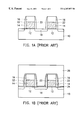
- Self-alignment is a technique in which multiple levels of regions on the wafer are formed using a single mask, thereby eliminating the alignment tolerance required by additional masks. This powerful approach is being used more often as circuit sizes decrease. Self-aligned contacts are often used in memory cells where contacts are limited only by the spacers and field oxide bird's beak or a contact window landing pad. Therefore, the mask contact window can be oversized relative to the contact area underneath, and no contact borders are needed, resulting in significant space saving. Referring to FIGS. 1A-1C, a conventional process of forming a self-aligned contact hole is illustrated in cross-sectional views. The process will be described as follows.
- FIG. 1A shows a semiconductor substrate 10 having two closely spaced field effect transistors with gate electrodes 14 , source/drain diffusion regions 18 , and gate oxides 12 .
- the gate electrodes 14 commonly consisting of polysilicon and silicide, are capped with an insulator 16 of silicon nitride.
- a nitride or oxide layer is formed over the substrate surface using low pressure chemical vapor deposition (LPCVD), which is then anisotropically etched to form sidewall spacers 22 on the sidewalls of the gate electrodes 14 and the cap layers 16 .
- LPCVD low pressure chemical vapor deposition
- a conformal layer of etch barrier material 24 is deposited over the diffusion region 18 , the cap layers 16 , and the sidewall spacers 22 .
- the barrier layer 24 which may also be called the liner layer, typically consists of silicon nitride.
- a layer of insulator 26 is deposited over the substrate as inter-layer dielectric (ILD) and is preferably planarized.
- the insulating layer 26 may consist of one or more dielectric depositions of spin on glass (SOG), silicon oxide, borophosphosilicate (BPSG), and so on.
- a contact hole can be etched in the insulating layer 26 with the liner layer 24 serving as an etch stop, which will be finally removed to expose the diffusion region 18 .
- the etching of the insulating layer 26 is selective to the capping layers 16 and sidewall spacers 22 encapsulating the gate electrodes 14 so that the contact hole is self-aligning in nature.
- the process window can be improved by increasing the etch selectivity
- the highest selectivity of oxide to nitride is only about 30-40 with the current dry etch technology, and the higher the selectivity, the more tapered the contact sidewall profile, as depicted by dotted lines 30 in FIG. 3 C.
- Such a tapered profile causes a significant decrease in the contact area to the substrate, and consequently, increasing the contact resistance.
- the present invention provides a method for forming a self-aligned contact hole, characterized in that the bottom portion of the contact hole is formed by wet etch methods to ensure high selectivity.
- the present method for forming a self-aligned contact includes the steps of: (a) providing a semiconductor substrate having a gate electrode and a diffusion region thereon; (b) forming a conformal layer of etch barrier material overlying the substrate surface including the diffusion region and the upper surface and the sidewalls of the gate electrode; (c) forming an insulating layer overlying the barrier layer; (d) forming a mask layer overlying the insulating layer; (e) etching an opening through the mask layer and part of the way through the insulating layer, aligned with the diffusion region, until the barrier layer is exposed; (f) forming spacers on the sidewalls of the opening; (g) removing the remaining portion of the insulating layer underneath the opening by isotropically etching using the mask layer, the spacers
- the isotropic etch of step (g) can be performed by immersion etching or spraying etching using HF solution or HF vapor as etchant. By using the wet etch methods, a selectivity of higher than 100 for oxide to nitride can be obtained.
- FIGS. 1A through 1C are cross-sectional views illustrating the steps of a conventional method for fabricating a self-aligned contact hole
- FIGS. 2A through 2E are cross-sectional views illustrating the steps for fabricating a self-aligned contact hole according to a preferred embodiment of the invention.
- two closely spaced field effect transistors with gate electrodes 54 , source/drain diffusion regions 58 , and gate oxides 52 are defined in a semiconductor substrate 50 using known processes.
- the gate electrodes 54 preferably consisting of polysilicon and tungsten silicide, are capped with an insulator 56 of silicon nitride.
- the process details for forming such field effect transistors are well known and will not be described here.
- insulating sidewall spacers 52 are formed on the sidewalls of the gate electrodes 64 and the cap layers 56 .
- the sidewall spacers 52 can be formed by depositing a nitride or oxide layer using LPCVD, followed by anisotropically etching back.
- a conformal layer of etch barrier material 64 is deposited over the diffusion region 58 , the cap layers 56 , and the sidewall spacers 62 .
- the barrier layer is typically a silicon nitride layer having a thickness of about 100 to 1000 ⁇ .
- a layer of insulator 66 is deposited over the substrate as inter-layer dielectric (ILD) and is preferably planarized.
- the insulating layer 66 may consist of one or more dielectric depositions of spin on glass (SOG), silicon oxide, borophosphosilicate (BPSG), and so on.
- a mask layer 68 is deposited over the insulating layer 66 .
- the mask layer 68 for example, is a silicon nitride layer with a thickness of about 50 to 500 ⁇ . After this, a photoresist layer 70 with a contact hole pattern aligned with the diffusion region 58 is formed over the mask layer 68 by microlithographic techniques.
- the contact hole pattern is anisotopically etched through the mask layer 68 and part of way through the insulating layer 66 until the barrier layer 64 is exposed.
- an opening 72 in alignment with the diffusion region 58 is formed in the upper portion of the insulating layer. It is preferable that this etch is stopped at the upper most portion of the barrier layer 64 , which can be done by either end point detection or time mode control during the etching process. Note that there are insulator residues 66 a in the opening yet.
- spacers of etch barrier material 74 are formed on the sidewalls of the opening 72 .
- the sidewall spacers 74 can be formed by depositing a conformal silicon nitride layer with a thickness of about 50 to 500 ⁇ over the bottom and sidewalls of opening, followed by anisotropically etching back.
- the insulating layer is thus encapsulated by the mask layer 68 and the sidewall spacers 74 except the portion underneath the opening 72 .
- an isotropic wet etching is performed using the mask layer 68 , the sidewall spacers 74 and the barrier layer 64 as stopping layers, thereby removing any insulator residues left behind in the opening in the previous etching process.
- the mask layer 68 and sidewall spacers 74 serves as etch barriers to protect the insulating layer 66 from being attacked, while the barrier layer 66 protects the diffusion region 58 .
- the isotropic etch can be performed by typical immersion etching or spraying etching using HF solution or HF vapor as etchant. By using these methods, a selectivity of higher than 100 for oxide to nitride can be achieved, much higher than that of dry etch methods (30-40).
- the insulator residues in the contact region can be thoroughly removed even if there is misalignment during the microlithography process.
- full utilization of the contact area is guaranteed, and the process window is significantly improved.
- the conformal barrier layer 64 underneath the opening is anisotropically etched to remove the portion over the diffusion region 58 , thereby completing the contact hole. Simultaneously with this etch, the mask layer 68 overlying the insulating layer 66 is removed. Thereafter, a conductive plug can be formed in the contact hole 72 to electrically connect to the diffusion region 58 .
Abstract
Description
Claims (27)
Applications Claiming Priority (2)
| Application Number | Priority Date | Filing Date | Title |
|---|---|---|---|
| TW88117289 | 1999-10-07 | ||
| TW088117289A TW425668B (en) | 1999-10-07 | 1999-10-07 | Self-aligned contact process |
Publications (1)
| Publication Number | Publication Date |
|---|---|
| US6287957B1 true US6287957B1 (en) | 2001-09-11 |
Family
ID=21642530
Family Applications (1)
| Application Number | Title | Priority Date | Filing Date |
|---|---|---|---|
| US09/468,196 Expired - Lifetime US6287957B1 (en) | 1999-10-07 | 1999-12-21 | Self-aligned contact process |
Country Status (2)
| Country | Link |
|---|---|
| US (1) | US6287957B1 (en) |
| TW (1) | TW425668B (en) |
Cited By (15)
| Publication number | Priority date | Publication date | Assignee | Title |
|---|---|---|---|---|
| US6632741B1 (en) * | 2000-07-19 | 2003-10-14 | International Business Machines Corporation | Self-trimming method on looped patterns |
| US6649503B2 (en) * | 2000-11-30 | 2003-11-18 | Samsung Electronics Co., Ltd. | Methods of fabricating integrated circuit devices having spin on glass (SOG) insulating layers and integrated circuit devices fabricated thereby |
| US20040043542A1 (en) * | 2000-02-03 | 2004-03-04 | Park Jong-Woo | Methods of forming self-aligned contact structures in semiconductor integrated circuit devices |
| US20040127052A1 (en) * | 2002-12-26 | 2004-07-01 | Sung-Kwon Lee | Method for fabricating semiconductor device |
| US20040224454A1 (en) * | 2001-09-11 | 2004-11-11 | Jin Beom-Jun | Methods of manufacturing integrated circuit devices having contact holes using multiple insulating layers |
| US20050085072A1 (en) * | 2003-10-20 | 2005-04-21 | Kim Hyun T. | Formation of self-aligned contact plugs |
| US20050101127A1 (en) * | 2003-11-08 | 2005-05-12 | Hwang Jae-Hee | Method of manufacturing semiconductor device that includes forming self-aligned contact pad |
| US20050142830A1 (en) * | 2003-12-24 | 2005-06-30 | Hynix Semiconductor Inc. | Method for forming a contact of a semiconductor device |
| US20060240654A1 (en) * | 2005-04-22 | 2006-10-26 | Macronix International Co., Ltd. | Process of forming a self-aligned contact in a semiconductor device |
| DE102005063258A1 (en) * | 2005-12-30 | 2007-07-12 | Infineon Technologies Ag | Electrical contacts manufacturing method for e.g. dynamic random access memory cell, involves applying spacer layer on upper side wall region of conductors before arranging contacts, where spacer layer separates conductors from contacts |
| US20090224309A1 (en) * | 2008-03-04 | 2009-09-10 | Kabushiki Kaisha Toshiba | Nonvolatile semiconductor storage device and manufacturing method thereof |
| US20100301486A1 (en) * | 2009-05-29 | 2010-12-02 | Kai Frohberg | High-aspect ratio contact element with superior shape in a semiconductor device for improving liner deposition |
| US20180350662A1 (en) * | 2017-05-31 | 2018-12-06 | Taiwan Semiconductor Manufacturing Co., Ltd. | Semiconductor device and method of fabricating the same |
| US11257833B2 (en) * | 2019-02-26 | 2022-02-22 | Winbond Electronics Corp. | Memory device and manufacturing method thereof |
| US11264419B2 (en) * | 2019-12-30 | 2022-03-01 | Omnivision Technologies, Inc. | Image sensor with fully depleted silicon on insulator substrate |
Citations (1)
| Publication number | Priority date | Publication date | Assignee | Title |
|---|---|---|---|---|
| US6146997A (en) * | 1999-05-11 | 2000-11-14 | Mosel Vitelic, Inc. | Method for forming self-aligned contact hole |
-
1999
- 1999-10-07 TW TW088117289A patent/TW425668B/en not_active IP Right Cessation
- 1999-12-21 US US09/468,196 patent/US6287957B1/en not_active Expired - Lifetime
Patent Citations (1)
| Publication number | Priority date | Publication date | Assignee | Title |
|---|---|---|---|---|
| US6146997A (en) * | 1999-05-11 | 2000-11-14 | Mosel Vitelic, Inc. | Method for forming self-aligned contact hole |
Cited By (32)
| Publication number | Priority date | Publication date | Assignee | Title |
|---|---|---|---|---|
| US6881659B2 (en) * | 2000-02-03 | 2005-04-19 | Samsung Electronics Co., Ltd. | Methods of forming self-aligned contact structures in semiconductor integrated circuit devices |
| US20040043542A1 (en) * | 2000-02-03 | 2004-03-04 | Park Jong-Woo | Methods of forming self-aligned contact structures in semiconductor integrated circuit devices |
| US6632741B1 (en) * | 2000-07-19 | 2003-10-14 | International Business Machines Corporation | Self-trimming method on looped patterns |
| US6649503B2 (en) * | 2000-11-30 | 2003-11-18 | Samsung Electronics Co., Ltd. | Methods of fabricating integrated circuit devices having spin on glass (SOG) insulating layers and integrated circuit devices fabricated thereby |
| US6897109B2 (en) * | 2001-09-11 | 2005-05-24 | Samsung Electronics Co., Ltd. | Methods of manufacturing integrated circuit devices having contact holes using multiple insulating layers |
| US20040224454A1 (en) * | 2001-09-11 | 2004-11-11 | Jin Beom-Jun | Methods of manufacturing integrated circuit devices having contact holes using multiple insulating layers |
| US20040127052A1 (en) * | 2002-12-26 | 2004-07-01 | Sung-Kwon Lee | Method for fabricating semiconductor device |
| US7052999B2 (en) * | 2002-12-26 | 2006-05-30 | Hynix Semiconductor Inc. | Method for fabricating semiconductor device |
| US20050085072A1 (en) * | 2003-10-20 | 2005-04-21 | Kim Hyun T. | Formation of self-aligned contact plugs |
| US20060264047A1 (en) * | 2003-10-20 | 2006-11-23 | Kim Hyun T | Formation of self-aligned contact plugs |
| US7279419B2 (en) | 2003-10-20 | 2007-10-09 | Micron Technology, Inc. | Formation of self-aligned contact plugs |
| US20050101127A1 (en) * | 2003-11-08 | 2005-05-12 | Hwang Jae-Hee | Method of manufacturing semiconductor device that includes forming self-aligned contact pad |
| US7253099B2 (en) | 2003-11-08 | 2007-08-07 | Samsung Electronics Co., Ltd. | Method of manufacturing semiconductor device that includes forming self-aligned contact pad |
| US20050142830A1 (en) * | 2003-12-24 | 2005-06-30 | Hynix Semiconductor Inc. | Method for forming a contact of a semiconductor device |
| US20060240654A1 (en) * | 2005-04-22 | 2006-10-26 | Macronix International Co., Ltd. | Process of forming a self-aligned contact in a semiconductor device |
| US7723229B2 (en) * | 2005-04-22 | 2010-05-25 | Macronix International Co., Ltd. | Process of forming a self-aligned contact in a semiconductor device |
| DE102005063258B4 (en) * | 2005-12-30 | 2008-08-21 | Qimonda Ag | Method for producing an electrical contact for an electrical component and an electrical component |
| DE102005063258A1 (en) * | 2005-12-30 | 2007-07-12 | Infineon Technologies Ag | Electrical contacts manufacturing method for e.g. dynamic random access memory cell, involves applying spacer layer on upper side wall region of conductors before arranging contacts, where spacer layer separates conductors from contacts |
| US20090224309A1 (en) * | 2008-03-04 | 2009-09-10 | Kabushiki Kaisha Toshiba | Nonvolatile semiconductor storage device and manufacturing method thereof |
| US8048798B2 (en) * | 2008-03-04 | 2011-11-01 | Kabushiki Kaisha Toshiba | Method for manufacturing a nonvolatile semiconductor storage device where memory cells are arranged three dimensionally |
| US20100301486A1 (en) * | 2009-05-29 | 2010-12-02 | Kai Frohberg | High-aspect ratio contact element with superior shape in a semiconductor device for improving liner deposition |
| DE102009023251A1 (en) * | 2009-05-29 | 2010-12-02 | Globalfoundries Dresden Module One Limited Liability Company & Co. Kg | A method of making a high aspect ratio contact element having a more favorable shape in a semiconductor device to improve the deposition of a coating |
| DE102009023251B4 (en) * | 2009-05-29 | 2011-02-24 | Globalfoundries Dresden Module One Limited Liability Company & Co. Kg | A method of making a high aspect ratio contact element having a more favorable shape in a semiconductor device to improve the deposition of a coating |
| US20180350662A1 (en) * | 2017-05-31 | 2018-12-06 | Taiwan Semiconductor Manufacturing Co., Ltd. | Semiconductor device and method of fabricating the same |
| US10522392B2 (en) * | 2017-05-31 | 2019-12-31 | Taiwan Semiconductor Manufacturing Co., Ltd. | Semiconductor device and method of fabricating the same |
| US11355387B2 (en) | 2017-05-31 | 2022-06-07 | Taiwan Semiconductor Manufacturing Co., Ltd. | Semiconductor device and method of fabricating the same |
| US20220293459A1 (en) * | 2017-05-31 | 2022-09-15 | Taiwan Semiconductor Manufacturing Co., Ltd. | Semiconductor device and method of fabricating the same |
| US11769690B2 (en) | 2017-05-31 | 2023-09-26 | Taiwan Semiconductor Manufacturing Co., Ltd. | Semiconductor device and method of fabricating the same |
| US11257833B2 (en) * | 2019-02-26 | 2022-02-22 | Winbond Electronics Corp. | Memory device and manufacturing method thereof |
| US20220123007A1 (en) * | 2019-02-26 | 2022-04-21 | Winbond Electronics Corp. | Manufacturing method of memory device |
| US11805644B2 (en) * | 2019-02-26 | 2023-10-31 | Winbond Electronics Corp. | Manufacturing method of memory device |
| US11264419B2 (en) * | 2019-12-30 | 2022-03-01 | Omnivision Technologies, Inc. | Image sensor with fully depleted silicon on insulator substrate |
Also Published As
| Publication number | Publication date |
|---|---|
| TW425668B (en) | 2001-03-11 |
Similar Documents
| Publication | Publication Date | Title |
|---|---|---|
| US6498096B2 (en) | Borderless contact to diffusion with respect to gate conductor and methods for fabricating | |
| US6287957B1 (en) | Self-aligned contact process | |
| US6001726A (en) | Method for using a conductive tungsten nitride etch stop layer to form conductive interconnects and tungsten nitride contact structure | |
| JPH07221194A (en) | Integrated circuit and its preparation | |
| US6278189B1 (en) | High density integrated circuits using tapered and self-aligned contacts | |
| US5989987A (en) | Method of forming a self-aligned contact in semiconductor fabrications | |
| US6015741A (en) | Method for forming self-aligned contact window | |
| KR100224720B1 (en) | Method for forming of contact hole in semiconductor device | |
| US20050275109A1 (en) | Semiconductor device and fabricating method thereof | |
| KR100382727B1 (en) | Method for fabricating pad without void using self-aligned contact etch process in semiconductor device | |
| US20040155277A1 (en) | Method for manufacturing a semiconductor device including a PIP capacitor and a MOS transistor | |
| KR100252039B1 (en) | Method for forming a self-aligned contact hole | |
| US5985766A (en) | Semiconductor processing methods of forming a contact opening | |
| US6255168B1 (en) | Method for manufacturing bit line and bit line contact | |
| US6383921B1 (en) | Self aligned silicide contact method of fabrication | |
| US6146997A (en) | Method for forming self-aligned contact hole | |
| US6248636B1 (en) | Method for forming contact holes of semiconductor memory device | |
| US5266835A (en) | Semiconductor structure having a barrier layer disposed within openings of a dielectric layer | |
| US6559044B1 (en) | Method for forming contacts | |
| KR100333539B1 (en) | Micro contact hole formation method of semiconductor device | |
| KR0151047B1 (en) | Bit line manufacturing method for semiconductor device | |
| US20030045091A1 (en) | Method of forming a contact for a semiconductor device | |
| KR100213203B1 (en) | Semiconductor device with contact hole and process for fabricating the same | |
| KR19990026458A (en) | Self Align Contact Method | |
| KR100338605B1 (en) | Method for forming contact hole of semiconductor |
Legal Events
| Date | Code | Title | Description |
|---|---|---|---|
| AS | Assignment |
Owner name: WORLDWIDE SEMICONDUCTOR MANUFACTURING CORPORATION, Free format text: ASSIGNMENT OF ASSIGNORS INTEREST;ASSIGNOR:LINLIU, KUNG;REEL/FRAME:010508/0560 Effective date: 19991206 |
|
| AS | Assignment |
Owner name: TAIWAN SEMICONDUCTOR MANUFACTURING CO., LTD., TAIW Free format text: ASSIGNMENT OF ASSIGNORS INTEREST;ASSIGNOR:WORLDWIDE SEMICONDUCTOR MANUFACTURING CORP.;REEL/FRAME:010958/0881 Effective date: 20000601 |
|
| STCF | Information on status: patent grant |
Free format text: PATENTED CASE |
|
| FEPP | Fee payment procedure |
Free format text: PAYOR NUMBER ASSIGNED (ORIGINAL EVENT CODE: ASPN); ENTITY STATUS OF PATENT OWNER: LARGE ENTITY |
|
| FPAY | Fee payment |
Year of fee payment: 4 |
|
| FPAY | Fee payment |
Year of fee payment: 8 |
|
| FPAY | Fee payment |
Year of fee payment: 12 |