US6252923B1 - In-situ self-powered monitoring of stored spent nuclear fuel - Google Patents
In-situ self-powered monitoring of stored spent nuclear fuel Download PDFInfo
- Publication number
- US6252923B1 US6252923B1 US09/371,720 US37172099A US6252923B1 US 6252923 B1 US6252923 B1 US 6252923B1 US 37172099 A US37172099 A US 37172099A US 6252923 B1 US6252923 B1 US 6252923B1
- Authority
- US
- United States
- Prior art keywords
- neutron
- container
- nuclear fuel
- spent nuclear
- detectors
- Prior art date
- Legal status (The legal status is an assumption and is not a legal conclusion. Google has not performed a legal analysis and makes no representation as to the accuracy of the status listed.)
- Expired - Lifetime
Links
- 239000002915 spent fuel radioactive waste Substances 0.000 title claims abstract description 54
- 238000012544 monitoring process Methods 0.000 title claims description 12
- 238000011065 in-situ storage Methods 0.000 title description 2
- 239000004065 semiconductor Substances 0.000 claims abstract description 57
- 230000005251 gamma ray Effects 0.000 claims abstract description 40
- 230000004907 flux Effects 0.000 claims abstract description 29
- 239000000463 material Substances 0.000 claims description 23
- 230000000712 assembly Effects 0.000 claims description 16
- 238000000429 assembly Methods 0.000 claims description 16
- 239000011358 absorbing material Substances 0.000 claims description 9
- 230000004323 axial length Effects 0.000 claims description 7
- 229910003460 diamond Inorganic materials 0.000 claims description 4
- 239000010432 diamond Substances 0.000 claims description 4
- 229910001218 Gallium arsenide Inorganic materials 0.000 claims description 3
- 229910052732 germanium Inorganic materials 0.000 claims description 3
- 229910052710 silicon Inorganic materials 0.000 claims description 3
- 229910004613 CdTe Inorganic materials 0.000 claims description 2
- 229910052980 cadmium sulfide Inorganic materials 0.000 claims description 2
- 238000003466 welding Methods 0.000 claims description 2
- 229910004611 CdZnTe Inorganic materials 0.000 claims 1
- ZASWJUOMEGBQCQ-UHFFFAOYSA-L dibromolead Chemical compound Br[Pb]Br ZASWJUOMEGBQCQ-UHFFFAOYSA-L 0.000 claims 1
- HTUMBQDCCIXGCV-UHFFFAOYSA-N lead oxide Chemical compound [O-2].[Pb+2] HTUMBQDCCIXGCV-UHFFFAOYSA-N 0.000 claims 1
- RQQRAHKHDFPBMC-UHFFFAOYSA-L lead(ii) iodide Chemical compound I[Pb]I RQQRAHKHDFPBMC-UHFFFAOYSA-L 0.000 claims 1
- 230000005855 radiation Effects 0.000 abstract description 16
- 238000003860 storage Methods 0.000 abstract description 11
- 238000005259 measurement Methods 0.000 abstract description 9
- 231100001261 hazardous Toxicity 0.000 abstract 1
- 239000002245 particle Substances 0.000 description 31
- 229910010271 silicon carbide Inorganic materials 0.000 description 19
- HBMJWWWQQXIZIP-UHFFFAOYSA-N silicon carbide Chemical compound [Si+]#[C-] HBMJWWWQQXIZIP-UHFFFAOYSA-N 0.000 description 19
- 238000006073 displacement reaction Methods 0.000 description 16
- 239000000446 fuel Substances 0.000 description 15
- 150000002500 ions Chemical class 0.000 description 14
- 239000000758 substrate Substances 0.000 description 10
- XLYOFNOQVPJJNP-UHFFFAOYSA-N water Substances O XLYOFNOQVPJJNP-UHFFFAOYSA-N 0.000 description 10
- 239000007795 chemical reaction product Substances 0.000 description 9
- 238000000034 method Methods 0.000 description 9
- IJGRMHOSHXDMSA-UHFFFAOYSA-N Atomic nitrogen Chemical compound N#N IJGRMHOSHXDMSA-UHFFFAOYSA-N 0.000 description 6
- VYPSYNLAJGMNEJ-UHFFFAOYSA-N Silicium dioxide Chemical compound O=[Si]=O VYPSYNLAJGMNEJ-UHFFFAOYSA-N 0.000 description 6
- 239000011810 insulating material Substances 0.000 description 6
- 230000005284 excitation Effects 0.000 description 5
- 230000004992 fission Effects 0.000 description 5
- 229910052734 helium Inorganic materials 0.000 description 5
- 230000001965 increasing effect Effects 0.000 description 5
- 229910052751 metal Inorganic materials 0.000 description 5
- 239000002184 metal Substances 0.000 description 5
- PXHVJJICTQNCMI-UHFFFAOYSA-N nickel Substances [Ni] PXHVJJICTQNCMI-UHFFFAOYSA-N 0.000 description 5
- XEEYBQQBJWHFJM-UHFFFAOYSA-N Iron Chemical compound [Fe] XEEYBQQBJWHFJM-UHFFFAOYSA-N 0.000 description 4
- 230000015556 catabolic process Effects 0.000 description 4
- 238000006731 degradation reaction Methods 0.000 description 4
- 238000001514 detection method Methods 0.000 description 4
- 239000001307 helium Substances 0.000 description 4
- SWQJXJOGLNCZEY-UHFFFAOYSA-N helium atom Chemical compound [He] SWQJXJOGLNCZEY-UHFFFAOYSA-N 0.000 description 4
- 229910052744 lithium Inorganic materials 0.000 description 4
- 238000004519 manufacturing process Methods 0.000 description 4
- 229910003465 moissanite Inorganic materials 0.000 description 4
- 230000035515 penetration Effects 0.000 description 4
- WHXSMMKQMYFTQS-UHFFFAOYSA-N Lithium Chemical compound [Li] WHXSMMKQMYFTQS-UHFFFAOYSA-N 0.000 description 3
- 229910000831 Steel Inorganic materials 0.000 description 3
- 239000003570 air Substances 0.000 description 3
- XAGFODPZIPBFFR-UHFFFAOYSA-N aluminium Chemical compound [Al] XAGFODPZIPBFFR-UHFFFAOYSA-N 0.000 description 3
- 230000005540 biological transmission Effects 0.000 description 3
- 229910052796 boron Inorganic materials 0.000 description 3
- 238000006243 chemical reaction Methods 0.000 description 3
- 238000005229 chemical vapour deposition Methods 0.000 description 3
- 229910052681 coesite Inorganic materials 0.000 description 3
- 229910052906 cristobalite Inorganic materials 0.000 description 3
- 230000003247 decreasing effect Effects 0.000 description 3
- 238000013461 design Methods 0.000 description 3
- 229910001416 lithium ion Inorganic materials 0.000 description 3
- 229910052759 nickel Inorganic materials 0.000 description 3
- 229910052757 nitrogen Inorganic materials 0.000 description 3
- 230000010355 oscillation Effects 0.000 description 3
- 230000021715 photosynthesis, light harvesting Effects 0.000 description 3
- BASFCYQUMIYNBI-UHFFFAOYSA-N platinum Substances [Pt] BASFCYQUMIYNBI-UHFFFAOYSA-N 0.000 description 3
- 239000000523 sample Substances 0.000 description 3
- 238000007789 sealing Methods 0.000 description 3
- 239000000377 silicon dioxide Substances 0.000 description 3
- 239000007787 solid Substances 0.000 description 3
- 229910001220 stainless steel Inorganic materials 0.000 description 3
- 239000010935 stainless steel Substances 0.000 description 3
- 239000010959 steel Substances 0.000 description 3
- 229910052682 stishovite Inorganic materials 0.000 description 3
- 229910052905 tridymite Inorganic materials 0.000 description 3
- 238000009423 ventilation Methods 0.000 description 3
- ZOXJGFHDIHLPTG-UHFFFAOYSA-N Boron Chemical compound [B] ZOXJGFHDIHLPTG-UHFFFAOYSA-N 0.000 description 2
- RYGMFSIKBFXOCR-UHFFFAOYSA-N Copper Chemical compound [Cu] RYGMFSIKBFXOCR-UHFFFAOYSA-N 0.000 description 2
- CPLXHLVBOLITMK-UHFFFAOYSA-N Magnesium oxide Chemical compound [Mg]=O CPLXHLVBOLITMK-UHFFFAOYSA-N 0.000 description 2
- 229910052581 Si3N4 Inorganic materials 0.000 description 2
- XUIMIQQOPSSXEZ-UHFFFAOYSA-N Silicon Chemical compound [Si] XUIMIQQOPSSXEZ-UHFFFAOYSA-N 0.000 description 2
- 239000006096 absorbing agent Substances 0.000 description 2
- 239000000853 adhesive Substances 0.000 description 2
- 230000001070 adhesive effect Effects 0.000 description 2
- 230000004075 alteration Effects 0.000 description 2
- 229910052782 aluminium Inorganic materials 0.000 description 2
- 230000008901 benefit Effects 0.000 description 2
- 238000009835 boiling Methods 0.000 description 2
- 230000008859 change Effects 0.000 description 2
- 239000004020 conductor Substances 0.000 description 2
- 229910052802 copper Inorganic materials 0.000 description 2
- 239000010949 copper Substances 0.000 description 2
- 238000000151 deposition Methods 0.000 description 2
- 230000008021 deposition Effects 0.000 description 2
- 230000006866 deterioration Effects 0.000 description 2
- 238000009826 distribution Methods 0.000 description 2
- 229910052737 gold Inorganic materials 0.000 description 2
- 239000010931 gold Substances 0.000 description 2
- 239000012535 impurity Substances 0.000 description 2
- 229910052742 iron Inorganic materials 0.000 description 2
- 229910052697 platinum Inorganic materials 0.000 description 2
- 239000002574 poison Substances 0.000 description 2
- 231100000614 poison Toxicity 0.000 description 2
- 230000008569 process Effects 0.000 description 2
- 239000000047 product Substances 0.000 description 2
- HQVNEWCFYHHQES-UHFFFAOYSA-N silicon nitride Chemical compound N12[Si]34N5[Si]62N3[Si]51N64 HQVNEWCFYHHQES-UHFFFAOYSA-N 0.000 description 2
- OORLZFUTLGXMEF-UHFFFAOYSA-N sulfentrazone Chemical compound O=C1N(C(F)F)C(C)=NN1C1=CC(NS(C)(=O)=O)=C(Cl)C=C1Cl OORLZFUTLGXMEF-UHFFFAOYSA-N 0.000 description 2
- 206010073306 Exposure to radiation Diseases 0.000 description 1
- 229910002601 GaN Inorganic materials 0.000 description 1
- 229910005540 GaP Inorganic materials 0.000 description 1
- JMASRVWKEDWRBT-UHFFFAOYSA-N Gallium nitride Chemical compound [Ga]#N JMASRVWKEDWRBT-UHFFFAOYSA-N 0.000 description 1
- UFHFLCQGNIYNRP-UHFFFAOYSA-N Hydrogen Chemical compound [H][H] UFHFLCQGNIYNRP-UHFFFAOYSA-N 0.000 description 1
- RTAQQCXQSZGOHL-UHFFFAOYSA-N Titanium Chemical compound [Ti] RTAQQCXQSZGOHL-UHFFFAOYSA-N 0.000 description 1
- YZCKVEUIGOORGS-NJFSPNSNSA-N Tritium Chemical compound [3H] YZCKVEUIGOORGS-NJFSPNSNSA-N 0.000 description 1
- 229910052770 Uranium Inorganic materials 0.000 description 1
- 238000009825 accumulation Methods 0.000 description 1
- 230000006978 adaptation Effects 0.000 description 1
- 238000007792 addition Methods 0.000 description 1
- 238000013459 approach Methods 0.000 description 1
- 238000003491 array Methods 0.000 description 1
- NWAIGJYBQQYSPW-UHFFFAOYSA-N azanylidyneindigane Chemical compound [In]#N NWAIGJYBQQYSPW-UHFFFAOYSA-N 0.000 description 1
- 238000009529 body temperature measurement Methods 0.000 description 1
- 238000004364 calculation method Methods 0.000 description 1
- 239000000919 ceramic Substances 0.000 description 1
- 239000011248 coating agent Substances 0.000 description 1
- 238000000576 coating method Methods 0.000 description 1
- 238000012790 confirmation Methods 0.000 description 1
- 239000013078 crystal Substances 0.000 description 1
- 238000013480 data collection Methods 0.000 description 1
- 230000007812 deficiency Effects 0.000 description 1
- 239000002019 doping agent Substances 0.000 description 1
- 238000004980 dosimetry Methods 0.000 description 1
- 239000012634 fragment Substances 0.000 description 1
- 239000007789 gas Substances 0.000 description 1
- GNPVGFCGXDBREM-UHFFFAOYSA-N germanium atom Chemical compound [Ge] GNPVGFCGXDBREM-UHFFFAOYSA-N 0.000 description 1
- PCHJSUWPFVWCPO-UHFFFAOYSA-N gold Chemical compound [Au] PCHJSUWPFVWCPO-UHFFFAOYSA-N 0.000 description 1
- 239000001257 hydrogen Substances 0.000 description 1
- 229910052739 hydrogen Inorganic materials 0.000 description 1
- 238000012625 in-situ measurement Methods 0.000 description 1
- 230000001939 inductive effect Effects 0.000 description 1
- YEXPOXQUZXUXJW-UHFFFAOYSA-N lead(II) oxide Inorganic materials [Pb]=O YEXPOXQUZXUXJW-UHFFFAOYSA-N 0.000 description 1
- 239000000395 magnesium oxide Substances 0.000 description 1
- 230000007246 mechanism Effects 0.000 description 1
- 239000000203 mixture Substances 0.000 description 1
- 238000012986 modification Methods 0.000 description 1
- 230000004048 modification Effects 0.000 description 1
- 150000004767 nitrides Chemical class 0.000 description 1
- 239000003758 nuclear fuel Substances 0.000 description 1
- 238000004806 packaging method and process Methods 0.000 description 1
- 230000000737 periodic effect Effects 0.000 description 1
- 230000035699 permeability Effects 0.000 description 1
- 230000002285 radioactive effect Effects 0.000 description 1
- 239000012857 radioactive material Substances 0.000 description 1
- 239000010703 silicon Substances 0.000 description 1
- 238000000638 solvent extraction Methods 0.000 description 1
- 239000000126 substance Substances 0.000 description 1
- 238000004347 surface barrier Methods 0.000 description 1
- 239000010409 thin film Substances 0.000 description 1
- 239000010936 titanium Substances 0.000 description 1
- 229910052719 titanium Inorganic materials 0.000 description 1
- 229910052722 tritium Inorganic materials 0.000 description 1
- JFALSRSLKYAFGM-UHFFFAOYSA-N uranium(0) Chemical compound [U] JFALSRSLKYAFGM-UHFFFAOYSA-N 0.000 description 1
Images


Classifications
-
- G—PHYSICS
- G21—NUCLEAR PHYSICS; NUCLEAR ENGINEERING
- G21C—NUCLEAR REACTORS
- G21C17/00—Monitoring; Testing ; Maintaining
- G21C17/06—Devices or arrangements for monitoring or testing fuel or fuel elements outside the reactor core, e.g. for burn-up, for contamination
-
- G—PHYSICS
- G21—NUCLEAR PHYSICS; NUCLEAR ENGINEERING
- G21F—PROTECTION AGAINST X-RADIATION, GAMMA RADIATION, CORPUSCULAR RADIATION OR PARTICLE BOMBARDMENT; TREATING RADIOACTIVELY CONTAMINATED MATERIAL; DECONTAMINATION ARRANGEMENTS THEREFOR
- G21F5/00—Transportable or portable shielded containers
- G21F5/06—Details of, or accessories to, the containers
-
- Y—GENERAL TAGGING OF NEW TECHNOLOGICAL DEVELOPMENTS; GENERAL TAGGING OF CROSS-SECTIONAL TECHNOLOGIES SPANNING OVER SEVERAL SECTIONS OF THE IPC; TECHNICAL SUBJECTS COVERED BY FORMER USPC CROSS-REFERENCE ART COLLECTIONS [XRACs] AND DIGESTS
- Y02—TECHNOLOGIES OR APPLICATIONS FOR MITIGATION OR ADAPTATION AGAINST CLIMATE CHANGE
- Y02E—REDUCTION OF GREENHOUSE GAS [GHG] EMISSIONS, RELATED TO ENERGY GENERATION, TRANSMISSION OR DISTRIBUTION
- Y02E30/00—Energy generation of nuclear origin
- Y02E30/30—Nuclear fission reactors
Definitions
- the present invention relates to monitoring of spent nuclear fuel, and more particularly relates to in-situ, self-powered monitoring of spent nuclear fuel stored in containers.
- the container or canister, and its associated surrounding cask must meet several criteria.
- the container must provide containment integrity to prevent the release of radioactive material during normal or hypothetical accident conditions, as well as structural integrity in supporting the weight load of the contained fuel.
- Thermal protection is required to provide adequate dissipation of the decay heat produced by the spent nuclear fuel, to avoid compromising the integrity of the fuel or the materials of the container or cask.
- Adequate radiation shielding must also be provided to limit the radiation field external to the package to acceptable values.
- the container must also protect against the possibility of nuclear criticality, since the contained fuel could represent a critical mass if the system's engineered features were removed or sufficiently degraded, or if the fuel geometry were radically altered through structural degradation.
- the containers are sealed upon loading, often by double welding, so that re-entry to perform measurements is often not an acceptable option. Instrumentation penetrations are generally regarded as unacceptable because of increased risk of confinement system failure. Because of the uniformity in the manufacture of such systems, monitoring may be performed on a statistically acceptable subset of containers for a given fuel type, to ensure safety of the entire population of containers.
- the present invention has been developed in view of the foregoing, and to overcome other deficiencies of the prior art.
- the present invention provides a method and apparatus which allow remote monitoring of stored spent nuclear fuel, without breeching the containment boundary of the containers in which the spent nuclear fuel is stored.
- Detectors can be configured as an integral part of a spent fuel container, or as a measurement probe which can be placed adjacent the spent fuel container while it is contained within a storage cask.
- Monitoring of the neutron and ⁇ -ray fields could be used to indicate the integrity of the fuel or neutron absorber, and the presence of water in the container.
- Temperature measurements may also be made to determine the temperature profile in the container. Structural degradation or failure of key components within the container may also be detected.
- An object of the present invention is to provide a system for measuring neutron and ⁇ -ray flux emitted from spent nuclear fuel including a container, spent nuclear fuel in the container, and at least one detector positioned to receive the neutron and ⁇ -ray flux from the spent nuclear fuel.
- Multiple such “neutron and ⁇ -ray” detectors are preferably positioned in an array either inside or outside the container.
- the neutron and ⁇ -ray detectors preferably include a semiconductor active region comprising silicon carbide or metal.
- a cask made of concrete or metal may be placed around the container and detectors to provide shielding, support, and impact protection.
- Another object of the present invention is to provide a method of measuring neutron and ⁇ -ray flux from spent nuclear fuel, the method comprising the steps of placing spent nuclear fuel in a container, sealing the container, and measuring neutron and ⁇ -ray flux from the spent nuclear fuel with at least one neutron and ⁇ -ray detector.
- the detector may be sealed inside the container or positioned on the exterior of the container.
- Another object of the present invention is to provide a method and apparatus for measuring the temperature of spent nuclear fuel in a container.
- Another object of the present invention is to provide a method and apparatus for sensing the structural integrity of key components of containers for spent nuclear fuel.
- FIG. 1 is a side perspective view of spent nuclear fuel assemblies positioned inside a container, including an array of detectors for simultaneously measuring neutron and ⁇ -ray flux in accordance with the present invention.
- FIG. 2 is a top view of the spent nuclear fuel assemblies and container of FIG. 1 .
- FIG. 3 is a side sectional view of a spent nuclear fuel container positioned inside a typical storage cask, including one embodiment of an array of neutron and ⁇ -ray detectors in accordance with the present invention.
- FIG. 4 is a partially schematic side sectional view of a semiconductor neutron detector in accordance with an embodiment of the present invention.
- FIG. 5 is a partially schematic side sectional view of a semiconductor neutron detector in accordance with another embodiment of the present invention.
- FIGS. 6-9 are graphs of detector depth versus ionization and vacancy production representing energy dissipation curves for various silicon carbide neutron detectors of the present invention.
- FIGS. 10 and 11 are partially schematic side sectional views of a sensor for structural integrity of selected joints or components in accordance with another embodiment of the present invention.
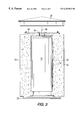
- FIG. 1 is an isometric view and FIG. 2 is a top view of a spent nuclear fuel container 10 having multiple spent nuclear fuel assemblies 12 stored therein.
- the fuel assemblies 12 extend substantially the entire axial length of the container 10 .
- a neutron absorbing material 14 such as boral neutron poison or borated stainless steel, is located around the spent nuclear fuel assemblies 12 within the container 10 .
- the container 10 may be of any desired size and, for example, typically has a length of about 190 inches and an outer diameter of about 66 inches, with a capacity for twenty-one to twenty-four pressurized water reactor spent nuclear fuel assemblies of forty-four to seventy-four boiling water reactor spent nuclear fuel assemblies 12 .
- the spent fuel assemblies 12 may be from a pressurized water reactor (PWR) or a boiling water reactor (BWR).
- a circular lid (not shown) is typically double welded or otherwise multiply sealed to the top of the container 10 in a known manner to seal the container after the spent fuel assemblies have been loaded.
- an array of detectors 30 is placed adjacent the container 10 .
- the detectors 30 are used to simultaneously measure neutron and ⁇ -ray flux, as more fully described below.
- temperature sensors may be used in addition to the neutron and ⁇ -ray detectors 30 to measure a temperature profile of the container 10 .
- the neutron detectors 30 may be mounted on a strip 16 or other suitable support structure that allows placement of the detectors 30 adjacent or within the canister 10 in the desired locations.
- the strip 16 includes wires or other suitable electrical conductors for transmitting signals generated by the neutron detectors 30 .
- a wire 18 or other suitable conductor transmits the signals from the strip 16 .
- the strip 16 preferably comprises a flexible material such as an insulating plastic resistant to high temperatures and radiation, which facilitates placement of the arrays 30 adjacent the container 10 .
- the neutron and ⁇ -ray detectors and the (optional) thermal sensors might alternatively be located inside the container.
- the sealed spent nuclear fuel container 10 may be stored inside a concrete cask 20 having a base 22 and lid 24 .
- the base 22 and lid 24 surround and contain the cask 20 according to the specific manufacturer's design.
- a ventilation opening 26 is provided in the lid 24 .
- a cover assembly 28 is placed over the lid 24 and rests on the cask 20 .
- the area between the inner wall of the cask 20 and outer wall of the container 10 defines an annular region in which the neutrons and ⁇ -ray detectors 30 are positioned.
- a thin steel annular heat shield may be used between the canister and cask.
- the neutron and ⁇ -ray detectors 30 are held in the desired location in relation to the container 10 by the strip 16 .
- the wire 18 extends through the ventilation opening or another suitable penetration 26 to the exterior of the cask 20 in order to transmit the signals generated by the neutron and ⁇ -ray detectors 30 .
- the neutron and ⁇ -ray detectors 30 are used to monitor the flux of energetic neutrons and ⁇ -ray emitted by the spent nuclear fuel assemblies 12 .
- the detector array may be periodically interrogated, such as once every few months. By performing this interrogation when the spent nuclear fuel container 10 is put into storage, a baseline profile of neutron flux and ⁇ -ray flux versus container height is established. Subsequent variations from this profile can be used to determine several parameters of interest.
- neutron absorbing materials 14 e.g., boral neutron poison, which typically extends within the container 10 over the entire length of the fuel assemblies 12 , might decompose over a period of decades as a result of corrosive processes. If the geometry of the neutron absorbing material 14 were to alter, for example, by dropping to a lower height, the neutron profile would reflect this circumstance. In the region of height from which the neutron absorber 14 has been removed, the detectors 30 would report locally higher neutron flux and ⁇ -ray flux, due to locally greater neutron multiplication, due to fission and the overall neutron flux would rise somewhat due to neutron leakage from this region.
- water incursion into the container 10 would produce a region of locally greater neutron flux and ⁇ -ray flux due to an increase in the fission reaction rate at the bottom of the spent fuel assembly region, which would lead to a skewing of the neutron and ⁇ -ray flux profiles toward the bottom and a slight overall increase in neutron flux due to neutron leakage from the bottom region.
- confirmation may be obtained by deploying a passive gamma spectrometer which would record the presence of the 2223 keV prompt gamma ray produced by the capture of thermal neutrons in hydrogen.
- This measurement would preferably be made in a configuration which isolates the spectrometer from 2223 keV gamma rays generated in other hydrogenous material, or in which there is sufficiently little other hydrogenous material that a foreground-background measurement approach can be taken.
- Alteration of the neutron absorbing material 14 or incursion of water into the container 10 may thus be detected in a timely fashion in accordance with the present invention. This allows the timely monitoring of other containers to determine the need for any possible fuel reloading.
- the monitoring of the fuel neutron field can be achieved by providing small wells in the inner wall of the surrounding cask, into which are placed passive, interrogable monitors such as a conventional Solid State Track Recorder (SSTR) neutron dosimeter.
- passive, interrogable monitors such as a conventional Solid State Track Recorder (SSTR) neutron dosimeter.
- SSTR Solid State Track Recorder
- a string of such sensors can be deployed from the cask opening beneath the rain cover or other suitable penetation, using a flexible holder which can be fastened to the steel container outer wall or other suitable surface. Proper placement can be assured by aligning the holder with fiduciary marks. In this way, the neutron field sensors could be retrieved for readout and replaced as desired.
- the array of neutron and ⁇ -ray detectors 30 comprises a set of semiconductor detectors which have been specially configured to be both neutron and ⁇ -ray -sensitive.
- Such an array may be configured to provide a low volume probe suitable for deployment within the region between the container outer radius and the inner radius of a concrete storage cask, as shown in FIG. 3 .
- the sensor strip 16 can be deployed by various means such as passing the strip through the ventilation opening 26 or other suitable penetration into the annular space between the container 10 and cask 20 . Similar deployment is possible for storage in a horizontal orientation.
- the preferred semiconductor neutron and ⁇ -ray detectors 30 are radiation hard, can function in high temperature environments and could be configured to function without application of an external bias voltage, they may be loaded into the container 10 prior to sealing, without requiring external electrical connections.
- the detector 30 By using the detector 30 as a variable current source component of a low-frequency LRC circuit, the signal may be detected remotely using a pickup loop having a frequency varied to match the LRC output.
- the signal may then be picked up remotely using a pickup coil whose frequency is scanned to match the oscillation frequency. For frequencies less than or on the order of about 20 Hz, satisfactory transmission of the signal through a container wall of roughly one inch thickness of Type 304 or a similar stainless steel may be achieved. At 20° C. the resistivity of copper is about 1.7 ⁇ -cm and that of iron is about 9.7 ⁇ -cm. Copper exhibits a skin depth for attenuation of electromagnetic signals of 0.85 cm for a signal of 60 Hz frequency. The skin depth (representing attenuation of an incident signal by the factor 1/e) varies according to the formula:
- iron is expected to exhibit a skin depth of about 2.1 cm (0.8 inch), while at 20 Hz this depth would be of the order of about 3.6 cm (1.4 inch).
- the skin depth in stainless steel for a 20 Hz signal is on the order of one inch or greater, and satisfactory transmission through the container wall can be achieved.
- the circuit may be coupled to a generator of acoustic signals in the Mhz frequency range to achieve satisfactory signal penetration through the container wall.
- the attenuation of a 2 Mhz acoustic signal in worked steel is less than 10 dB/meter. For a thickness of one inch, only a few percent of the intensity of a 2 Mhz acoustic signal would be expected to be lost during transmission, which is satisfactory.
- thermoelectric generating device within the container which utilizes a small portion of the thermal heat output from the fuel.
- 10-year cooled PWR fuel of typical burnup of 40,000 MWD/MTU has a heat output of roughly one kilowatt per assembly, whereas thermoelectric generators with a 50 watt heat source can produce 3 watts of electric power.
- neutron and ⁇ -ray field sensing may be achieved either through the application of passive or active sensors external to the surface of the container 10 , or through the placement of sensors within the container.
- the preferred semiconductor neutron and ⁇ -ray detectors 30 of the present invention preferably comprise a neutron converter layer and a semiconductor active region which is designed to avoid radiation damage to the semiconductor material.
- Deterioration of prior art solid state radiation detectors caused by damage by energetic particles is a well known phenomenon.
- the accumulation of radiation damage in the semiconductor material leads to increased leakage current and decreased charge collection efficiency.
- This radiation damage is caused by the displacement of atoms in the semiconductor by the energetic charged particles. Over time, this damage causes substantial deterioration of detector performance.
- the neutron detector of the present invention takes advantage of the change in the partitioning between electronic excitation and displacement events along the range of the charged particle. For high energy alpha particles ( 4 He ions), electron excitation is the predominant energy loss mechanism. As the particle loses energy, the importance of displacement damage increases. Most of the displacement damage therefore occurs near the end of the range of travel of the charged particles.
- the type of neutron converter layer, the type of semiconductor material, and the thickness and placement of the semiconductor active region are preferably controlled to allow the charged particles to pass through the active semiconductor region without substantial displacement damage.
- the semiconductor active region is sufficiently thin to avoid displacement damage, but is thick enough to allow sufficient ionization or electron excitation to create a measurable electronic pulse.
- the relatively thin semiconductor detector is substantially less susceptible to radiation damage than conventional detectors.
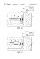
- FIG. 4 schematically illustrates a neutron detector which may be used individually or in an array in accordance with the present invention.
- the neutron detector 30 preferably includes a substrate 32 made of a semiconductor material such as SiC, GaAs, CdTe, diamond, Ge, Si or other appropriate material.
- the substrate 32 preferably has a thickness of about 100 to 1000 microns.
- the substrate 32 is preferably made of temperature resistant materials such as SiC, diamond, silicon nitride, gallium nitride and indium nitride. Where SiC is used as the substrate 32 it may be doped with sufficient amounts of nitrogen or other appropriate impurities to provide sufficient conductivity.
- the substrate 32 may be formed by processes such as high-purity crystal growth or chemical vapor deposition.
- a semiconductor P-N junction is formed by an N-type semiconductor layer 34 and a P-type semiconductor layer 36 .
- the N-type and P-type semiconductor layers 34 and 36 define the semiconductor active region of the neutron detector 30 .
- Silicon and germanium are suitable semiconductor materials.
- the semiconductor active region 34 , 36 is preferably made of materials capable of operating at elevated temperatures, such as SiC, diamond, GaAs, GaP, PbO and CdS.
- SiC is used as the N-type and P-type layers
- such layers are preferably formed by chemical vapor deposition of layers containing an appropriate amount of impurity atoms to increase conductivity.
- typical concentrations in the N- and P-type layers are about 10 15 and greater than about 10 19 atoms per cm 3 , respectively.
- While the active region shown in FIG. 4 comprises a P-N junction, other types of solid state active regions may be used such as Schottky diodes, diffused junction devices, ion implanted diodes or surface barrier detectors.
- a Schottky diode may be placed adjacent to a neutron converter layer comprising boron, lithium, uranium or other suitable material.
- the neutron converter material may optionally serve as the metal rectifying Schottky contact.
- a Schottky diode may be used comprising a contact metal layer of Au, Ni or Pt, an n ⁇ layer of SiC, an n+ layer of SiC, and a conductive SiC substrate.
- electrical contacts are made to the semiconductor active region 34 , 36 by means of the conductive substrate 32 and a thin conductive contact 38 .
- Conventional electrical connections may be made to the substrate 32 and the contact 38 to receive electronic signals from the semiconductor active region 34 , 36 during operation of the detector.
- the contact 38 preferably has a thickness of from about 0.075 to 1 micron, and is made of any suitable material such as gold, platinum, aluminum, titanium or nickel.
- An optional insulating material 40 may be provided around at least a portion of the semiconductor active region 34 , 36 in order to protect the active region from mechanical stresses and/or chemical attack.
- the insulating material 40 may also be used to space the semiconductor active region 34 , 36 a desired distance from a neutron converter layer 42 , as more fully described below.
- the insulating material 40 may comprise any suitable material such as oxides, nitrides and phosphides. For high temperature operations, oxides such as SiO 2 are particularly suitable.
- the SiO 2 layer may be formed by methods such as chemical vapor deposition.
- the semiconductor detector 30 includes a neutron converter layer 42 which generates charged particles when the layer is impinged by neutrons.
- the neutron converter layer may comprise a relatively thin film or coating, or may comprise a doped region of the device.
- the composition of the neutron converter layer 42 is selected such that upon impingement by neutrons, charged particles such as 1 H, 3 H, 7 Li and 4 He ions are generated. Species capable of generating such charged particles include 6 Li, 10 B, H, and 3 He.
- fissionable materials such as 235 U, 233 U or 239 PU can be used to produced charged particles in the form of energetic fission fragments.
- the size of the semiconductor active region 34 , 36 and its placement in relation to the neutron converter layer 42 are preferably controlled in order to minimize radiation damage.
- the neutron converter layer 42 is relatively thin, having a thickness A preferably ranging from about 0.1 to about 10 microns.
- the optional insulating material 40 has a thickness B which is selected in order to minimize displacement damage caused by charged particles, as more fully described below.
- the thickness B of the insulating material 40 typically ranges from 0 to 10 microns or more.
- the P-type semiconductor layer 36 has a thickness C, while the N-type semiconductor layer 34 has a thickness D.
- the thickness C preferably ranges from about 0.1 to about 5 microns, while the thickness D preferably ranges from about 1 to about 10 microns.
- the semiconductor active region which is defined by the N-type and P-type layers 34 and 36 , has a thickness E.
- the thickness E preferably ranges from about 1 to about 15 microns, and is selected such that dislocation damage caused by charged particles
- the neutron converter layer 42 upon impingement by neutrons, some charged particles exit the neutron converter layer 42 in a normal direction N. As more fully described below, a charged particle traveling along direction N will cause electron excitation events as it travels, and will eventually come to rest a distance R N from the neutron converter layer 42 .
- the semiconductor active region 34 , 36 having the thickness E is positioned in relation to the neutron converter layer 42 such that the charged particles traveling in the direction N cause ionization within the thickness of the semiconductor active region E, and pass through the active region before they come to rest. In this manner, dislocation damage within the active region is minimized.
- charged particles exiting the neutron converter layer 42 will also travel at non-normal angles, such as in the oblique direction O.
- Charged particles traveling along direction O pass through the semiconductor active region 34 , 36 and come to rest a distance R o from the neutron converter layer 42 .
- the charged particles thus pass through the semiconductor active region 34 , 36 in many different directions ranging from normal angles N to relatively shallow oblique angles O.
- the range of the charged particles is defined by a band R which is located away from the neutron converter layer a minimum distance of R o and a maximum distance of R N .
- the range of the charged particles falls in a band R outside of the semiconductor active region 34 , 36 . Instead of causing dislocation damage within the active region, the charged particles come to rest in the substrate 32 .
- FIG. 5 schematically illustrates a semiconductor detector 30 suitable for use in accordance with another embodiment of the present invention.
- the detector 30 of FIG. 5 likewise includes a substrate 32 having an N-type semiconductor layer 34 and P-type semiconductor layer 36 disposed thereon.
- An electrical contact 38 and optional insulating material 40 are also incorporated in the detector of FIG. 5.
- a collimator 44 is positioned between the active region 34 , 36 and the neutron converter layer 42 .
- the collimator 44 may be made of any suitable ion absorbing material such as SiO 2 , SiC or silicon nitride.
- the collimator 44 includes an inner passage 48 having a length F and a width G.
- the inner passage may comprise a gas such as air, nitrogen or helium.
- a cap 46 made of any suitable material such as aluminum or nickel provides support for the neutron converter layer 42 .
- the collimator 44 is used to reduce the number of charged particles which enter the semiconductor active region 34 , 36 at shallow angles.
- the height F of the inner passage 48 is preferably at least twice the width G of the passage. Charged particles exiting the neutron converter layer 42 at highly oblique angles are absorbed by the walls of the collimator 44 and do not pass into the active region 34 , 36 .
- charged particles traveling in a normal direction N come to rest a distance R N from the neutron converter layer 42 .
- Charged particles traveling in an oblique direction O come to rest a distance R o away from the neutron converter layer 42 .
- the range of the charged particles is defined by a band R which is located a minimum distance R o from the neutron converter layer 42 and a maximum distance R N from the neutron converter layer.
- Energy deposition curves for charged particles in the detector material may be used to determine the appropriate thickness of the semiconductor active region. Such energy deposition curves may be established from the TRIM computer code developed by Biersack and Ziegler, or other conventional rangeenergy calculation methods.
- the distribution curves for ionization and vacancy production by a normally incident beam of 10 B reaction products in SiC is illustrated in FIG. 6 .
- the reaction products comprise charged particles of Li and He ions. Due to its relatively high atomic number (Z), the range of the Li ion is relatively short, i.e., about 1.75 microns. The range of the He ion is nearly double the Li ion range. The displacement damage caused by each type of ion occurs near the end of the range. As shown in FIG.
- the energy loss to ionization is relatively high and only minimal displacement damage occurs.
- displacement damage caused by Li ions reaches a peak.
- ionization energy loss again dominates displacement damage.
- dislocation damage caused by He ions reaches a peak.
- the semiconductor active region is positioned in a region where ionization energy loss is high and displacement damage is low.
- the SiC active region may be positioned at a distance of less than about 1.5 microns from the boron neutron converted layer and/or at a distance between about 1.8 and 3.1 microns from the neutron converter layer.
- FIG. 7 illustrates energy loss curves for a normally incident beam of 6 Li reaction products in SiC.
- the reaction products comprise charged particles of 4 He and 3 H (tritium) ions.
- the near surface low damage zone is larger for the lower Z, higher energy products of the 6 Li reaction.
- the He ions are the higher Z products with a shorter range of about 4.5 or 5 microns.
- the H ions have a longer range of about 27 microns.
- the low damage region extends over approximately the first 4 microns of the detector. At about 5 microns, dislocation damage caused by He ions reaches a peak, but quickly subsides thereafter.
- the SiC semiconductor active region should therefore be located at a distance of less than about 4 microns from the lithium neutron converter layer and/or at a distance between about 5 and 27 microns from the neutron converter layer.
- the semiconductor neutron detector is preferably provided with an active zone that corresponds to a region with a high ratio of ionization energy loss to displacement damage production.
- the spacing between the neutron convertor layer and the active region of the detector is preferably controlled depending on the incident radiation.
- the neutron convertor layer may advantageously be placed adjacent to the semiconductor active region.
- the angular distribution of reaction product ions exiting the neutron convertor layer is usually random. This leads to a broadening of the energy dissipation curves as illustrated in FIG. 8 for the 6 Li reaction. For this broadened curve, with SiC as the semiconductor active region, the maximum ionization to displacement ratio occurs between about 5 and 15 microns.
- the SiC active region is preferably about 5 to 10 microns thick and is spaced about 5 microns from the neutron converter layer.
- the semiconductor active region is thereby positioned away from the neutron converter layer in a location where the ratio of ionization energy loss to displacement damage is maximized.
- FIG. 9 An energy dissipation curve for a collimated beam with Li as the neutron converter layer and SiC as the semiconductor active region is shown in FIG. 9 .
- the number of vacancies produced in the first 3.5 microns of the detector approximates the levels obtained from a normally incident beam, as shown in FIG. 7 .
- the use of a collimator may reduce the overall signal of the device by eliminating a proportion of the incident radiation, compensation for this signal loss may be provided by increasing the concentration of Li in the neutron convertor layer.
- microchannelling devices may be used to eliminate shallow incident angles. However, the increased collimation provided by such devices may not be sufficient to justify the resultant decrease in signal intensity.
- the preferred neutron detectors for use in accordance with the present invention possess several advantages over conventional designs.
- the use of a relatively thin semiconductor active region substantially reduces radiation damage.
- the use of a thin semiconductor active region also provides for gamma discrimination because the active thickness of the detector may be less than the range of most gamma radiation. This allows the detectors to measure neutron flux in the presence of large gamma fields.
- the use of high temperature resistant materials such as silicon carbide in the active region of the detector permits extended use in elevated temperature environments associated with spent nuclear fuel.
- Multiple detectors may be formed into an array or string for in-situ measurement of neutron flux and ⁇ -ray flux from spent nuclear fuel, as shown in FIGS. 1-3 and discussed previously.
- an axial array of thermocouples or other temperature sensors can be used to measure the axial profile of temperature within the container 10 .
- the container 10 is typically sealed and back-filled with helium to a pressure of a few lbs/in 2 gauge. If the helium backfill were to degrade, a significant loss of ability to dissipate heat to the outside could result. Further, the helium leak could also be indicative of significant canister leakage. Measurements taken at regular intervals such as weeks or months may indicate this degradation through a gradual, relatively uniform change in measured temperatures.
- thermocouples may serve as temperature sensors in a flexible sensor holder applied externally to the container 10 within the concrete storage cask 20 , as described above for neutron measurements.
- temperature sensors may be used in addition to the neutron detectors shown in FIG. 3 .
- the thermal sensor may instead comprise a conventional passive Integrating Thermal Monitor (ITM). Like the SSTR for neutron dosimetry, these sensors could be retrieved for readout and replaced as desired.
- ITM Integrating Thermal Monitor
- thermocouples may also be loaded into the container 10 prior to sealing.
- the voltage generated in the thermocouple junction may be coded in an AC or acoustic signal for remote pickup, as described earlier for neutron detection using semiconductor detectors.
- FIGS. 10 and 11 schematic drawings of an incipient structural failure detection circuit are shown in FIGS. 10 and 11.
- a selected area or internal joint or component of the container 10 may be monitored for structural cracks or failures.
- a critical joint 50 of the container 10 may be monitored by running a wire 52 and conductive tape 54 across the joint 50 .
- the wire 52 and tape 54 are electrically connected by a wire 56 to an internal coil 58 .
- An external coil 60 located outside the container 10 is inductively coupled to the internal coil 58 .
- Wires 62 extend from the external coil 60 to an inductance meter 64 located outside of the cask 20 .
- the external coil 60 is coupled to the internal coil 58 which is part of a simple electrical network.
- This network preferably uses the continuity of the conductive wire 52 and tape 54 to confirm that critical components are in the correct location and are crack free.
- the tape preferably has a high conductivity, and is bonded to the monitored surface 10 using a ceramic adhesive with high dielectric strength, bond strength, radiation resistance and thermal stability.
- a magnesia based adhesive such as commercially available AREMCO Cermabond 571 and aluminum metal tape are a preferred embodiment.
Landscapes
- Physics & Mathematics (AREA)
- Engineering & Computer Science (AREA)
- General Engineering & Computer Science (AREA)
- High Energy & Nuclear Physics (AREA)
- Plasma & Fusion (AREA)
- Measurement Of Radiation (AREA)
Abstract
Description
Claims (20)
Priority Applications (1)
| Application Number | Priority Date | Filing Date | Title |
|---|---|---|---|
| US09/371,720 US6252923B1 (en) | 1999-08-10 | 1999-08-10 | In-situ self-powered monitoring of stored spent nuclear fuel |
Applications Claiming Priority (1)
| Application Number | Priority Date | Filing Date | Title |
|---|---|---|---|
| US09/371,720 US6252923B1 (en) | 1999-08-10 | 1999-08-10 | In-situ self-powered monitoring of stored spent nuclear fuel |
Publications (1)
| Publication Number | Publication Date |
|---|---|
| US6252923B1 true US6252923B1 (en) | 2001-06-26 |
Family
ID=23465147
Family Applications (1)
| Application Number | Title | Priority Date | Filing Date |
|---|---|---|---|
| US09/371,720 Expired - Lifetime US6252923B1 (en) | 1999-08-10 | 1999-08-10 | In-situ self-powered monitoring of stored spent nuclear fuel |
Country Status (1)
| Country | Link |
|---|---|
| US (1) | US6252923B1 (en) |
Cited By (57)
| Publication number | Priority date | Publication date | Assignee | Title |
|---|---|---|---|---|
| US6596998B1 (en) * | 2000-07-31 | 2003-07-22 | Westinghouse Electric Company Llc | Method and system for identifying the source of a signal |
| US20030179846A1 (en) * | 1999-09-09 | 2003-09-25 | Mitsubishi Heavy Industries, Ltd. | Aluminum composite material, manufacturing method therefor, and basket and cask using the same |
| US6645787B2 (en) * | 2002-01-22 | 2003-11-11 | Technion Research And Development Foundation Ltd. | Gamma ray detector |
| US6718000B2 (en) * | 2002-02-06 | 2004-04-06 | Holtec International, Inc. | Ventilated vertical overpack |
| US20040084626A1 (en) * | 2002-11-05 | 2004-05-06 | Mcgregor Douglas S. | Method and system for measuring neutron emissions and ionizing radiation, solid state detector for use therein, and imaging system and array of such detectors for use therein |
| US20050105673A1 (en) * | 2001-06-29 | 2005-05-19 | Mitsubishi Heavy Industries, Ltd. | Closed vessel for radioactive substance, seal-welding method for closed vessel, and exhaust system used for seal-welding method |
| US20050207525A1 (en) * | 2004-03-18 | 2005-09-22 | Krishna Singh | Underground system and apparatus for storing spent nuclear fuel |
| US20050220257A1 (en) * | 2004-03-18 | 2005-10-06 | Singh Krishna P | Systems and methods for storing spent nuclear fuel |
| US20050220256A1 (en) * | 2004-03-18 | 2005-10-06 | Singh Krishna P | Systems and methods for storing spent nuclear fuel having a low heat load |
| US20050229965A1 (en) * | 2004-03-24 | 2005-10-20 | Sharp Kabushiki Kaisha | Photoelectric conversion device and manufacturing method thereof |
| US20060096739A1 (en) * | 2004-11-05 | 2006-05-11 | Yeh-Chiang Technology Corp. | End sealing structure for heat pipe |
| US20060165209A1 (en) * | 2005-01-27 | 2006-07-27 | Cheng Alexander Y | Neutron detector assembly with variable length rhodium emitters |
| US20060215803A1 (en) * | 2005-03-25 | 2006-09-28 | Singh Krishna P | System and method of storing high level waste |
| US20060251201A1 (en) * | 2005-02-11 | 2006-11-09 | Singh Krishna P | Manifold system for the ventilated storage of high level waste and a method of using the same to store high level waste in a below-grade environment |
| US7244948B1 (en) * | 2003-03-06 | 2007-07-17 | Princeton University | Miniature multinuclide detection system and methods |
| US20090069621A1 (en) * | 2006-10-11 | 2009-03-12 | Singh Krishna P | Method of removing radioactive materials from a submerged state and/or preparing spent nuclear fuel for dry storage |
| US20090159550A1 (en) * | 2007-12-22 | 2009-06-25 | Singh Krishna P | System and method for the ventilated storage of high level radioactive waste in a clustered arrangement |
| US7590213B1 (en) | 2004-03-18 | 2009-09-15 | Holtec International, Inc. | Systems and methods for storing spent nuclear fuel having protection design |
| US20100284506A1 (en) * | 2009-05-06 | 2010-11-11 | Singh Krishna P | Apparatus for storing and/or transporting high level radioactive waste, and method for manufacturing the same |
| US20110089331A1 (en) * | 2009-01-30 | 2011-04-21 | Honywell International Inc. | Neutron Detector Cell Efficiency |
| US20110155920A1 (en) * | 2008-07-10 | 2011-06-30 | Commissariat A L'energie Atomique Et Aux Ene Alt | Device for measuring physical quantities of nuclear materials and method of employing such a device |
| US20110174982A1 (en) * | 2005-03-22 | 2011-07-21 | Gates Tell A | High radiation environment tunnel monitoring system and method |
| US20110186940A1 (en) * | 2010-02-03 | 2011-08-04 | Honeywell International Inc. | Neutron sensor with thin interconnect stack |
| US8310021B2 (en) | 2010-07-13 | 2012-11-13 | Honeywell International Inc. | Neutron detector with wafer-to-wafer bonding |
| US20120328068A1 (en) * | 2011-06-03 | 2012-12-27 | Claudio Filippone | Decay heat conversion to electricity and related methods |
| WO2013019589A2 (en) * | 2011-07-29 | 2013-02-07 | Westinghouse Electric Company Llc | Power generation from decay heat for spent nuclear fuel pool colling and monitoring |
| US8428215B2 (en) | 2007-12-20 | 2013-04-23 | Westinghouse Electric Company Llc | Method of improving the spent nuclear fuel burnup credit |
| WO2013115881A2 (en) * | 2011-11-14 | 2013-08-08 | Holtec International, Inc. | Method for storing radioactive waste, and system for implementing the same |
| US20130272468A1 (en) * | 2012-04-11 | 2013-10-17 | Ge-Hitachi Nuclear Energy Americas Llc | In-situ and external nuclear reactor severe accident temperature and water level probes |
| CN103390438A (en) * | 2013-07-23 | 2013-11-13 | 中国核动力研究设计院 | Boron concentration monitoring device |
| US8718220B2 (en) | 2005-02-11 | 2014-05-06 | Holtec International, Inc. | Manifold system for the ventilated storage of high level waste and a method of using the same to store high level waste in a below-grade environment |
| US8905259B2 (en) | 2010-08-12 | 2014-12-09 | Holtec International, Inc. | Ventilated system for storing high level radioactive waste |
| WO2014172017A3 (en) * | 2013-03-13 | 2015-02-26 | Westinghouse Electric Company Llc | A source of electricity derived from a spent fuel cask |
| US8995604B2 (en) | 2009-11-05 | 2015-03-31 | Holtec International, Inc. | System, method and apparatus for providing additional radiation shielding to high level radioactive materials |
| US9001958B2 (en) | 2010-04-21 | 2015-04-07 | Holtec International, Inc. | System and method for reclaiming energy from heat emanating from spent nuclear fuel |
| CN104505132A (en) * | 2015-01-15 | 2015-04-08 | 中国核动力研究设计院 | Postirradiation fuel rod vacuum bubble method leak detection box and leak detection system and leak detection method thereof |
| WO2015112251A1 (en) * | 2014-01-21 | 2015-07-30 | Westinghouse Electric Company Llc | Solid state electrical generator |
| US9105365B2 (en) | 2011-10-28 | 2015-08-11 | Holtec International, Inc. | Method for controlling temperature of a portion of a radioactive waste storage system and for implementing the same |
| WO2015126773A1 (en) * | 2014-02-18 | 2015-08-27 | Savannah River Nuclear Solutions, Llc | Inherently safe passive gas monitoring system |
| WO2016010512A1 (en) * | 2014-07-14 | 2016-01-21 | Westinghouse Electric Company Llc | Thermo-acoustic nuclear power distribution measurement assembly |
| US20160019991A1 (en) * | 2014-07-16 | 2016-01-21 | Westinghouse Electric Company Llc | Source of electricity derived from a spent fuel cask |
| US9443625B2 (en) | 2005-03-25 | 2016-09-13 | Holtec International, Inc. | Method of storing high level radioactive waste |
| US9514853B2 (en) | 2010-08-12 | 2016-12-06 | Holtec International | System for storing high level radioactive waste |
| GB2544114A (en) * | 2015-11-09 | 2017-05-10 | Rolls-Royce Power Eng Plc | Detection Unit |
| US9691506B2 (en) * | 2008-09-16 | 2017-06-27 | General Electric Company | High dielectric insulated coax cable for sensitive impedance monitoring |
| WO2019156735A3 (en) * | 2017-12-08 | 2019-10-17 | Westinghouse Electric Company Llc | Detection apparatus usable in a nuclear reactor, and associated method |
| WO2019236980A1 (en) * | 2018-06-07 | 2019-12-12 | Holtec International | Multi-component cask for storage and transport of spent nuclear fuel |
| US10811154B2 (en) | 2010-08-12 | 2020-10-20 | Holtec International | Container for radioactive waste |
| US10892063B2 (en) | 2012-04-18 | 2021-01-12 | Holtec International | System and method of storing and/or transferring high level radioactive waste |
| US20210057118A1 (en) * | 2015-05-04 | 2021-02-25 | Holtec International | Nuclear materials apparatus and implementing the same |
| WO2021067570A1 (en) * | 2019-10-04 | 2021-04-08 | Westinghouse Electric Company Llc | Devices, systems, and methods for detecting radiation with schottky diodes for enhanced in-core measurements |
| US11289237B2 (en) * | 2012-05-11 | 2022-03-29 | Ge-Hitachi Nuclear Energy Americas, Llc | System for spent nuclear fuel storage |
| US11335469B2 (en) * | 2019-06-21 | 2022-05-17 | Westinghouse Electric Company Llc | Dry cask storage system having detection apparatus |
| US11373774B2 (en) | 2010-08-12 | 2022-06-28 | Holtec International | Ventilated transfer cask |
| US11569001B2 (en) | 2008-04-29 | 2023-01-31 | Holtec International | Autonomous self-powered system for removing thermal energy from pools of liquid heated by radioactive materials |
| US20240019594A1 (en) * | 2022-07-18 | 2024-01-18 | Westinghouse Electric Company Llc | Wireless power level and power distribution monitoring and control system for subcritical spent fuel assembly array using removable sic neutron detector thimble tube |
| US11887744B2 (en) | 2011-08-12 | 2024-01-30 | Holtec International | Container for radioactive waste |
Citations (13)
| Publication number | Priority date | Publication date | Assignee | Title |
|---|---|---|---|---|
| US3227876A (en) | 1956-12-03 | 1966-01-04 | Hoffman Electronics Corp | Neutron detecting solid state device or the like |
| US3805078A (en) | 1968-10-03 | 1974-04-16 | Fiz Inst Lebedeva | Device with a diamond detector for neutron detection |
| US3832668A (en) | 1972-03-31 | 1974-08-27 | Westinghouse Electric Corp | Silicon carbide junction thermistor |
| US4267454A (en) | 1978-06-27 | 1981-05-12 | Westinghouse Electric Corp. | Self-powered radiation detector with conductive emitter support |
| US4284893A (en) | 1978-04-20 | 1981-08-18 | Atomic Energy Of Canada Limited | Self-powered neutron and gamma-ray flux detector |
| US4419578A (en) | 1981-06-15 | 1983-12-06 | United States Of America | Solid state neutron detector |
| US4483816A (en) * | 1982-03-31 | 1984-11-20 | The United States Of America As Represented By The Department Of Energy | Apparatus and method for quantitative assay of generic transuranic wastes from nuclear reactors |
| US4687622A (en) * | 1985-10-29 | 1987-08-18 | Irt Corporation | Nuclear event detector |
| EP0524095A1 (en) * | 1991-07-18 | 1993-01-20 | Commissariat A L'energie Atomique | Nuclear reactor neutron flux monitoring device |
| US5185122A (en) * | 1990-12-18 | 1993-02-09 | Geoscience Ltd. | Gamma ray flux measurement system |
| US5378921A (en) | 1991-10-21 | 1995-01-03 | Rohm Co., Ltd. | Heterojunction multicollector transistor |
| US5898747A (en) * | 1997-05-19 | 1999-04-27 | Singh; Krishna P. | Apparatus suitable for transporting and storing nuclear fuel rods and methods for using the apparatus |
| US5969359A (en) * | 1996-09-30 | 1999-10-19 | Westinghouse Electric Company | Monitoring of neutron and gamma radiation |
-
1999
- 1999-08-10 US US09/371,720 patent/US6252923B1/en not_active Expired - Lifetime
Patent Citations (13)
| Publication number | Priority date | Publication date | Assignee | Title |
|---|---|---|---|---|
| US3227876A (en) | 1956-12-03 | 1966-01-04 | Hoffman Electronics Corp | Neutron detecting solid state device or the like |
| US3805078A (en) | 1968-10-03 | 1974-04-16 | Fiz Inst Lebedeva | Device with a diamond detector for neutron detection |
| US3832668A (en) | 1972-03-31 | 1974-08-27 | Westinghouse Electric Corp | Silicon carbide junction thermistor |
| US4284893A (en) | 1978-04-20 | 1981-08-18 | Atomic Energy Of Canada Limited | Self-powered neutron and gamma-ray flux detector |
| US4267454A (en) | 1978-06-27 | 1981-05-12 | Westinghouse Electric Corp. | Self-powered radiation detector with conductive emitter support |
| US4419578A (en) | 1981-06-15 | 1983-12-06 | United States Of America | Solid state neutron detector |
| US4483816A (en) * | 1982-03-31 | 1984-11-20 | The United States Of America As Represented By The Department Of Energy | Apparatus and method for quantitative assay of generic transuranic wastes from nuclear reactors |
| US4687622A (en) * | 1985-10-29 | 1987-08-18 | Irt Corporation | Nuclear event detector |
| US5185122A (en) * | 1990-12-18 | 1993-02-09 | Geoscience Ltd. | Gamma ray flux measurement system |
| EP0524095A1 (en) * | 1991-07-18 | 1993-01-20 | Commissariat A L'energie Atomique | Nuclear reactor neutron flux monitoring device |
| US5378921A (en) | 1991-10-21 | 1995-01-03 | Rohm Co., Ltd. | Heterojunction multicollector transistor |
| US5969359A (en) * | 1996-09-30 | 1999-10-19 | Westinghouse Electric Company | Monitoring of neutron and gamma radiation |
| US5898747A (en) * | 1997-05-19 | 1999-04-27 | Singh; Krishna P. | Apparatus suitable for transporting and storing nuclear fuel rods and methods for using the apparatus |
Cited By (125)
| Publication number | Priority date | Publication date | Assignee | Title |
|---|---|---|---|---|
| US20030179846A1 (en) * | 1999-09-09 | 2003-09-25 | Mitsubishi Heavy Industries, Ltd. | Aluminum composite material, manufacturing method therefor, and basket and cask using the same |
| US7177384B2 (en) | 1999-09-09 | 2007-02-13 | Mitsubishi Heavy Industries, Ltd. | Aluminum composite material, manufacturing method therefor, and basket and cask using the same |
| US6596998B1 (en) * | 2000-07-31 | 2003-07-22 | Westinghouse Electric Company Llc | Method and system for identifying the source of a signal |
| US6990166B2 (en) * | 2001-06-29 | 2006-01-24 | Mitsubishi Heavy Industries, Ltd. | Closed vessel for radioactive substance, seal-welding method for closed vessel, and exhaust system used for seal-welding method |
| US20050105673A1 (en) * | 2001-06-29 | 2005-05-19 | Mitsubishi Heavy Industries, Ltd. | Closed vessel for radioactive substance, seal-welding method for closed vessel, and exhaust system used for seal-welding method |
| US6645787B2 (en) * | 2002-01-22 | 2003-11-11 | Technion Research And Development Foundation Ltd. | Gamma ray detector |
| US6718000B2 (en) * | 2002-02-06 | 2004-04-06 | Holtec International, Inc. | Ventilated vertical overpack |
| US20040084626A1 (en) * | 2002-11-05 | 2004-05-06 | Mcgregor Douglas S. | Method and system for measuring neutron emissions and ionizing radiation, solid state detector for use therein, and imaging system and array of such detectors for use therein |
| US6921903B2 (en) | 2002-11-05 | 2005-07-26 | The Regents Of The University Of Michigan | Method and system for measuring neutron emissions and ionizing radiation, solid state detector for use therein, and imaging system and array of such detectors for use therein |
| US7244948B1 (en) * | 2003-03-06 | 2007-07-17 | Princeton University | Miniature multinuclide detection system and methods |
| US20070170368A1 (en) * | 2003-03-06 | 2007-07-26 | Gentile Charles A | Miniature multinuclide detection system and methods |
| US7068748B2 (en) | 2004-03-18 | 2006-06-27 | Holtec International, Inx. | Underground system and apparatus for storing spent nuclear fuel |
| US7590213B1 (en) | 2004-03-18 | 2009-09-15 | Holtec International, Inc. | Systems and methods for storing spent nuclear fuel having protection design |
| US20090252274A1 (en) * | 2004-03-18 | 2009-10-08 | Singh Krishna P | Systems and methods for storing spent nuclear fuel having flood protection design |
| US9916911B2 (en) | 2004-03-18 | 2018-03-13 | Holtec International, Inc. | Systems and methods for storing spent nuclear fuel |
| US20050220257A1 (en) * | 2004-03-18 | 2005-10-06 | Singh Krishna P | Systems and methods for storing spent nuclear fuel |
| US8098790B2 (en) | 2004-03-18 | 2012-01-17 | Holtec International, Inc. | Systems and methods for storing spent nuclear fuel |
| US20050207525A1 (en) * | 2004-03-18 | 2005-09-22 | Krishna Singh | Underground system and apparatus for storing spent nuclear fuel |
| US8625732B2 (en) | 2004-03-18 | 2014-01-07 | Holtec International, Inc. | Systems and methods for storing spent nuclear fuel |
| US20050220256A1 (en) * | 2004-03-18 | 2005-10-06 | Singh Krishna P | Systems and methods for storing spent nuclear fuel having a low heat load |
| US11342091B2 (en) | 2004-03-18 | 2022-05-24 | Holtec International | Systems and methods for storing spent nuclear fuel |
| US7915520B2 (en) * | 2004-03-24 | 2011-03-29 | Sharp Kabushiki Kaisha | Photoelectric conversion device and manufacturing method thereof |
| US20050229965A1 (en) * | 2004-03-24 | 2005-10-20 | Sharp Kabushiki Kaisha | Photoelectric conversion device and manufacturing method thereof |
| US20060096739A1 (en) * | 2004-11-05 | 2006-05-11 | Yeh-Chiang Technology Corp. | End sealing structure for heat pipe |
| US20060165209A1 (en) * | 2005-01-27 | 2006-07-27 | Cheng Alexander Y | Neutron detector assembly with variable length rhodium emitters |
| US20060251201A1 (en) * | 2005-02-11 | 2006-11-09 | Singh Krishna P | Manifold system for the ventilated storage of high level waste and a method of using the same to store high level waste in a below-grade environment |
| US10614924B2 (en) | 2005-02-11 | 2020-04-07 | Holtec International | Manifold system for the ventilated storage of high level waste and a method of using the same to store high level waste in a below-grade environment |
| US11264142B2 (en) | 2005-02-11 | 2022-03-01 | Holtec International | Manifold system for the ventilated storage of high level waste and a method of using the same to store high level waste in a below-grade environment |
| US7676016B2 (en) | 2005-02-11 | 2010-03-09 | Holtec International, Inc. | Manifold system for the ventilated storage of high level waste and a method of using the same to store high level waste in a below-grade environment |
| US8718220B2 (en) | 2005-02-11 | 2014-05-06 | Holtec International, Inc. | Manifold system for the ventilated storage of high level waste and a method of using the same to store high level waste in a below-grade environment |
| US9761339B2 (en) | 2005-02-11 | 2017-09-12 | Holtec International, Inc. | Manifold system for the ventilated storage of high level waste and a method of using the same to store high level waste in a below-grade environment |
| US8309934B2 (en) * | 2005-03-22 | 2012-11-13 | Celestech, Inc. | High radiation environment tunnel monitoring system and method |
| US20110174982A1 (en) * | 2005-03-22 | 2011-07-21 | Gates Tell A | High radiation environment tunnel monitoring system and method |
| US11250963B2 (en) | 2005-03-25 | 2022-02-15 | Holtec International | Nuclear fuel storage facility |
| US8351562B2 (en) | 2005-03-25 | 2013-01-08 | Holtec International, Inc. | Method of storing high level waste |
| US9443625B2 (en) | 2005-03-25 | 2016-09-13 | Holtec International, Inc. | Method of storing high level radioactive waste |
| WO2007100340A3 (en) * | 2005-03-25 | 2009-04-16 | Holtec International Inc | System and method of storing high level waste |
| US20060215803A1 (en) * | 2005-03-25 | 2006-09-28 | Singh Krishna P | System and method of storing high level waste |
| US7933374B2 (en) | 2005-03-25 | 2011-04-26 | Holtec International, Inc. | System and method of storing and/or transferring high level radioactive waste |
| US10373722B2 (en) | 2005-03-25 | 2019-08-06 | Holtec International | Nuclear fuel storage facility with vented container lids |
| CN101523506B (en) * | 2005-03-25 | 2013-04-17 | 好泰克国际有限公司 | System and method of storing high level waste |
| US7330526B2 (en) * | 2005-03-25 | 2008-02-12 | Holtec International, Inc. | System and method of storing high level waste |
| KR100944404B1 (en) * | 2005-03-25 | 2010-02-25 | 홀텍 인터내셔날, 인크. | System and method of storing high level waste |
| US8415521B2 (en) | 2006-10-11 | 2013-04-09 | Holtec International, Inc. | Apparatus for providing additional radiation shielding to a container holding radioactive materials, and method of using the same to handle and/or process radioactive materials |
| US20090069621A1 (en) * | 2006-10-11 | 2009-03-12 | Singh Krishna P | Method of removing radioactive materials from a submerged state and/or preparing spent nuclear fuel for dry storage |
| US7994380B2 (en) | 2006-10-11 | 2011-08-09 | Holtec International, Inc. | Apparatus for transporting and/or storing radioactive materials having a jacket adapted to facilitate thermosiphon fluid flow |
| US8067659B2 (en) | 2006-10-11 | 2011-11-29 | Holtec International, Inc. | Method of removing radioactive materials from a submerged state and/or preparing spent nuclear fuel for dry storage |
| US20090198092A1 (en) * | 2006-10-11 | 2009-08-06 | Singh Krishna P | Method and apparatus for transporting and/or storing radioactive materials having a jacket adapted to facilitate thermosiphon fluid flow |
| US8428215B2 (en) | 2007-12-20 | 2013-04-23 | Westinghouse Electric Company Llc | Method of improving the spent nuclear fuel burnup credit |
| TWI457947B (en) * | 2007-12-20 | 2014-10-21 | Westinghouse Electric Corp | Method of improving the spent nuclear fuel burnup credit |
| US9460821B2 (en) | 2007-12-22 | 2016-10-04 | Holtec International, Inc. | System and method for the ventilated storage of high level radioactive waste in a clustered arrangement |
| US20090159550A1 (en) * | 2007-12-22 | 2009-06-25 | Singh Krishna P | System and method for the ventilated storage of high level radioactive waste in a clustered arrangement |
| US8660230B2 (en) * | 2007-12-22 | 2014-02-25 | Holtec International, Inc. | System and method for the ventilated storage of high level radioactive waste in a clustered arrangement |
| US11569001B2 (en) | 2008-04-29 | 2023-01-31 | Holtec International | Autonomous self-powered system for removing thermal energy from pools of liquid heated by radioactive materials |
| US20110155920A1 (en) * | 2008-07-10 | 2011-06-30 | Commissariat A L'energie Atomique Et Aux Ene Alt | Device for measuring physical quantities of nuclear materials and method of employing such a device |
| US8759768B2 (en) * | 2008-07-10 | 2014-06-24 | Commissariat A L'energie Atomique Et Aux Energies Alternatives | Device for measuring physical quantities of nuclear materials and method of employing such a device |
| US9691506B2 (en) * | 2008-09-16 | 2017-06-27 | General Electric Company | High dielectric insulated coax cable for sensitive impedance monitoring |
| US8153985B2 (en) | 2009-01-30 | 2012-04-10 | Honeywell International Inc. | Neutron detector cell efficiency |
| US20110089331A1 (en) * | 2009-01-30 | 2011-04-21 | Honywell International Inc. | Neutron Detector Cell Efficiency |
| US8399845B2 (en) | 2009-01-30 | 2013-03-19 | Honeywell International Inc. | Neutron detector cell efficiency |
| US20100284506A1 (en) * | 2009-05-06 | 2010-11-11 | Singh Krishna P | Apparatus for storing and/or transporting high level radioactive waste, and method for manufacturing the same |
| US8798224B2 (en) | 2009-05-06 | 2014-08-05 | Holtec International, Inc. | Apparatus for storing and/or transporting high level radioactive waste, and method for manufacturing the same |
| US10332642B2 (en) | 2009-05-06 | 2019-06-25 | Holtec International | Apparatus for storing and/or transporting high level radioactive waste, and method for manufacturing the same |
| US8995604B2 (en) | 2009-11-05 | 2015-03-31 | Holtec International, Inc. | System, method and apparatus for providing additional radiation shielding to high level radioactive materials |
| US9208914B2 (en) | 2009-11-05 | 2015-12-08 | Holtec International | System, method and apparatus for providing additional radiation shielding to high level radioactive materials |
| US20110186940A1 (en) * | 2010-02-03 | 2011-08-04 | Honeywell International Inc. | Neutron sensor with thin interconnect stack |
| US9001958B2 (en) | 2010-04-21 | 2015-04-07 | Holtec International, Inc. | System and method for reclaiming energy from heat emanating from spent nuclear fuel |
| US10418136B2 (en) | 2010-04-21 | 2019-09-17 | Holtec International | System and method for reclaiming energy from heat emanating from spent nuclear fuel |
| US8310021B2 (en) | 2010-07-13 | 2012-11-13 | Honeywell International Inc. | Neutron detector with wafer-to-wafer bonding |
| US9293229B2 (en) | 2010-08-12 | 2016-03-22 | Holtec International, Inc. | Ventilated system for storing high level radioactive waste |
| US10217537B2 (en) | 2010-08-12 | 2019-02-26 | Holtec International | Container for radioactive waste |
| US11373774B2 (en) | 2010-08-12 | 2022-06-28 | Holtec International | Ventilated transfer cask |
| US9514853B2 (en) | 2010-08-12 | 2016-12-06 | Holtec International | System for storing high level radioactive waste |
| US8905259B2 (en) | 2010-08-12 | 2014-12-09 | Holtec International, Inc. | Ventilated system for storing high level radioactive waste |
| US10811154B2 (en) | 2010-08-12 | 2020-10-20 | Holtec International | Container for radioactive waste |
| US20120328068A1 (en) * | 2011-06-03 | 2012-12-27 | Claudio Filippone | Decay heat conversion to electricity and related methods |
| US9786396B2 (en) * | 2011-06-03 | 2017-10-10 | Claudio Filippone | Decay heat conversion to electricity and related methods |
| WO2013019589A2 (en) * | 2011-07-29 | 2013-02-07 | Westinghouse Electric Company Llc | Power generation from decay heat for spent nuclear fuel pool colling and monitoring |
| WO2013019589A3 (en) * | 2011-07-29 | 2013-05-10 | Westinghouse Electric Company Llc | Power generation from decay heat for spent nuclear fuel pool colling and monitoring |
| US11887744B2 (en) | 2011-08-12 | 2024-01-30 | Holtec International | Container for radioactive waste |
| US9105365B2 (en) | 2011-10-28 | 2015-08-11 | Holtec International, Inc. | Method for controlling temperature of a portion of a radioactive waste storage system and for implementing the same |
| WO2013115881A3 (en) * | 2011-11-14 | 2013-09-26 | Holtec International, Inc. | Method for storing radioactive waste, and system for implementing the same |
| WO2013115881A2 (en) * | 2011-11-14 | 2013-08-08 | Holtec International, Inc. | Method for storing radioactive waste, and system for implementing the same |
| US10049777B2 (en) | 2011-11-14 | 2018-08-14 | Holtec International, Inc. | Method for storing radioactive waste, and system for implementing the same |
| US20130272468A1 (en) * | 2012-04-11 | 2013-10-17 | Ge-Hitachi Nuclear Energy Americas Llc | In-situ and external nuclear reactor severe accident temperature and water level probes |
| US9251920B2 (en) * | 2012-04-11 | 2016-02-02 | Ge-Hitachi Nuclear Energy America Llc | In-situ and external nuclear reactor severe accident temperature and water level probes |
| US10892063B2 (en) | 2012-04-18 | 2021-01-12 | Holtec International | System and method of storing and/or transferring high level radioactive waste |
| US11694817B2 (en) | 2012-04-18 | 2023-07-04 | Holtec International | System and method of storing and/or transferring high level radioactive waste |
| US11289237B2 (en) * | 2012-05-11 | 2022-03-29 | Ge-Hitachi Nuclear Energy Americas, Llc | System for spent nuclear fuel storage |
| WO2014172017A3 (en) * | 2013-03-13 | 2015-02-26 | Westinghouse Electric Company Llc | A source of electricity derived from a spent fuel cask |
| EP2973985A4 (en) * | 2013-03-13 | 2016-11-02 | Westinghouse Electric Corp | A source of electricity derived from a spent fuel cask |
| US9287014B2 (en) | 2013-04-24 | 2016-03-15 | Westinghouse Electric Company Llc | Thermo-acoustic nuclear power distribution measurement assembly |
| CN103390438B (en) * | 2013-07-23 | 2016-01-20 | 中国核动力研究设计院 | boron concentration monitoring device |
| CN103390438A (en) * | 2013-07-23 | 2013-11-13 | 中国核动力研究设计院 | Boron concentration monitoring device |
| US9640290B2 (en) | 2014-01-21 | 2017-05-02 | Westinghouse Electric Company Llc | Solid state electrical generator |
| CN105900178B (en) * | 2014-01-21 | 2018-05-29 | 西屋电气有限责任公司 | Solid-state generators |
| CN105900178A (en) * | 2014-01-21 | 2016-08-24 | 西屋电气有限责任公司 | Solid state electrical generator |
| WO2015112251A1 (en) * | 2014-01-21 | 2015-07-30 | Westinghouse Electric Company Llc | Solid state electrical generator |
| WO2015126773A1 (en) * | 2014-02-18 | 2015-08-27 | Savannah River Nuclear Solutions, Llc | Inherently safe passive gas monitoring system |
| US9437331B2 (en) | 2014-02-18 | 2016-09-06 | Savannah River Nuclear Solutions, Llc | Inherently safe passive gas monitoring system |
| WO2016010512A1 (en) * | 2014-07-14 | 2016-01-21 | Westinghouse Electric Company Llc | Thermo-acoustic nuclear power distribution measurement assembly |
| CN106471583A (en) * | 2014-07-14 | 2017-03-01 | 西屋电气有限责任公司 | Thermoacoustic formula core power distribution measurement assembly |
| CN106471583B (en) * | 2014-07-14 | 2018-03-09 | 西屋电气有限责任公司 | Thermoacoustic formula core power distribution measurement assembly |
| US20160019991A1 (en) * | 2014-07-16 | 2016-01-21 | Westinghouse Electric Company Llc | Source of electricity derived from a spent fuel cask |
| CN106663476B (en) * | 2014-07-16 | 2019-04-09 | 西屋电气有限责任公司 | The power supply obtained from spent fuel cask |
| WO2016010642A1 (en) * | 2014-07-16 | 2016-01-21 | Westinghouse Electric Company Llc | A source of electricity derived from a spent fuel cask |
| CN106663476A (en) * | 2014-07-16 | 2017-05-10 | 西屋电气有限责任公司 | A source of electricity derived from a spent fuel cask |
| CN104505132A (en) * | 2015-01-15 | 2015-04-08 | 中国核动力研究设计院 | Postirradiation fuel rod vacuum bubble method leak detection box and leak detection system and leak detection method thereof |
| US20210057118A1 (en) * | 2015-05-04 | 2021-02-25 | Holtec International | Nuclear materials apparatus and implementing the same |
| US11715575B2 (en) * | 2015-05-04 | 2023-08-01 | Holtec International | Nuclear materials apparatus and implementing the same |
| GB2544114A (en) * | 2015-11-09 | 2017-05-10 | Rolls-Royce Power Eng Plc | Detection Unit |
| US10811153B2 (en) | 2017-12-08 | 2020-10-20 | Westinghouse Electric Company Llc | Detection apparatus usable in a nuclear reactor, and associated method |
| US11817221B2 (en) | 2017-12-08 | 2023-11-14 | Westinghouse Electric Company Llc | Detection apparatus comprising a resonant electrical circuit located within a nuclear fuel rod |
| WO2019156735A3 (en) * | 2017-12-08 | 2019-10-17 | Westinghouse Electric Company Llc | Detection apparatus usable in a nuclear reactor, and associated method |
| CN112313756A (en) * | 2018-06-07 | 2021-02-02 | 霍尔泰克国际公司 | Multi-part cask for storing and transporting spent nuclear fuel |
| WO2019236980A1 (en) * | 2018-06-07 | 2019-12-12 | Holtec International | Multi-component cask for storage and transport of spent nuclear fuel |
| US11043312B2 (en) * | 2018-06-07 | 2021-06-22 | Holtec International | Multi-component cask for storage and transport of spent nuclear fuel |
| EP3815114A4 (en) * | 2018-06-07 | 2022-03-16 | Holtec International | Multi-component cask for storage and transport of spent nuclear fuel |
| CN112313756B (en) * | 2018-06-07 | 2024-05-10 | 霍尔泰克国际公司 | Multi-component cask for storing and transporting spent nuclear fuel |
| US11335469B2 (en) * | 2019-06-21 | 2022-05-17 | Westinghouse Electric Company Llc | Dry cask storage system having detection apparatus |
| TWI782336B (en) * | 2019-10-04 | 2022-11-01 | 美商西屋電器公司 | Devices, systems, and methods for detecting radiation with schottky diodes for enhanced in-core measurements |
| WO2021067570A1 (en) * | 2019-10-04 | 2021-04-08 | Westinghouse Electric Company Llc | Devices, systems, and methods for detecting radiation with schottky diodes for enhanced in-core measurements |
| US11841469B2 (en) | 2019-10-04 | 2023-12-12 | Westinghouse Electric Company Llc | Devices, systems, and methods for detecting radiation with Schottky diodes for enhanced in-core measurements |
| US20240019594A1 (en) * | 2022-07-18 | 2024-01-18 | Westinghouse Electric Company Llc | Wireless power level and power distribution monitoring and control system for subcritical spent fuel assembly array using removable sic neutron detector thimble tube |
| US11977193B2 (en) * | 2022-07-18 | 2024-05-07 | Westinghouse Electric Company Llc | Wireless power level and power distribution monitoring and control system for subcritical spent fuel assembly array using removable SIC neutron detector thimble tube |
Similar Documents
| Publication | Publication Date | Title |
|---|---|---|
| US6252923B1 (en) | In-situ self-powered monitoring of stored spent nuclear fuel | |
| US5969359A (en) | Monitoring of neutron and gamma radiation | |
| US5726453A (en) | Radiation resistant solid state neutron detector | |
| WO1999022251A2 (en) | Solid state neutron detector array | |
| US4419578A (en) | Solid state neutron detector | |
| US7619226B2 (en) | Integrated optical neutron detector | |
| USRE35908E (en) | Neutron individual dose meter neutron dose rate meter, neutron detector and its method of manufacture | |
| US20130083879A1 (en) | In-core instrument thimble assembly | |
| US11742101B2 (en) | System and method for stand-off monitoring of nuclear reactors using neutron detection | |
| Ruddy et al. | Nuclear reactor power monitoring using silicon carbide semiconductor radiation detectors | |
| KR102068371B1 (en) | A solid state radiation detector with enhanced gamma radiation sensitivity | |
| EP0102398B1 (en) | Method and apparatus for the detection of neutrinos and uses of the neutrino detector | |
| Ruddy et al. | Performance and applications of silicon carbide neutron detectors in harsh nuclear environments | |
| US3805078A (en) | Device with a diamond detector for neutron detection | |
| Ruddy | Silicon carbide radiation detectors: progress, limitations and future directions | |
| EP2577352B1 (en) | Detector and method for detecting neutrons | |
| Mandal et al. | Design and response testing of boron-diffused silicon carbide neutron detectors for dosimetry and monitoring applications | |
| Ban et al. | SoLid: Search for Oscillations with Lithium-6 Detector at the SCK-CEN BR2 reactor | |
| JP2000221293A (en) | Device and method for measuring burnup of fuel for nuclear reactor | |
| Crane | Measurement of uranium and plutonium in solid waste by passive photon or neutron counting and isotopic neutron source interrogation | |
| JP2001027674A (en) | Neutron dose rate meter | |
| EP3848943B1 (en) | Apparatus and method for real time precision measurement of the thermal power of a fission nuclear reactor | |
| Dowdy et al. | Irradiated fuel monitors: preliminary feasibility study | |
| Parvin et al. | Novel Techniques for Safer Operation of Present Nuclear Power Plants After Fukushima Disaster | |
| Yates et al. | Measuring neutron fluence and gamma/X-ray fluxes with CCD cameras |
Legal Events
| Date | Code | Title | Description |
|---|---|---|---|
| AS | Assignment |
Owner name: WESTINGHOUSE ELECTRIC CO. LLC, PENNSYLVANIA Free format text: ASSIGNMENT OF ASSIGNORS INTEREST;ASSIGNORS:IACOVINO, JOHN M.;CONGEDO, THOMAS A.;BYERS, WILLIAM A.;AND OTHERS;REEL/FRAME:010391/0272;SIGNING DATES FROM 19990709 TO 19990721 |
|
| STCF | Information on status: patent grant |
Free format text: PATENTED CASE |
|
| FPAY | Fee payment |
Year of fee payment: 4 |
|
| FPAY | Fee payment |
Year of fee payment: 8 |
|
| FPAY | Fee payment |
Year of fee payment: 12 |
|
| AS | Assignment |
Owner name: CREDIT SUISSE AG, CAYMAN ISLANDS BRANCH, AS COLLATERAL AGENT, NEW YORK Free format text: SECURITY INTEREST;ASSIGNORS:WESTINGHOUSE ELECTRIC COMPANY LLC;FAUSKE AND ASSOCIATES LLC;REEL/FRAME:046708/0222 Effective date: 20180801 Owner name: GOLDMAN SACHS BANK USA, AS COLLATERAL AGENT, NEW YORK Free format text: SECURITY INTEREST;ASSIGNORS:WESTINGHOUSE ELECTRIC COMPANY LLC;FAUSKE AND ASSOCIATES LLC;REEL/FRAME:046708/0332 Effective date: 20180801 Owner name: BANK OF MONTREAL, AS ADMINISTRATIVE AGENT, ILLINOIS Free format text: SECURITY INTEREST;ASSIGNORS:WESTINGHOUSE ELECTRIC COMPANY LLC;FAUSKE AND ASSOCIATES LLC;REEL/FRAME:046708/0639 Effective date: 20180801 Owner name: GOLDMAN SACHS BANK USA, AS COLLATERAL AGENT, NEW Y Free format text: SECURITY INTEREST;ASSIGNORS:WESTINGHOUSE ELECTRIC COMPANY LLC;FAUSKE AND ASSOCIATES LLC;REEL/FRAME:046708/0332 Effective date: 20180801 Owner name: CREDIT SUISSE AG, CAYMAN ISLANDS BRANCH, AS COLLAT Free format text: SECURITY INTEREST;ASSIGNORS:WESTINGHOUSE ELECTRIC COMPANY LLC;FAUSKE AND ASSOCIATES LLC;REEL/FRAME:046708/0222 Effective date: 20180801 Owner name: BANK OF MONTREAL, AS ADMINISTRATIVE AGENT, ILLINOI Free format text: SECURITY INTEREST;ASSIGNORS:WESTINGHOUSE ELECTRIC COMPANY LLC;FAUSKE AND ASSOCIATES LLC;REEL/FRAME:046708/0639 Effective date: 20180801 |
|
| AS | Assignment |
Owner name: FAUSKE AND ASSOCIATES LLC, ILLINOIS Free format text: RELEASE OF SECURITY INTEREST IN PATENTS;ASSIGNOR:GOLDMAN SACHS BANK USA, AS COLLATERAL AGENT;REEL/FRAME:049937/0032 Effective date: 20190801 Owner name: WESTINGHOUSE ELECTRIC COMPANY LLC, PENNSYLVANIA Free format text: RELEASE OF SECURITY INTEREST IN PATENTS;ASSIGNOR:GOLDMAN SACHS BANK USA, AS COLLATERAL AGENT;REEL/FRAME:049937/0032 Effective date: 20190801 |
|
| AS | Assignment |
Owner name: FAUSKE AND ASSOCIATES LLC, ILLINOIS Free format text: RELEASE OF SECURITY INTEREST IN PATENTS;ASSIGNOR:CREDIT SUISSE AG, CAYMAN ISLANDS, AS COLLATERAL AGENT;REEL/FRAME:066380/0392 Effective date: 20240125 Owner name: WESTINGHOUSE ELECTRIC COMPANY LLC, PENNSYLVANIA Free format text: RELEASE OF SECURITY INTEREST IN PATENTS;ASSIGNOR:CREDIT SUISSE AG, CAYMAN ISLANDS, AS COLLATERAL AGENT;REEL/FRAME:066380/0392 Effective date: 20240125 |