US6242730B1 - Semiconductor color image sensor - Google Patents
Semiconductor color image sensor Download PDFInfo
- Publication number
- US6242730B1 US6242730B1 US09/325,031 US32503199A US6242730B1 US 6242730 B1 US6242730 B1 US 6242730B1 US 32503199 A US32503199 A US 32503199A US 6242730 B1 US6242730 B1 US 6242730B1
- Authority
- US
- United States
- Prior art keywords
- color filter
- silicon
- image sensor
- oxy
- sog
- Prior art date
- Legal status (The legal status is an assumption and is not a legal conclusion. Google has not performed a legal analysis and makes no representation as to the accuracy of the status listed.)
- Expired - Lifetime
Links
- 239000004065 semiconductor Substances 0.000 title claims abstract description 49
- 238000002834 transmittance Methods 0.000 claims abstract description 34
- 239000000758 substrate Substances 0.000 claims abstract description 24
- 239000002184 metal Substances 0.000 claims abstract description 19
- 239000011521 glass Substances 0.000 claims description 5
- XUIMIQQOPSSXEZ-UHFFFAOYSA-N Silicon Chemical compound [Si] XUIMIQQOPSSXEZ-UHFFFAOYSA-N 0.000 claims description 2
- VRZFDJOWKAFVOO-UHFFFAOYSA-N [O-][Si]([O-])([O-])O.[B+3].P Chemical compound [O-][Si]([O-])([O-])O.[B+3].P VRZFDJOWKAFVOO-UHFFFAOYSA-N 0.000 claims description 2
- 229910052710 silicon Inorganic materials 0.000 claims description 2
- 239000010703 silicon Substances 0.000 claims description 2
- 239000005368 silicate glass Substances 0.000 claims 1
- 238000005530 etching Methods 0.000 description 24
- 229910052581 Si3N4 Inorganic materials 0.000 description 15
- HQVNEWCFYHHQES-UHFFFAOYSA-N silicon nitride Chemical compound N12[Si]34N5[Si]62N3[Si]51N64 HQVNEWCFYHHQES-UHFFFAOYSA-N 0.000 description 15
- 238000004519 manufacturing process Methods 0.000 description 11
- 238000000034 method Methods 0.000 description 11
- 238000002161 passivation Methods 0.000 description 10
- 239000000463 material Substances 0.000 description 6
- 235000012431 wafers Nutrition 0.000 description 6
- 239000007789 gas Substances 0.000 description 5
- 239000005380 borophosphosilicate glass Substances 0.000 description 4
- 238000005229 chemical vapour deposition Methods 0.000 description 4
- 229920000642 polymer Polymers 0.000 description 4
- 230000002035 prolonged effect Effects 0.000 description 4
- 238000012876 topography Methods 0.000 description 4
- QVGXLLKOCUKJST-UHFFFAOYSA-N atomic oxygen Chemical compound [O] QVGXLLKOCUKJST-UHFFFAOYSA-N 0.000 description 3
- 230000015572 biosynthetic process Effects 0.000 description 3
- 239000001301 oxygen Substances 0.000 description 3
- 229910052760 oxygen Inorganic materials 0.000 description 3
- 239000005360 phosphosilicate glass Substances 0.000 description 3
- 229920001721 polyimide Polymers 0.000 description 3
- 238000004078 waterproofing Methods 0.000 description 3
- 229920000178 Acrylic resin Polymers 0.000 description 2
- 239000004925 Acrylic resin Substances 0.000 description 2
- BLRPTPMANUNPDV-UHFFFAOYSA-N Silane Chemical compound [SiH4] BLRPTPMANUNPDV-UHFFFAOYSA-N 0.000 description 2
- 229930013930 alkaloid Natural products 0.000 description 2
- -1 alkaloid ions Chemical class 0.000 description 2
- 238000013459 approach Methods 0.000 description 2
- 238000004140 cleaning Methods 0.000 description 2
- 230000006378 damage Effects 0.000 description 2
- 230000002708 enhancing effect Effects 0.000 description 2
- 238000012423 maintenance Methods 0.000 description 2
- 239000009719 polyimide resin Substances 0.000 description 2
- 230000003449 preventive effect Effects 0.000 description 2
- 239000012495 reaction gas Substances 0.000 description 2
- 238000012546 transfer Methods 0.000 description 2
- BPQQTUXANYXVAA-UHFFFAOYSA-N Orthosilicate Chemical compound [O-][Si]([O-])([O-])[O-] BPQQTUXANYXVAA-UHFFFAOYSA-N 0.000 description 1
- 239000004642 Polyimide Substances 0.000 description 1
- 229910004205 SiNX Inorganic materials 0.000 description 1
- 230000000295 complement effect Effects 0.000 description 1
- 238000011109 contamination Methods 0.000 description 1
- 230000007423 decrease Effects 0.000 description 1
- 230000003247 decreasing effect Effects 0.000 description 1
- KPUWHANPEXNPJT-UHFFFAOYSA-N disiloxane Chemical class [SiH3]O[SiH3] KPUWHANPEXNPJT-UHFFFAOYSA-N 0.000 description 1
- 230000005684 electric field Effects 0.000 description 1
- 230000005284 excitation Effects 0.000 description 1
- 230000010354 integration Effects 0.000 description 1
- 239000007788 liquid Substances 0.000 description 1
- 229910044991 metal oxide Inorganic materials 0.000 description 1
- 150000004706 metal oxides Chemical class 0.000 description 1
- 238000012545 processing Methods 0.000 description 1
- 239000002904 solvent Substances 0.000 description 1
- 238000004528 spin coating Methods 0.000 description 1
Images


Classifications
-
- H—ELECTRICITY
- H01—ELECTRIC ELEMENTS
- H01L—SEMICONDUCTOR DEVICES NOT COVERED BY CLASS H10
- H01L27/00—Devices consisting of a plurality of semiconductor or other solid-state components formed in or on a common substrate
- H01L27/14—Devices consisting of a plurality of semiconductor or other solid-state components formed in or on a common substrate including semiconductor components sensitive to infrared radiation, light, electromagnetic radiation of shorter wavelength or corpuscular radiation and specially adapted either for the conversion of the energy of such radiation into electrical energy or for the control of electrical energy by such radiation
- H01L27/144—Devices controlled by radiation
- H01L27/146—Imager structures
- H01L27/14601—Structural or functional details thereof
- H01L27/14632—Wafer-level processed structures
-
- H—ELECTRICITY
- H01—ELECTRIC ELEMENTS
- H01L—SEMICONDUCTOR DEVICES NOT COVERED BY CLASS H10
- H01L27/00—Devices consisting of a plurality of semiconductor or other solid-state components formed in or on a common substrate
- H01L27/14—Devices consisting of a plurality of semiconductor or other solid-state components formed in or on a common substrate including semiconductor components sensitive to infrared radiation, light, electromagnetic radiation of shorter wavelength or corpuscular radiation and specially adapted either for the conversion of the energy of such radiation into electrical energy or for the control of electrical energy by such radiation
- H01L27/144—Devices controlled by radiation
- H01L27/146—Imager structures
- H01L27/14601—Structural or functional details thereof
- H01L27/1462—Coatings
- H01L27/14621—Colour filter arrangements
-
- H—ELECTRICITY
- H01—ELECTRIC ELEMENTS
- H01L—SEMICONDUCTOR DEVICES NOT COVERED BY CLASS H10
- H01L27/00—Devices consisting of a plurality of semiconductor or other solid-state components formed in or on a common substrate
- H01L27/14—Devices consisting of a plurality of semiconductor or other solid-state components formed in or on a common substrate including semiconductor components sensitive to infrared radiation, light, electromagnetic radiation of shorter wavelength or corpuscular radiation and specially adapted either for the conversion of the energy of such radiation into electrical energy or for the control of electrical energy by such radiation
- H01L27/144—Devices controlled by radiation
- H01L27/146—Imager structures
- H01L27/14665—Imagers using a photoconductor layer
- H01L27/14667—Colour imagers
Definitions
- the invention relates to an image sensor. More particularly, the invention concerns a structure for an image sensor integrated with a semiconductor device having enhanced blue light transmittance.
- CCD Charge coupled devices
- CCD technology has been developed over many years and is now mature and stable.
- Complementary metal oxide semiconductor (CMOS) image sensor technology is newer than CCD technology, and although this newer technology is lower in resolution and quality than a CCD, a CMOS image sensor still has other advantages such as lower fabrication costs due to the use of the CMOS fabrication process.
- CMOS complementary metal oxide semiconductor
- the CMOS image sensor is more easily integrated with a wafer for purposes such as image processing. Accordingly, the integration of IC devices for a CMOS image sensor can therefore be greatly increased. Fabrication costs are thereby brought down, dimensions are reduced, and power consumption is decreased. All these advantages increase the value of the IC device. Therefore, it is predicted that the CMOS image sensor will take the place of the CCD and play a major role in the future.
- transmittance of light for the semiconductor structure used in a semiconductor image sensor is an important factor seriously influences the quality of the image sensor. For example, it is imperative that the light transmittance is high enough. Only a high transmittance enables the light to arrive at the depletion region with a sufficiently high electric field in the semiconductor substrate. Upon arrival, the transmitted light induces electron-hole pairs due to excitation of photo-energy and thereby produces current in the intrinsic depletion region when light with varied wavelengths penetrates the passivation layer protecting the semiconductor structure.
- a metal layer 102 is formed over a semiconductor substrate 100 having a CMOS sensor (not shown) to connect with the device on the semiconductor 100 .
- a passivation layer 104 consisting of phosphosilicate glass (PSG) and silicon nitride (SiN x ) with a thickness of about 5000 angstroms and about 7000 angstroms, respectively, is formed on the metal layer 102 to protect the underlying devices from being damaged. Due to the formation of devices on the semiconductor substrate 100 , and especially to the presence of the metal layer 102 , the surface of passivation layer 104 is extremely uneven. It is necessary to form a plain film 106 on the passivation 104 to planarize the passivation layer topography.
- the plain film 106 can be made from polyimide or acrylic resin, for example, to a thickness of about 16000 angstroms. Thereafter, a color filter 108 is formed on the plain film 106 and light reaches the semiconductor substrate 100 through the color filter 108 . A plain film 110 is then formed on the color filter 108 to a thickness of about 10000 angstroms for protecting the color filter 108 . Accordingly, the color filter 108 is protected from destruction and contamination by moisture when the etching process for exposing the bonding pad is performed.
- Blue light transmittance by the silicon nitride in the passivation layer 104 is about 70% when the light passes through the blue color filter 108 , since wavelength of the blue light, about 460 nanometers, is shorter, as shown in FIG. 2 .
- the curve 200 in FIG. 2 represents the transmittance of the silicon nitride when the light passes through the blue color filter to penetrate the silicon nitride.
- Transmittance of the plain film 104 as the light passes through is about 95%.
- the total transmittance of these three films (plain films 104 , 110 and silicon nitride layer) is merely approximately 63.2%.
- the semiconductor substrate 100 receives insufficient light, which light is incapable of exciting enough electrons. This causes the color to change to yellow.
- the plain film itself is made from polymeric material, polymer is easily produced and covers the wafer when etching the plain film 104 and passivation layer 104 to expose the bonding pad. The etching rate of the layers obviously decreases when the polymer covers the layers that need to be etched.
- the plain films 106 and 110 are respectively almost 16000 and 10000 angstroms thick, and polymer suspended in the etching gas, such as oxygen, for example, cannot be entirely carried out of the etching chamber by the etching gas when the etching gas is evacuated. .
- the etching process is conducted with difficulty. Accordingly, the etching process for the wafer requires at least 6 minutes and preventive maintenance (PM) to keep the reaction chamber clean is required after etching 15 wafers.
- the etching time is too long, the interval between preventive maintenances (PMs) is too short and etchant for etching the plain film 106 is also expensive, so there is no potential for using this process to fabricate a semiconductor image sensor in line and produce product in quantity.
- This invention therefore provides a semiconductor image sensor whose blue light transmittance is enhanced.
- the invention also provides a semiconductor image sensor that can reduce the etching time and prolong the interval between the PMs. As a result, the manufacturing cost is lowered and the semiconductor image sensor is suitable for line production in quantity.
- the invention provides a semiconductor image sensor including a semiconductor substrate having a metal layer.
- An oxide layer is disposed on the semiconductor substrate to cover the metal layer.
- a spin on glass (SOG) covers the oxide layer.
- a color filter is disposed on the SOG, and a silicon-oxy-nitride layer (SiO x N y ) is disposed on the color filter.
- the invention provides a semiconductor image sensor including a semiconductor substrate having a metal layer.
- a plain film is disposed on the semiconductor substrate to cover the metal layer.
- a color filter is disposed on the plain film, and a silicon-oxy-nitride layer (SiO x N y ) is disposed on the color filter.
- This invention utilizes a silicon-oxy-nitride layer and a SOG with high transmittance to replace the silicon nitride of the passivation layer and the plain film in prior art. Not only the transmittance of the semiconductor image sensor is enhanced, but also the topography of the films underlying the color filter is planar.
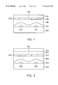
- FIG. 1 is a schematic, cross-sectional view illustrating a semiconductor image sensor in prior art
- FIG. 2 shows transmittance of silicon nitride when the light passes through the silicon nitride layer via a blue color filter
- FIG. 3 is a schematic, cross-sectional view illustrating a semiconductor image sensor in a first preferred embodiment according to the invention
- FIG. 4 shows transmittance of SOG when the light passes into the SOG through a blue color filter
- FIG. 5 shows transmittance of silicon-oxy-nitride layer when light passes through
- FIG. 6 is a schematic, cross-sectional view illustrating a semiconductor image sensor in a second preferred embodiment according to the invention.
- FIG. 3 shows a schematic, cross-sectional view illustrating a semiconductor image sensor fabricated according to this invention.
- a sensor (not shown) including light-receiving portions and electric charge transfer portions such as CMOS fabricated by integrated circuit technology is formed on a semiconductor substrate 300 .
- a metal layer 302 such as an interconnect, is formed over the semiconductor substrate 300 .
- An oxide layer 304 such as silicon-rich oxide (SRO) or PSG is formed by chemical vapor deposition (CVD), for example, over the metal layer 302 to serve as a part of a passivation layer.
- the passivation layer is used to prevent the underlying device from being mechanically damaged and penetrated by moisture and alkaloid ions. Simultaneously, the oxide layer 304 also improves adhesion between the semiconductor substrate 300 , the metal layer 302 and material in subsequent process.
- a spin-on-glass (SOG) 306 is then spun and coated on the oxide layer 304 with suitable solvent in which the 506 can be silicate or siloxane, for example.
- Liquid SOG 306 with high fluidity is employed for spin coating, so that a planar surface is provided over the oxide layer 304 by the SOG 306 .
- an etching back step is performed and, as a result, an even topography is obtained on the SOG 306 .
- the SOG 306 is not only used for a planarized material.
- the transmittance of the SOG 306 with blue light reaches 86% as the light passes through a blue color filter to then pass through the SOG 306 , as indicated by curve 400 in FIG. 4 . Therefore, the transmittance of the SOG 306 with blue light is raised by approximately 20% compared with the transmittance of the silicon nitride in prior art. Additionally, the SOG 306 is capable of anti-reflection and it is not difficult to etch the SOG 306 , such that it can replace the plain film 106 (FIG. 1) in prior art for use as a preferred planarized material in present invention.
- a color filter 312 such as blue color filter is then formed on the SOG 306 .
- Blue light is capable of passing through the material underlying the color filter 312 to the semiconductor substrate 300 when the light penetrates the blue color filter 312 , as shown in FIG. 3 .
- a boron-phosphorus-silicate (BPSG) 314 and a silicon-oxy-nitride layer 316 are successively formed on the color filter 312 .
- the silicon-oxy-nitride layer 310 with a thickness of about 7000 angstroms is formed by chemical vapor deposition using SiH 4 , N 2 O and N 2 as a gas source.
- the formation of the BPSG 314 improves the adhesion between the silicon-oxy-nitride layer 316 and the color filter 312 .
- the silicon-oxy-nitride layer 316 not only functions as water proofing but also protects the color filter 312 from being damaged when the SOG 306 and the oxide layer 304 are etched to expose the bonding pad.
- the transmittance of siliconoxy-nitride layer 310 for light reaches 100%, as indicated by curve 500 in FIG. 5 . Additionally, oxygen is released from the silicon-oxy-nitride layer 310 , such that some cleaning processes are easily performed.
- the transmittance of the SOG 306 with blue light in this invention is higher than that of the silicon nitride layer in prior art and the transmittance of the silicon-oxy-nitride layer 310 with light is higher than that of the plain film, the total transmittance of the silicon-oxy-nitride layer 310 and SOG 306 approaches 86%.
- the transmittance of the structure fabricated in this invention is increased, such that the light which arrives at the semiconductor substrate 300 is strong enough to induce sufficient current and the right information is therefore transmitted, so that the color is preserved.
- the thicknesses of the silicon-oxy-nitride layer 316 and the SOG 306 are thinner than those of the silicon nitride and the plain film in prior art and there is no problem with the etching process such as that used for etching polyimide. Accordingly, the etching time for etching these layers to expose the bonding pad (not shown) is reduced to 2 minutes per wafer and intervals between PMs can be prolonged.
- This invention substitutes a SOG and an oxide layer for the plain film and the silicon nitride layer of conventional art, and a silicon-oxy-nitride layer is formed on the color filter for water proofing, thereby enhancing the blue light transmittance of the semiconductor image sensor by about 20%.
- the etching time is reduced and the interval between PMs is prolonged to shorten fabrication time and lower manufacturing costs. Therefore, this invention is particularly suitable for application in line and quantity production.
- FIG. 6 shows a schematic, cross-sectional view illustrating a semiconductor image sensor fabricated according to this invention.
- a sensor (not shown) including light-receiving portions and electric charge transfer portions such as CMOS fabricated by integrated circuit technology is formed on a semiconductor substrate 600 .
- Metal layer 602 such as an interconnect, is formed over the semiconductor substrate 600 .
- the plain film 604 is also used to prevent the underlying device from being mechanically damaged and penetrated by moisture and alkaloid ions.
- the transmittance of the plain film 604 reaches 81.7% as the light passes through a blue color filter.
- a color filter 606 such as blue color filter is then formed on the plain film 604 .
- Blue light is capable of passing through the material underlying the color filter 606 to the semiconductor substrate 600 when the light penetrates the blue color filter 606 , as shown in FIG. 6 .
- a BPSG 608 and a silicon-oxy-nitride layer 610 are successively formed on the color filter 606 .
- the silicon-oxy-nitride layer 610 with a thickness of about 7000 angstroms is formed by chemical vapor deposition using SiH 4 , N 2 O and N 2 as a gas source.
- the formation of the BPSG 608 improves the adhesion between the silicon-oxy-nitride layer 610 and the color filter 606 .
- the silicon-oxy-nitride layer 610 not only functions as water proofing but also protects the color filter 606 from being damage when the plain film 604 is etched in order to expose the bonding pad.
- the transmittance of the silicon-oxy-nitride layer 610 for light reaches 100%, as indicated by curve 500 in FIG. 5 . Additionally, oxygen is released from the silicon-oxy-nitride layer 610 , such that some cleaning processes are easily performed.
- the transmittance of the plain film 604 with blue light in this invention is higher than that of the silicon nitride layer in prior art and the transmittance of the silicon-oxy-nitride layer 610 reaches 100%, the total transmittance of the silicon-oxy-nitride layer 610 and the plain film 604 approaches 81.7%.
- the transmittance of the structure fabricated in this invention is increased, such that the light which arrives at the semiconductor substrate 600 is strong enough to induce sufficient current and the right information is therefore transmitted, so that the color is preserved.
- the plain film 604 is thinner than the plain films 106 , 110 (FIG. 1) in the prior art, and, as a result, the reaction gas in the chamber is capable of carrying the polymer, suspended in the reaction gas when etching the plain film, out of the chamber.
- the etching time for etching these layers to expose the bonding pad is reduced to 2 minutes per wafer and intervals between PMs can be prolonged.
- This invention substitutes a plain film and a silicon-oxy-nitride for the silicon nitride layer of conventional art, thereby enhancing the blue light transmittance of the semiconductor image sensor by about 18%.
- the etching time is reduced and the interval between PMs is prolonged to shorten fabrication time and lower manufacturing costs. Therefore, this invention is particularly suitable for line production in quantity.
Abstract
A semiconductor image sensor includes a metal layer formed on a semiconductor substrate. An oxide layer is disposed over the semiconductor substrate to cover the metal layer. A SOG is disposed on the oxide layer, a color filter is disposed on the SOG and a silicon-oxy-nitride layer is disposed thereon. By using the high transmittance of the SOG and the silicon-oxy-nitride layer, the blue light transmittance by the semiconductor image sensor is therefore enhanced.
Description
1. Field of the Invention
The invention relates to an image sensor. More particularly, the invention concerns a structure for an image sensor integrated with a semiconductor device having enhanced blue light transmittance.
2. Description of the Related Art
Charge coupled devices (CCD) are currently used as image sensors. CCD technology has been developed over many years and is now mature and stable. Complementary metal oxide semiconductor (CMOS) image sensor technology is newer than CCD technology, and although this newer technology is lower in resolution and quality than a CCD, a CMOS image sensor still has other advantages such as lower fabrication costs due to the use of the CMOS fabrication process.
Although the technology for the CMOS image sensor is not stable and most of processes are still being researched, when compared with the CCD, the CMOS image sensor is more easily integrated with a wafer for purposes such as image processing. Accordingly, the integration of IC devices for a CMOS image sensor can therefore be greatly increased. Fabrication costs are thereby brought down, dimensions are reduced, and power consumption is decreased. All these advantages increase the value of the IC device. Therefore, it is predicted that the CMOS image sensor will take the place of the CCD and play a major role in the future.
However, with respect to a CMOS image sensor, transmittance of light for the semiconductor structure used in a semiconductor image sensor is an important factor seriously influences the quality of the image sensor. For example, it is imperative that the light transmittance is high enough. Only a high transmittance enables the light to arrive at the depletion region with a sufficiently high electric field in the semiconductor substrate. Upon arrival, the transmitted light induces electron-hole pairs due to excitation of photo-energy and thereby produces current in the intrinsic depletion region when light with varied wavelengths penetrates the passivation layer protecting the semiconductor structure.
Referring to FIG. 1, a metal layer 102 is formed over a semiconductor substrate 100 having a CMOS sensor (not shown) to connect with the device on the semiconductor 100. A passivation layer 104 consisting of phosphosilicate glass (PSG) and silicon nitride (SiNx) with a thickness of about 5000 angstroms and about 7000 angstroms, respectively, is formed on the metal layer 102 to protect the underlying devices from being damaged. Due to the formation of devices on the semiconductor substrate 100, and especially to the presence of the metal layer 102, the surface of passivation layer 104 is extremely uneven. It is necessary to form a plain film 106 on the passivation 104 to planarize the passivation layer topography. The plain film 106 can be made from polyimide or acrylic resin, for example, to a thickness of about 16000 angstroms. Thereafter, a color filter 108 is formed on the plain film 106 and light reaches the semiconductor substrate 100 through the color filter 108. A plain film 110 is then formed on the color filter 108 to a thickness of about 10000 angstroms for protecting the color filter 108. Accordingly, the color filter 108 is protected from destruction and contamination by moisture when the etching process for exposing the bonding pad is performed.
Blue light transmittance by the silicon nitride in the passivation layer 104 is about 70% when the light passes through the blue color filter 108, since wavelength of the blue light, about 460 nanometers, is shorter, as shown in FIG. 2. The curve 200 in FIG. 2 represents the transmittance of the silicon nitride when the light passes through the blue color filter to penetrate the silicon nitride. Transmittance of the plain film 104 as the light passes through is about 95%. As a result, the total transmittance of these three films ( plain films 104, 110 and silicon nitride layer) is merely approximately 63.2%. Because the blue light transmits the silicon nitride so poorly, the semiconductor substrate 100 receives insufficient light, which light is incapable of exciting enough electrons. This causes the color to change to yellow. In addition, since the plain film itself is made from polymeric material, polymer is easily produced and covers the wafer when etching the plain film 104 and passivation layer 104 to expose the bonding pad. The etching rate of the layers obviously decreases when the polymer covers the layers that need to be etched. Also, the plain films 106 and 110 are respectively almost 16000 and 10000 angstroms thick, and polymer suspended in the etching gas, such as oxygen, for example, cannot be entirely carried out of the etching chamber by the etching gas when the etching gas is evacuated. . For these reasons, the etching process is conducted with difficulty. Accordingly, the etching process for the wafer requires at least 6 minutes and preventive maintenance (PM) to keep the reaction chamber clean is required after etching 15 wafers. The etching time is too long, the interval between preventive maintenances (PMs) is too short and etchant for etching the plain film 106 is also expensive, so there is no potential for using this process to fabricate a semiconductor image sensor in line and produce product in quantity.
This invention therefore provides a semiconductor image sensor whose blue light transmittance is enhanced.
The invention also provides a semiconductor image sensor that can reduce the etching time and prolong the interval between the PMs. As a result, the manufacturing cost is lowered and the semiconductor image sensor is suitable for line production in quantity.
As embodied and broadly described herein, the invention provides a semiconductor image sensor including a semiconductor substrate having a metal layer. An oxide layer is disposed on the semiconductor substrate to cover the metal layer. A spin on glass (SOG) covers the oxide layer. A color filter is disposed on the SOG, and a silicon-oxy-nitride layer (SiOxNy) is disposed on the color filter.
As embodied and broadly described herein, the invention provides a semiconductor image sensor including a semiconductor substrate having a metal layer. A plain film is disposed on the semiconductor substrate to cover the metal layer. A color filter is disposed on the plain film, and a silicon-oxy-nitride layer (SiOxNy) is disposed on the color filter.
This invention utilizes a silicon-oxy-nitride layer and a SOG with high transmittance to replace the silicon nitride of the passivation layer and the plain film in prior art. Not only the transmittance of the semiconductor image sensor is enhanced, but also the topography of the films underlying the color filter is planar.
It is to be understood that both the foregoing general description and the following detailed description are exemplary and explanatory only and are not restrictive of the invention, as claimed.
The accompanying drawings are included to provide a further understanding of the invention, and are incorporated in and constitute a part of this specification. The drawings illustrate embodiments of the invention and, together with the description, serve to explain the principles of the invention. In the drawings,
FIG. 1 is a schematic, cross-sectional view illustrating a semiconductor image sensor in prior art;
FIG. 2 shows transmittance of silicon nitride when the light passes through the silicon nitride layer via a blue color filter;
FIG. 3 is a schematic, cross-sectional view illustrating a semiconductor image sensor in a first preferred embodiment according to the invention;
FIG. 4 shows transmittance of SOG when the light passes into the SOG through a blue color filter;
FIG. 5 shows transmittance of silicon-oxy-nitride layer when light passes through; and
FIG. 6 is a schematic, cross-sectional view illustrating a semiconductor image sensor in a second preferred embodiment according to the invention;
Reference will now be made in detail to the present preferred embodiments of the invention, examples of which are illustrated in the accompanying drawings. Wherever possible, the same reference numbers are used in the drawings and the description to refer to the same or like parts.
FIRST EMBODIMENT
FIG. 3 shows a schematic, cross-sectional view illustrating a semiconductor image sensor fabricated according to this invention. A sensor (not shown) including light-receiving portions and electric charge transfer portions such as CMOS fabricated by integrated circuit technology is formed on a semiconductor substrate 300. A metal layer 302, such as an interconnect, is formed over the semiconductor substrate 300. An oxide layer 304 such as silicon-rich oxide (SRO) or PSG is formed by chemical vapor deposition (CVD), for example, over the metal layer 302 to serve as a part of a passivation layer. The passivation layer is used to prevent the underlying device from being mechanically damaged and penetrated by moisture and alkaloid ions. Simultaneously, the oxide layer 304 also improves adhesion between the semiconductor substrate 300, the metal layer 302 and material in subsequent process.
A spin-on-glass (SOG) 306 is then spun and coated on the oxide layer 304 with suitable solvent in which the 506 can be silicate or siloxane, for example. Liquid SOG 306 with high fluidity is employed for spin coating, so that a planar surface is provided over the oxide layer 304 by the SOG 306. In order to obtain a desired thickness and uniformity of the me6 306, it is necessary to spin coat SOG 306 to a thickness of 2000 angstroms, twice. After the SOG 306 is formed, an etching back step is performed and, as a result, an even topography is obtained on the SOG 306. However, the SOG 306 is not only used for a planarized material. The transmittance of the SOG 306 with blue light reaches 86% as the light passes through a blue color filter to then pass through the SOG 306, as indicated by curve 400 in FIG. 4. Therefore, the transmittance of the SOG 306 with blue light is raised by approximately 20% compared with the transmittance of the silicon nitride in prior art. Additionally, the SOG 306 is capable of anti-reflection and it is not difficult to etch the SOG 306, such that it can replace the plain film 106 (FIG. 1) in prior art for use as a preferred planarized material in present invention.
With fiiter reference to FIG. 3, a color filter 312, such as blue color filter is then formed on the SOG 306. Blue light is capable of passing through the material underlying the color filter 312 to the semiconductor substrate 300 when the light penetrates the blue color filter 312, as shown in FIG. 3. Thereafter, a boron-phosphorus-silicate (BPSG) 314 and a silicon-oxy-nitride layer 316 are successively formed on the color filter 312. The silicon-oxy-nitride layer 310 with a thickness of about 7000 angstroms is formed by chemical vapor deposition using SiH4, N2O and N2 as a gas source. The formation of the BPSG 314 improves the adhesion between the silicon-oxy-nitride layer 316 and the color filter 312. The silicon-oxy-nitride layer 316 not only functions as water proofing but also protects the color filter 312 from being damaged when the SOG 306 and the oxide layer 304 are etched to expose the bonding pad. The transmittance of siliconoxy-nitride layer 310 for light reaches 100%, as indicated by curve 500 in FIG. 5. Additionally, oxygen is released from the silicon-oxy-nitride layer 310, such that some cleaning processes are easily performed.
Since the transmittance of the SOG 306 with blue light in this invention is higher than that of the silicon nitride layer in prior art and the transmittance of the silicon-oxy-nitride layer 310 with light is higher than that of the plain film, the total transmittance of the silicon-oxy-nitride layer 310 and SOG 306 approaches 86%. As a result, the transmittance of the structure fabricated in this invention is increased, such that the light which arrives at the semiconductor substrate 300 is strong enough to induce sufficient current and the right information is therefore transmitted, so that the color is preserved.
The thicknesses of the silicon-oxy-nitride layer 316 and the SOG 306 are thinner than those of the silicon nitride and the plain film in prior art and there is no problem with the etching process such as that used for etching polyimide. Accordingly, the etching time for etching these layers to expose the bonding pad (not shown) is reduced to 2 minutes per wafer and intervals between PMs can be prolonged.
This invention substitutes a SOG and an oxide layer for the plain film and the silicon nitride layer of conventional art, and a silicon-oxy-nitride layer is formed on the color filter for water proofing, thereby enhancing the blue light transmittance of the semiconductor image sensor by about 20%. In addition, the etching time is reduced and the interval between PMs is prolonged to shorten fabrication time and lower manufacturing costs. Therefore, this invention is particularly suitable for application in line and quantity production.
SECOND EMBODIMENT
FIG. 6 shows a schematic, cross-sectional view illustrating a semiconductor image sensor fabricated according to this invention. A sensor (not shown) including light-receiving portions and electric charge transfer portions such as CMOS fabricated by integrated circuit technology is formed on a semiconductor substrate 600. Metal layer 602, such as an interconnect, is formed over the semiconductor substrate 600. A plain film 604 made of polyimide or acrylic resin, for example, is formed over the metal layer to a thickness of about 16000 angstroms to planarize the uneven topography formed due to the presence of metal layer 602. The plain film 604 is also used to prevent the underlying device from being mechanically damaged and penetrated by moisture and alkaloid ions. The transmittance of the plain film 604 reaches 81.7% as the light passes through a blue color filter.
With further reference to FIG. 6, a color filter 606, such as blue color filter is then formed on the plain film 604. Blue light is capable of passing through the material underlying the color filter 606 to the semiconductor substrate 600 when the light penetrates the blue color filter 606, as shown in FIG. 6. Thereafter, a BPSG 608 and a silicon-oxy-nitride layer 610 are successively formed on the color filter 606. The silicon-oxy-nitride layer 610 with a thickness of about 7000 angstroms is formed by chemical vapor deposition using SiH4, N2O and N2 as a gas source. The formation of the BPSG 608 improves the adhesion between the silicon-oxy-nitride layer 610 and the color filter 606. The silicon-oxy-nitride layer 610 not only functions as water proofing but also protects the color filter 606 from being damage when the plain film 604 is etched in order to expose the bonding pad. The transmittance of the silicon-oxy-nitride layer 610 for light reaches 100%, as indicated by curve 500 in FIG. 5. Additionally, oxygen is released from the silicon-oxy-nitride layer 610, such that some cleaning processes are easily performed.
Since the transmittance of the plain film 604 with blue light in this invention is higher than that of the silicon nitride layer in prior art and the transmittance of the silicon-oxy-nitride layer 610 reaches 100%, the total transmittance of the silicon-oxy-nitride layer 610 and the plain film 604 approaches 81.7%. As a result, the transmittance of the structure fabricated in this invention is increased, such that the light which arrives at the semiconductor substrate 600 is strong enough to induce sufficient current and the right information is therefore transmitted, so that the color is preserved.
The plain film 604 is thinner than the plain films 106, 110 (FIG. 1) in the prior art, and, as a result, the reaction gas in the chamber is capable of carrying the polymer, suspended in the reaction gas when etching the plain film, out of the chamber.
Accordingly, there is no problem with the etching process. Therefore, the etching time for etching these layers to expose the bonding pad (not shown) is reduced to 2 minutes per wafer and intervals between PMs can be prolonged.
This invention substitutes a plain film and a silicon-oxy-nitride for the silicon nitride layer of conventional art, thereby enhancing the blue light transmittance of the semiconductor image sensor by about 18%. In addition, the etching time is reduced and the interval between PMs is prolonged to shorten fabrication time and lower manufacturing costs. Therefore, this invention is particularly suitable for line production in quantity.
Other embodiments of the invention will appear to those skilled in the art from consideration of the specification and practice of the invention disclosed herein. It is intended that the specification and examples be considered as exemplary only, with a true scope and spirit of the invention being indicated by the following claims.
Claims (10)
1. A semiconductor image sensor, comprising:
a semiconductor substrate having a metal layer;
an oxide layer, formed over the semiconductor substrate to cover the metal layer;
a spin-on-glass (SOG), formed on the oxide layer to planarize the oxide layer;
a color filter, formed on the SOG; and
a silicon-oxy-nitride layer, formed on the color filter.
2. The structure according to claim 1, further comprising a boron-phosphorus-silicate glass (BPSG) disposed between the color filter and the silicon-oxy-nitride layer.
3. The structure according to claim 1, wherein the oxide layer includes silicon-rich oxide.
4. The structure according to claim 1, wherein the color filter includes a blue color filter.
5. The structure according to claim 4, wherein a transmittance of the spin-on-glass is approximately 86% as the light passes through the spin-on-glass via the blue color filter.
6. A semiconductor image sensor, comprising:
a semiconductor substrate having a metal layer;
a plain film, formed on the semiconductor substrate to cover the metal layer
a color filter, formed on the plain film; and
a silicon-oxy-nitride layer, formed on the color filter.
7. The structure according to claim 6, further comprising a BPSG disposed between the color filter and the silicon-oxy-nitride layer.
8. The structure according to claim 6, wherein the color filter includes a blue color filter.
9. The structure according to claim 8, wherein a transmittance of the plain film is approximately 81.7% when light passes through the plain film via the blue color filter.
10. The structure according to claim 6, wherein the plain film is about 16000 angstroms thick.
Priority Applications (2)
| Application Number | Priority Date | Filing Date | Title |
|---|---|---|---|
| TW088108619A TW409397B (en) | 1999-05-26 | 1999-05-26 | The structure of semiconductor image sensor and the manufacture method of the same |
| US09/325,031 US6242730B1 (en) | 1999-05-26 | 1999-06-03 | Semiconductor color image sensor |
Applications Claiming Priority (2)
| Application Number | Priority Date | Filing Date | Title |
|---|---|---|---|
| TW088108619A TW409397B (en) | 1999-05-26 | 1999-05-26 | The structure of semiconductor image sensor and the manufacture method of the same |
| US09/325,031 US6242730B1 (en) | 1999-05-26 | 1999-06-03 | Semiconductor color image sensor |
Publications (1)
| Publication Number | Publication Date |
|---|---|
| US6242730B1 true US6242730B1 (en) | 2001-06-05 |
Family
ID=26666695
Family Applications (1)
| Application Number | Title | Priority Date | Filing Date |
|---|---|---|---|
| US09/325,031 Expired - Lifetime US6242730B1 (en) | 1999-05-26 | 1999-06-03 | Semiconductor color image sensor |
Country Status (2)
| Country | Link |
|---|---|
| US (1) | US6242730B1 (en) |
| TW (1) | TW409397B (en) |
Cited By (13)
| Publication number | Priority date | Publication date | Assignee | Title |
|---|---|---|---|---|
| KR20030002881A (en) * | 2001-06-30 | 2003-01-09 | 주식회사 하이닉스반도체 | Image sensor |
| US20030038293A1 (en) * | 2001-08-23 | 2003-02-27 | Duane Fasen | Bottom antireflection coating color filter process for fabricating solid state image sensors |
| US6566151B2 (en) * | 2001-06-21 | 2003-05-20 | United Microelectronics Corp. | Method of forming a color filter |
| US20040080007A1 (en) * | 2002-10-25 | 2004-04-29 | Katsumi Yamamoto | Image sensor having reduced stress color filters and method of making |
| US20040164229A1 (en) * | 2001-03-08 | 2004-08-26 | Xerox Corporation | Color filter configuration for a silicon wafer to be diced into photosensitive chips |
| WO2005119792A1 (en) * | 2004-05-27 | 2005-12-15 | Foveon, Inc. | Vertical color filter sensor group |
| US20060068586A1 (en) * | 2004-09-17 | 2006-03-30 | Bedabrata Pain | Method for implementation of back-illuminated CMOS or CCD imagers |
| EP1677354A1 (en) * | 2004-12-30 | 2006-07-05 | DongbuAnam Semiconductor Inc. | CMOS image sensor and method for manufacturing the same |
| US20060146230A1 (en) * | 2004-12-30 | 2006-07-06 | Dongbuanam Semiconductor Inc. | Image sensor and method of fabricating the same |
| KR100902595B1 (en) | 2007-09-19 | 2009-06-11 | 주식회사 동부하이텍 | Cmos image sensor and method for fabricating of the same |
| US7749799B2 (en) | 2005-11-15 | 2010-07-06 | California Institute Of Technology | Back-illuminated imager and method for making electrical and optical connections to same |
| WO2010117123A2 (en) * | 2009-04-09 | 2010-10-14 | Cheil Industries Inc. | Image sensor and method for manufacturing the same |
| US20110006386A1 (en) * | 2009-07-09 | 2011-01-13 | Cheil Industries Inc. | Organic-Inorganic Hybrid Composition and Image Sensor |
Citations (1)
| Publication number | Priority date | Publication date | Assignee | Title |
|---|---|---|---|---|
| US5796154A (en) * | 1995-05-22 | 1998-08-18 | Matsushita Electronics Corporation | Solid-state imaging device with dual lens structure |
-
1999
- 1999-05-26 TW TW088108619A patent/TW409397B/en not_active IP Right Cessation
- 1999-06-03 US US09/325,031 patent/US6242730B1/en not_active Expired - Lifetime
Patent Citations (1)
| Publication number | Priority date | Publication date | Assignee | Title |
|---|---|---|---|---|
| US5796154A (en) * | 1995-05-22 | 1998-08-18 | Matsushita Electronics Corporation | Solid-state imaging device with dual lens structure |
Cited By (31)
| Publication number | Priority date | Publication date | Assignee | Title |
|---|---|---|---|---|
| US20040164229A1 (en) * | 2001-03-08 | 2004-08-26 | Xerox Corporation | Color filter configuration for a silicon wafer to be diced into photosensitive chips |
| US6998595B2 (en) * | 2001-03-08 | 2006-02-14 | Xerox Corporation | Color filter configuration for a silicon wafer to be diced into photosensitive chips |
| US6566151B2 (en) * | 2001-06-21 | 2003-05-20 | United Microelectronics Corp. | Method of forming a color filter |
| KR20030002881A (en) * | 2001-06-30 | 2003-01-09 | 주식회사 하이닉스반도체 | Image sensor |
| US20030038293A1 (en) * | 2001-08-23 | 2003-02-27 | Duane Fasen | Bottom antireflection coating color filter process for fabricating solid state image sensors |
| US20040002178A1 (en) * | 2001-08-23 | 2004-01-01 | Duane Fasen | Bottom antireflection coating color filter process for fabricating solid state image sensors |
| US6967073B2 (en) | 2001-08-23 | 2005-11-22 | Agilent Technologies, Inc. | Bottom antireflection coating color filter process for fabricating solid state image sensors |
| US20040080007A1 (en) * | 2002-10-25 | 2004-04-29 | Katsumi Yamamoto | Image sensor having reduced stress color filters and method of making |
| US6800838B2 (en) * | 2002-10-25 | 2004-10-05 | Omnivision International Holding Ltd | Image sensor having reduced stress color filters and method of making |
| WO2005119792A1 (en) * | 2004-05-27 | 2005-12-15 | Foveon, Inc. | Vertical color filter sensor group |
| CN1943041B (en) * | 2004-05-27 | 2012-05-16 | 佛文恩股份有限公司 | Vertical color filter sensor group |
| US7615808B2 (en) * | 2004-09-17 | 2009-11-10 | California Institute Of Technology | Structure for implementation of back-illuminated CMOS or CCD imagers |
| US7425460B2 (en) | 2004-09-17 | 2008-09-16 | California Institute Of Technology | Method for implementation of back-illuminated CMOS or CCD imagers |
| US20060068586A1 (en) * | 2004-09-17 | 2006-03-30 | Bedabrata Pain | Method for implementation of back-illuminated CMOS or CCD imagers |
| US20060076590A1 (en) * | 2004-09-17 | 2006-04-13 | Bedabrata Pain | Structure for implementation of back-illuminated CMOS or CCD imagers |
| EP1677354A1 (en) * | 2004-12-30 | 2006-07-05 | DongbuAnam Semiconductor Inc. | CMOS image sensor and method for manufacturing the same |
| US20060146230A1 (en) * | 2004-12-30 | 2006-07-06 | Dongbuanam Semiconductor Inc. | Image sensor and method of fabricating the same |
| US20060145217A1 (en) * | 2004-12-30 | 2006-07-06 | Dongbuanam Semiconductor Inc. | CMOS image sensor and method for manufacturing the same |
| US7442572B2 (en) | 2004-12-30 | 2008-10-28 | Dongbu Electronic Co., Ltd. | CMOS image sensor and method for manufacturing the same |
| US7445950B2 (en) * | 2004-12-30 | 2008-11-04 | Dongbu Electronics Co., Ltd. | Image sensor and method of fabricating the same |
| US20090026357A1 (en) * | 2004-12-30 | 2009-01-29 | Joon Hwang | Image sensor and method of fabricating the same |
| US20090072283A1 (en) * | 2004-12-30 | 2009-03-19 | Hyun Joon Sohn | CMOS image sensor and method for manufacturing the same |
| US7732746B2 (en) | 2004-12-30 | 2010-06-08 | Dongbu Electronics Co., Ltd. | Image sensor and method of fabricating the same |
| US7745862B2 (en) | 2004-12-30 | 2010-06-29 | Dongbu Electronics Co., Ltd. | CMOS image sensor and method for manufacturing the same |
| US7749799B2 (en) | 2005-11-15 | 2010-07-06 | California Institute Of Technology | Back-illuminated imager and method for making electrical and optical connections to same |
| KR100902595B1 (en) | 2007-09-19 | 2009-06-11 | 주식회사 동부하이텍 | Cmos image sensor and method for fabricating of the same |
| WO2010117123A2 (en) * | 2009-04-09 | 2010-10-14 | Cheil Industries Inc. | Image sensor and method for manufacturing the same |
| WO2010117123A3 (en) * | 2009-04-09 | 2011-06-23 | Cheil Industries Inc. | Image sensor and method for manufacturing the same |
| US8502334B2 (en) | 2009-04-09 | 2013-08-06 | Cheil Industries Inc. | Image sensor and method for manufacturing the same |
| US20110006386A1 (en) * | 2009-07-09 | 2011-01-13 | Cheil Industries Inc. | Organic-Inorganic Hybrid Composition and Image Sensor |
| US8487030B2 (en) | 2009-07-09 | 2013-07-16 | Cheil Industries Inc. | Organic-inorganic hybrid composition and image sensor |
Also Published As
| Publication number | Publication date |
|---|---|
| TW409397B (en) | 2000-10-21 |
Similar Documents
| Publication | Publication Date | Title |
|---|---|---|
| US7695995B2 (en) | Image sensor and method of fabricating the same | |
| US6242730B1 (en) | Semiconductor color image sensor | |
| KR100753391B1 (en) | cmos image sensor | |
| US20130153901A1 (en) | BSI Image Sensor Chips and Methods for Forming the Same | |
| KR100674986B1 (en) | Image sensor and method of manufacturing the same | |
| US7713777B2 (en) | Method for manufacturing image sensor | |
| US8101452B2 (en) | Image sensor and method for manufacturing the same | |
| US6396089B1 (en) | Semiconductor image sensor | |
| US7585691B2 (en) | Solid-state imaging device and method for producing the same | |
| US6916680B2 (en) | Method for fabricating image sensor | |
| US7411276B2 (en) | Photosensitive device | |
| US5904558A (en) | Fabrication process of semiconductor device | |
| US7446386B2 (en) | Optical color sensor system | |
| JPH11121725A (en) | Solid-state image pick-up device and its manufacturing method | |
| CN102403324B (en) | The manufacture method of semiconductor device, semiconductor device and photomoduel | |
| US7944014B2 (en) | Image sensor | |
| JP3430759B2 (en) | Method for manufacturing solid-state imaging device and solid-state imaging device | |
| KR100489351B1 (en) | Manufacturing method of image sensor with protective film to which planarization process is applied | |
| US20070166868A1 (en) | Method of fabricating an image sensor | |
| KR20010061343A (en) | Method for fabricating image sensor | |
| US7642119B2 (en) | Method for manufacturing image sensor | |
| US5591680A (en) | Formation methods of opaque or translucent films | |
| US20080073735A1 (en) | Image sensor and fabrication method thereof | |
| JP3626252B2 (en) | Method for manufacturing solid-state imaging device | |
| TW409420B (en) | The image sensor structure and the manufacture method thereof |
Legal Events
| Date | Code | Title | Description |
|---|---|---|---|
| AS | Assignment |
Owner name: UNITED MICROELECTRONICS CORP., TAIWAN Free format text: ASSIGNMENT OF ASSIGNORS INTEREST;ASSIGNORS:LIN, SHIH-YAO;CHEN, SHU-LI;YEH, JEENH-BANG;AND OTHERS;REEL/FRAME:010026/0870;SIGNING DATES FROM 19990518 TO 19990519 |
|
| STCF | Information on status: patent grant |
Free format text: PATENTED CASE |
|
| FPAY | Fee payment |
Year of fee payment: 4 |
|
| FPAY | Fee payment |
Year of fee payment: 8 |
|
| FPAY | Fee payment |
Year of fee payment: 12 |