US6151150A - Method and apparatus for level decision and optical receiver using same - Google Patents
Method and apparatus for level decision and optical receiver using same Download PDFInfo
- Publication number
- US6151150A US6151150A US08/942,619 US94261997A US6151150A US 6151150 A US6151150 A US 6151150A US 94261997 A US94261997 A US 94261997A US 6151150 A US6151150 A US 6151150A
- Authority
- US
- United States
- Prior art keywords
- signal
- voltage
- negative
- positive
- peak
- Prior art date
- Legal status (The legal status is an assumption and is not a legal conclusion. Google has not performed a legal analysis and makes no representation as to the accuracy of the status listed.)
- Expired - Fee Related
Links
Images


Classifications
-
- H—ELECTRICITY
- H04—ELECTRIC COMMUNICATION TECHNIQUE
- H04B—TRANSMISSION
- H04B10/00—Transmission systems employing electromagnetic waves other than radio-waves, e.g. infrared, visible or ultraviolet light, or employing corpuscular radiation, e.g. quantum communication
- H04B10/60—Receivers
- H04B10/66—Non-coherent receivers, e.g. using direct detection
- H04B10/69—Electrical arrangements in the receiver
- H04B10/695—Arrangements for optimizing the decision element in the receiver, e.g. by using automatic threshold control
Definitions
- the present invention relates to a signal transmission system, and more particularly to a level decision circuit used in a signal receiver.
- the PDS Passive Double Star
- AGC Automatic Gain Control
- ATC Automatic Threshold Control
- Such an optical receiver includes a level decision circuit, which decides the level of the input signal to generate a digital output signal of zero or one.
- burst mode signals are transmitted from a transmitter to the optical receiver.
- PON Passive Optical Network
- it is required to start a level decision operation within the first several bits in the burst mode signal.
- a conventional level decision circuit in order to maintain a high transmission rate, the structure of the circuitry becomes complicated. Further, the duty ratio becomes worse and an output error may occur frequently.
- an object of the invention is to provide method and apparatus for level decision which is easily designed to be simple so as to realize a quick start of a level decision process without duty distortion and without output errors.
- Another object of the invention is to provide an optical receiver in which a level decision circuit is designed to be simple so as to realize a quick start of a level decision process without duty distortion and without output errors.
- a method for deciding the level of an input signal includes the step of providing positive and negative signals in response to the input signal.
- the method further includes the steps of: detecting a peak of the positive signal to provide a positive-peak value; detecting a peak of the negative signal to provide a negative-peak value; combining the positive signal and the negative-peak value to provide a first combination signal; and combining the negative signal and the positive-peak value to provide a second combination signal.
- the method still further includes the step of comparing the first and second combination signals to provide an output signal of zero or one.
- a level decision circuit includes a differential amplifier which generates positive and negative signals in response to an input signal; a first peak detector which detects a peak of the positive signal to provide a positive-peak value; and a second peak detector which detects a peak of the negative signal to provide a negative-peak value.
- the circuit further includes a first adder which combines the positive signal and the negative-peak value to provide a first combination signal; and a second adder which combines the negative signal and the positive-peak value to provide a second combination signal.
- the circuit still further includes a comparator which compares the first and second combination signals to provide an output signal of zero or one.
- an optical receiver which generates an electrical digital signal from an optical signal, includes an O/E converter which converts the optical signal into an electrical input signal and a level decision circuit, which includes the same elements as the second aspect of the invention.
- FIG. 1 is a circuit diagram showing a conventional level decision circuit using an AGC scheme.
- FIG. 2 is a circuit diagram showing another conventional level decision circuit using an ATC scheme.
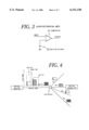
- FIG. 3 is a circuit diagram showing still another conventional level decision circuit.
- FIG. 4 is an explanatory view showing a PON system.
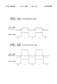
- FIGS. 5A and 5B are timing charts showing the operation of the conventional level decision circuit shown in FIG. 3.
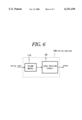
- FIG. 6 is a block diagram showing an optical receiver to which the invention is applied.
- FIG. 7 is a circuit diagram showing the structure of a level decision circuit according to a first preferred embodiment of the invention.
- FIG. 8 is a timing chart showing the operation of the first preferred embodiment.
- FIG. 9 is a circuit diagram showing the structure of a level decision circuit according to a second preferred embodiment of the invention.
- FIG. 1 shows a conventional level decision circuit using an AGC (Automatic Gain Control) scheme, which is generally mounted in an optical receiver.
- the level decision circuit includes a gain-variable amplifier 1, which receives an input signal and amplifies it in accordance with a controlled gain level.
- the gain-variable amplifier 1 is connected at an output terminal to a peak detector 2, which detects a peak voltage "Vpk" of the output signal of the gain-variable amplifier 1, and to an input terminal of a comparator 5.
- the peak detector 2 is connected at an output terminal to an input terminal of an operational amplifier 3, of which the other input terminal is connected to a control voltage source 7.
- the operational amplifier 3 compares the peak voltage "Vpk” and a control voltage "Vagc,” supplied from the control voltage source 7, to generate a gain control signal so that the peak voltage "Vpk” approximates the control voltage "Vagc.”
- the operational amplifier 3 is connected at an output terminal to a time constant circuit 4, which generates a time constant " ⁇ a" for gain control of the gain-variable amplifier 1.
- the time constant circuit 4 is connected at an output terminal to the gain-variable amplifier 1.
- the gain-variable amplifier 1 is also supplied with a reference voltage from a reference voltage source 6.
- the comparator 5 is supplied with a threshold voltage "Vth" from a reference voltage source 8.
- the threshold voltage "Vth” is determined suitably to provide the maximum SIN ratio between the control voltage "Vagc” and the output level of the gain-variable amplifier 1 in the condition of no input.
- the comparator 5 compares the output level of the gain-variable amplifier 1 to the threshold voltage "Vth” to output a digital signal of zero or one.
- FIG. 2 shows another conventional level decision circuit using ATC (Automatic Threshold Control) scheme, which includes a differential amplifier 11 to which an input signal is supplied.
- the differential amplifier 11 is connected at positive and negative output terminals to one end of each of resistors 13 and 14, respectively.
- the resistor 13 is connected at its other end to an input terminal of an operational amplifier 12 and a resistor 15.
- the resistor 14 is connected at its other end to the other input terminal of the operational amplifier 12 and a resistor 16.
- the operational amplifier 12 is connected at positive and negative output terminals to input terminals of a limiter amplifier 18.
- the positive output terminal of the operational amplifier 12 is also connected to a peak detector 17, whose output terminal is connected to one of the input terminals of the operational amplifier 12.
- the other end of the resistor 15 is connected to the input terminal of the limiter amplifier 18, which is also connected to the negative output terminal of the operational amplifier 12.
- the differential amplifier 11 is connected at the other input terminal to a reference voltage source 19, which is grounded.
- FIG. 3 shows another conventional level decision circuit, which includes a comparator 21 to which an input signal is supplied, and a decision voltage source 22 connected to an input terminal of the comparator 21.
- the decision voltage source 22 provides a fixed voltage that is determined to be slightly higher than the minimum level of the input signal.
- the comparator 21 compares the input signal to the decision voltage to generate an output signal of zero or one.
- FIG. 4 shows a PON (Passive Optical Network) system including an optical receiver to which the above-mentioned level decision circuit can be applied.
- PON Passive Optical Network
- burst mode signals are supplied from an optical transmitter.
- the burst mode signals are transmitted through a star coupler and an optical fiber to the optical receiver.
- the burst mode signal is a signal whose level (light power) varies for each time slot. For maintaining a high transmission rate in the PON system, it is required to start a level decision operation within first several bits in the burst mode signal.
- the time constant " ⁇ a" is determined to be very low in order to maintain a high transmission efficiency. Further, it is required that the gain of the gain-variable amplifier 1 and the gain of the operational amplifier 3 are determined to be lower to provide enough phase margin for preventing the occurrence of oscillation. If the gain of the gain-variable amplifier 1 and the operational amplifier 3 are set low, the error between the control voltage "Vagc" and the peak voltage of the output signal of the gain-variable amplifier 1 becomes large. Therefore, a great effort for circuit design is needed.
- the negative feedback is made with the resistors 13 to 16 and the peak detector 17, so that an ATC operation starts quickly.
- it is required to perform phase compensation on the circuitry for preventing the occurrence of oscillation.
- the structure of the circuitry becomes complicated, as in the case of the level decision circuit shown in FIG. 1.
- FIG. 5A shows the relationship between the input signal level and the output signal level when the input signal has a lower amplitude.
- FIG. 5B shows the relationship between the input signal level and the output signal level when the input signal has a higher amplitude.
- the duty distortion appears remarkable when the input signal has a higher amplitude.
- FIG. 6 shows the structure of an optical receiver 100, which includes a PD-AMP module 110 and a level decision circuit 30.
- the PD-AMP module 110 includes a photo-diode, which converts an optical input signal into an electrical signal, and a pre-amplifier, which amplifies the electrical signal.
- the level decision circuit 30 generates a digital output signal in response to the electrical signal supplied from the PD-AMP module 110.
- FIG. 7 shows the structure of the level decision circuit 30, according to a first preferred embodiment of the invention.
- the level decision circuit 30 includes a differential amplifier 31, to which an input signal (electrical signal) "Vin" is supplied.
- the other input terminal of the differential amplifier 31 is connected to a first reference voltage source 37.
- the differential amplifier 31 is connected at a positive output terminal to an input terminal of a first peak detector 32 and an input terminal of a first adder 34.
- a negative output terminal of the differential amplifier 31 is connected to an input terminal of a second peak detector 33 and an input terminal of a second adder 35.
- the first peak detector 32 is connected at an output terminal to another input terminal of the second adder 35.
- the second peak detector 33 is connected at an output terminal to another input terminal of the first adder 34.
- the first adder 34 is connected at the other input terminal to an offset voltage source 39, which is connected to a second reference voltage source 38.
- the second adder 35 is connected at the other input terminal to the second reference voltage source 38.
- the output terminals of the first and second adders 34 and 35 are connected to negative and positive input terminals of a comparator 36, respectively.
- the input signal "Vin” is amplified by the differential amplifier 31 to provide positive and negative signals “Vdata-p” and “Vdata-n,” which have the same amplitude in the opposite logic.
- the first and second peak detectors 32 and 33 detect peak voltage values "Vpk1" and "Vpk2" of the positive signal Vdata-p and negative signal Vdata-n, supplied from the differential amplifier 31, respectively.
- the first adder 34 combines (sums) the positive signal Vdata-p and the peak voltage "Vpk2" using a reference voltage of "Vref2+Voff” to provide a first sum-voltage signal (combination signal) "Vsum1.”
- the second adder 35 combines (sums) the negative signal Vdata-n and the peak signal "Vpk1” using a reference voltage of "Vref2” to provide a second sum-voltage signal (combination signal) "Vsum2.”
- the sum-voltage signal "Vsum1” and “Vsum2” are in the opposite logic to each other, and have bottom levels (offset levels) that differ from each other by 2Voff.
- the comparator 36 compares the sum-voltage signals "Vsum1" and “Vsum2" to provide a digital output signal "Vout" of zero or one.
- the offset voltage source 39 provides a micro-offset voltage "Voff” to shift the reference level so that the first sum-voltage signal "Vsum1” becomes 2Voff lower than the second sum-voltage signal “Vsum2.” As a result, the signal level zero is accurately decided (identified).
- the mid-point voltage "Vref2" of the output of the differential amplifier 31 is used as the reference voltage for the summing operation.
- the reference voltage is not limited by the mid-point voltage "Vref2" of the output of the differential amplifier 31, but can be any other voltage in the dynamic range of the adders 34 and 35.
- different types of differential amplifiers, peak detectors and adders can be used. Any values of reference voltages, offset voltage and signal level do not limit the invention.
- the differential amplifier 31, peak detectors 32 and 33, adders 34 and 35, and comparator 36 are serially connected without negative feedback circuits. Therefore, it is easy to design the circuitry simple to realize a quick start of level decision process. Further, the sum-voltage signals "Vsum1" and “Vsum2" have substantially the same bottom level, as shown in FIG. 8, so that the comparator 36 supplies the output signal "Vout” without duty distortion. In addition, even if the offset voltage between the input signal "Vin” and the reference voltage "Vref1" is large, the level decision process can be performed without output errors.
- FIG. 9 shows the structure of a level decision circuit 40, according to a second preferred embodiment of the invention.
- the level decision circuit includes a differential amplifier 41, to which an input signal (electrical signal) "Vin" is supplied.
- the other input terminal of the differential amplifier 31 is connected to a first reference voltage source 47.
- the differential amplifier 41 is connected at a positive output terminal to an input terminal of a first peak detector 42 and to an input terminal of a first adder 44.
- a negative output terminal of the differential amplifier 41 is connected to an input terminal of a second peak detector 43 and to an input terminal of a second adder 45.
- the first peak detector 42 is connected at an output terminal to another input terminal of the second adder 45.
- the second peak detector 43 is connected at an output terminal to another input terminal of the first adder 44.
- the first adder 44 is connected at the other input terminal to a positive output terminal of an operational amplifier 54.
- the second adder 45 is connected at the other input terminal to a negative output terminal of the operational amplifier 54.
- the output terminals of the first and second adders 44 and 45 are connected to negative and positive input terminals of a comparator 46, respectively.
- the first adder 44 is also connected at an output terminal to an input terminal of a voltage detector 51.
- the second adder 45 is also connected at an output terminal to an input terminal of a voltage detector 52.
- the output terminals of the voltage detector 51 and 52 are connected to negative and positive input terminals of a differential amplifier 53, respectively.
- the operational amplifier 54 is connected at input terminals to an output terminal of the differential amplifier 53 and to a second reference voltage source 48.
- the second reference voltage source 48 supplies an offset voltage to sum-voltage signals (combination signals) outputted from the first and second adders 44 and 45.
- the input signal "Vin” is amplified by the differential amplifier 41 to provide positive and negative signals Vdata-p and Vdata-n, which have the same amplitude in the opposite logic.
- the first and second peak detectors 42 and 43 detect peak voltage signals "Vpk1" and “Vpk2" of the positive signal Vdata-p and negative signal Vdata-n, supplied from the differential amplifier 41, respectively.
- the first adder 44 combines (sums) the positive signal Vdata-p, the peak voltage "Vpk2" and “Voff” to provide the sum-voltage signal "Vsum1.”
- the second adder 45 combines the negative signal Vdata-n, the peak voltage "Vpk1” and Voff to provide the sum-voltage signal "Vsum2.”
- the comparator 46 compares the signals "Vsum1” and "Vsum2” to provide a digital output signal "Vout" of zero or one.
- the voltage detectors 51 and 52 detect the output voltages of the first and second adders 44 and 45.
- the differential amplifier 53 generates a feedback voltage in response to the output signals of the voltage detectors 51 and 52.
- the operational amplifier 54 supplies the feedback voltage signals to the first and second adders 44 and 45.
- each of the first and second adders 44 and 45 has a single output, however, each adder may have two output terminals. That is, each adder has positive output terminal and a negative output terminal.
- the first adder 44 may output signals of "Vsum1" and inverted-Vsum1, and the mid-point of the two output signals is generated by a resistance-division technique, or the like. The mid-point voltage is supplied to the differential amplifier.
- a stable offset voltage which is the difference between the signals "Vsum1" and "Vsum2" can be applied to the comparator 46 without affecting a difference in a DC bias between the two adders, which occurs with temperature variation.
- bottom detector circuits may be used instead of the voltage detectors 51 and 52.
- the output signals of the bottom detector circuits are supplied to the differential amplifier.
- a more stable offset voltage which is the difference between the signals "Vsum1" and "Vsum2,” can be provided without affecting the differences in DC bias and gain between the two adders, and other errors.
- the output voltage of the adders 44 and 45 are applied to the differential amplifier 53, and the output of the differential amplifier is supplied to the operational amplifier 54.
- the voltage source 48 provides an offset voltage between the signals "Vsum1" and “Vsum2.”
- the operational amplifier 54 outputs offset voltage signals "Voff” and inverted-Voff, which are supplied to the first and second adders 44 and 45, respectively.
- Such feedback signals function as a micro-offset voltage to shift the reference level when input signals of zero are successively inputted, so that the output signal of zero is accurately outputted. Accordingly, the level decision circuit operates stably even if a signal of zero is inputted.
- the circuitry it is easy to design the circuitry to be simple, to realize a quick start of a level decision process.
- the level decision process can be performed without output errors and duty distortion.
- the level decision circuits 30 and 40 are suitable for an optical receiver of a PON system, which processes burst mode signals whose level (light power) varies for each time slot.
- the invention is applicable to a signal receiver in a LAN (Local Area Network) system using TDMA (Time Division Multiple Access) scheme. Further, the invention is applicable to any kinds of signal receiver which receives digital signals.
Abstract
Description
Claims (3)
Applications Claiming Priority (4)
| Application Number | Priority Date | Filing Date | Title |
|---|---|---|---|
| JP26262496 | 1996-10-03 | ||
| JP8-262624 | 1996-10-03 | ||
| JP04407397A JP3340341B2 (en) | 1996-10-03 | 1997-02-27 | Level identification circuit |
| JP9-044073 | 1997-02-27 |
Publications (1)
| Publication Number | Publication Date |
|---|---|
| US6151150A true US6151150A (en) | 2000-11-21 |
Family
ID=26383921
Family Applications (1)
| Application Number | Title | Priority Date | Filing Date |
|---|---|---|---|
| US08/942,619 Expired - Fee Related US6151150A (en) | 1996-10-03 | 1997-10-02 | Method and apparatus for level decision and optical receiver using same |
Country Status (2)
| Country | Link |
|---|---|
| US (1) | US6151150A (en) |
| JP (1) | JP3340341B2 (en) |
Cited By (41)
| Publication number | Priority date | Publication date | Assignee | Title |
|---|---|---|---|---|
| US20010004388A1 (en) * | 1999-12-15 | 2001-06-21 | Nec Corporation | Offset control circuit, optical receiver using the same and optical communication system |
| US6377633B1 (en) * | 1998-10-09 | 2002-04-23 | Harris Corporation | Apparatus and method for decoding asynchronous data |
| US6587004B2 (en) * | 1999-12-27 | 2003-07-01 | Fujitsu Limited | Signal amplifier and optical signal receiver using the same |
| US6595708B1 (en) * | 1998-12-10 | 2003-07-22 | Opnext Japan, Inc. | Optical receiver circuit and optical module using same in optical communication system |
| US6608710B1 (en) * | 2000-01-31 | 2003-08-19 | Leitch Technology International Inc. | Automatic gain control circuit and optical receiver |
| US20030174023A1 (en) * | 2002-03-12 | 2003-09-18 | Tokio Miyasita | Analog summing and differencing circuit, optical receiving circuit, optical transmitting circuit, automatic gain control amplifier, automatic frequency compensation amplifier, and limiting amplifier |
| US20030190775A1 (en) * | 2002-04-08 | 2003-10-09 | Kim Suk Ki | Infrared remote control receiver (IRCR) having semiconductor signal processing device therein |
| US20030231032A1 (en) * | 2002-06-13 | 2003-12-18 | Takayuki Tanaka | Multistage level discrimination circuit |
| US6671075B1 (en) * | 2002-06-24 | 2003-12-30 | Oki Electric Industry Co., Ltd. | Offset voltage cancellation circuit |
| WO2004014066A2 (en) * | 2002-07-31 | 2004-02-12 | Koninklijke Philips Electronics N.V. | Method and devic the for setting the slice level in a binary signal |
| US20040057725A1 (en) * | 2002-09-23 | 2004-03-25 | Jyung-Chan Lee | Method and apparatus for optimizing decision level of signal output from optical receiver |
| US6735260B1 (en) * | 2000-04-17 | 2004-05-11 | Texas Instruments Incorporated | Adaptive data slicer |
| US6744987B1 (en) * | 2000-04-17 | 2004-06-01 | Delphi Technologies, Inc | Tertiary optical media interface |
| US20040105687A1 (en) * | 2002-11-07 | 2004-06-03 | Myong Seung Il | Method of optimizing output signal of optical receiver using FEC and optical receiving system using the method |
| US6747515B2 (en) * | 2000-04-28 | 2004-06-08 | Stmicroelectronics, Inc. | Circuit for automatic regulation of a differential amplifier's gain |
| US20040208508A1 (en) * | 2002-03-07 | 2004-10-21 | Takayuki Tanaka | Optical signal reception control circuit and method for controlling reception of optical signal |
| US6816101B2 (en) | 2002-03-08 | 2004-11-09 | Quelian, Inc. | High-speed analog-to-digital converter using a unique gray code |
| US20040233090A1 (en) * | 2003-05-22 | 2004-11-25 | Oki Electric Industry Co., Ltd. | Demodulating circuit and optical receiving circuit |
| US20040233047A1 (en) * | 2003-05-23 | 2004-11-25 | King Ronald O. | Clamping circuit for an RF receiver system |
| US20050135818A1 (en) * | 2003-12-18 | 2005-06-23 | Lee Jyung C. | Apparatus for controlling decision threshold voltage to optical receiver |
| US6963696B1 (en) * | 2001-04-30 | 2005-11-08 | Quantum Bridge Communications, Inc. | AC-coupled burst mode receiver with wide dynamic range |
| US20060023518A1 (en) * | 2003-02-27 | 2006-02-02 | Yoshihisa Iwata | Semiconductor apparatus having logic level decision circuit and inter-semiconductor apparatus signal transmission system |
| US20060245520A1 (en) * | 2005-04-28 | 2006-11-02 | Dejan Mijuskovic | Logic threshold acquisition circuits and methods using reversed peak detectors |
| US20070081827A1 (en) * | 2005-10-11 | 2007-04-12 | Fujitsu Limited | Optical receiver for regeneration of optical signal |
| US20070146795A1 (en) * | 2005-12-28 | 2007-06-28 | Fujitsu Limited | Signal light processing apparatus |
| US20090134913A1 (en) * | 2007-11-26 | 2009-05-28 | Faraday Technology Corp. | Signal comparison circuit |
| US20090175623A1 (en) * | 2007-07-27 | 2009-07-09 | Photonic Solution, Inc. | Optical signal detector |
| US20090224804A1 (en) * | 2007-08-07 | 2009-09-10 | Ricoh Company, Ltd. | Detecting circuit and electronic apparatus using detecting circuit |
| US7725079B2 (en) | 2004-12-14 | 2010-05-25 | Quellan, Inc. | Method and system for automatic control in an interference cancellation device |
| US7729431B2 (en) | 2003-11-17 | 2010-06-01 | Quellan, Inc. | Method and system for antenna interference cancellation |
| US20100135678A1 (en) * | 2008-11-28 | 2010-06-03 | Fujitsu Limited | Optical receiving device, optical receiving circuit, and method for receiving optical signals |
| US7804760B2 (en) | 2003-08-07 | 2010-09-28 | Quellan, Inc. | Method and system for signal emulation |
| CN101303795B (en) * | 2002-04-08 | 2010-11-17 | 矽立康通讯科技株式会社 | Infrared remote controller receiver having semiconductor signal processing device designed by only CMOS process |
| US7934144B2 (en) | 2002-11-12 | 2011-04-26 | Quellan, Inc. | High-speed analog-to-digital conversion with improved robustness to timing uncertainty |
| US8005430B2 (en) | 2004-12-14 | 2011-08-23 | Quellan Inc. | Method and system for reducing signal interference |
| US8068406B2 (en) | 2003-08-07 | 2011-11-29 | Quellan, Inc. | Method and system for crosstalk cancellation |
| US8311168B2 (en) | 2002-07-15 | 2012-11-13 | Quellan, Inc. | Adaptive noise filtering and equalization for optimal high speed multilevel signal decoding |
| US8576939B2 (en) | 2003-12-22 | 2013-11-05 | Quellan, Inc. | Method and system for slicing a communication signal |
| US9252983B2 (en) | 2006-04-26 | 2016-02-02 | Intersil Americas LLC | Method and system for reducing radiated emissions from a communications channel |
| WO2017046067A1 (en) * | 2015-09-15 | 2017-03-23 | Firecomms Limited | An optical receiver |
| TWI763555B (en) * | 2021-05-19 | 2022-05-01 | 南亞科技股份有限公司 | Single ended receiver |
Families Citing this family (2)
| Publication number | Priority date | Publication date | Assignee | Title |
|---|---|---|---|---|
| JP4485973B2 (en) * | 2005-02-17 | 2010-06-23 | 株式会社フジクラ | Burst signal receiver |
| JP2006229541A (en) * | 2005-02-17 | 2006-08-31 | Sigma-Links Inc | Burst signal receiving device |
Citations (3)
| Publication number | Priority date | Publication date | Assignee | Title |
|---|---|---|---|---|
| US5025456A (en) * | 1989-02-02 | 1991-06-18 | At&T Bell Laboratories | Burst mode digital data receiver |
| US5612810A (en) * | 1994-09-12 | 1997-03-18 | Nec Corporation | Optical receiving apparatus |
| US5892609A (en) * | 1996-05-24 | 1999-04-06 | Kabushiki Kaisha Toshiba | Digital signal receiver circuit |
-
1997
- 1997-02-27 JP JP04407397A patent/JP3340341B2/en not_active Expired - Fee Related
- 1997-10-02 US US08/942,619 patent/US6151150A/en not_active Expired - Fee Related
Patent Citations (3)
| Publication number | Priority date | Publication date | Assignee | Title |
|---|---|---|---|---|
| US5025456A (en) * | 1989-02-02 | 1991-06-18 | At&T Bell Laboratories | Burst mode digital data receiver |
| US5612810A (en) * | 1994-09-12 | 1997-03-18 | Nec Corporation | Optical receiving apparatus |
| US5892609A (en) * | 1996-05-24 | 1999-04-06 | Kabushiki Kaisha Toshiba | Digital signal receiver circuit |
Cited By (69)
| Publication number | Priority date | Publication date | Assignee | Title |
|---|---|---|---|---|
| US6377633B1 (en) * | 1998-10-09 | 2002-04-23 | Harris Corporation | Apparatus and method for decoding asynchronous data |
| US6595708B1 (en) * | 1998-12-10 | 2003-07-22 | Opnext Japan, Inc. | Optical receiver circuit and optical module using same in optical communication system |
| US20010004388A1 (en) * | 1999-12-15 | 2001-06-21 | Nec Corporation | Offset control circuit, optical receiver using the same and optical communication system |
| US6587004B2 (en) * | 1999-12-27 | 2003-07-01 | Fujitsu Limited | Signal amplifier and optical signal receiver using the same |
| US6608710B1 (en) * | 2000-01-31 | 2003-08-19 | Leitch Technology International Inc. | Automatic gain control circuit and optical receiver |
| US6744987B1 (en) * | 2000-04-17 | 2004-06-01 | Delphi Technologies, Inc | Tertiary optical media interface |
| US6735260B1 (en) * | 2000-04-17 | 2004-05-11 | Texas Instruments Incorporated | Adaptive data slicer |
| US6747515B2 (en) * | 2000-04-28 | 2004-06-08 | Stmicroelectronics, Inc. | Circuit for automatic regulation of a differential amplifier's gain |
| US6963696B1 (en) * | 2001-04-30 | 2005-11-08 | Quantum Bridge Communications, Inc. | AC-coupled burst mode receiver with wide dynamic range |
| US20040208508A1 (en) * | 2002-03-07 | 2004-10-21 | Takayuki Tanaka | Optical signal reception control circuit and method for controlling reception of optical signal |
| US6816101B2 (en) | 2002-03-08 | 2004-11-09 | Quelian, Inc. | High-speed analog-to-digital converter using a unique gray code |
| US7126419B2 (en) | 2002-03-12 | 2006-10-24 | Oki Electric Industry Co., Ltd. | Analog summing and differencing circuit, optical receiving circuit, optical transmitting circuit, automatic gain control amplifier, automatic frequency compensation amplifier, and limiting amplifier |
| US20030174023A1 (en) * | 2002-03-12 | 2003-09-18 | Tokio Miyasita | Analog summing and differencing circuit, optical receiving circuit, optical transmitting circuit, automatic gain control amplifier, automatic frequency compensation amplifier, and limiting amplifier |
| US20030190775A1 (en) * | 2002-04-08 | 2003-10-09 | Kim Suk Ki | Infrared remote control receiver (IRCR) having semiconductor signal processing device therein |
| CN101303795B (en) * | 2002-04-08 | 2010-11-17 | 矽立康通讯科技株式会社 | Infrared remote controller receiver having semiconductor signal processing device designed by only CMOS process |
| CN100421132C (en) * | 2002-04-08 | 2008-09-24 | 矽立康通讯科技株式会社 | Infrared remote control receiver (IRCR) having semiconductor signal processing device |
| US7231152B2 (en) * | 2002-04-08 | 2007-06-12 | Silicon Communications Technology Co., Ltd. | Infrared remote control receiver (IRCR) having semiconductor signal processing device therein |
| US20030231032A1 (en) * | 2002-06-13 | 2003-12-18 | Takayuki Tanaka | Multistage level discrimination circuit |
| US6965257B2 (en) * | 2002-06-13 | 2005-11-15 | Oki Electric Industry Co., Ltd. | Multistage level discrimination circuit |
| US6671075B1 (en) * | 2002-06-24 | 2003-12-30 | Oki Electric Industry Co., Ltd. | Offset voltage cancellation circuit |
| US8311168B2 (en) | 2002-07-15 | 2012-11-13 | Quellan, Inc. | Adaptive noise filtering and equalization for optimal high speed multilevel signal decoding |
| WO2004014066A3 (en) * | 2002-07-31 | 2004-09-02 | Koninkl Philips Electronics Nv | Method and devic the for setting the slice level in a binary signal |
| WO2004014066A2 (en) * | 2002-07-31 | 2004-02-12 | Koninklijke Philips Electronics N.V. | Method and devic the for setting the slice level in a binary signal |
| US7711071B2 (en) | 2002-07-31 | 2010-05-04 | Nxp B.V. | Setting the slice level in a binary signal |
| CN1320753C (en) * | 2002-07-31 | 2007-06-06 | 皇家飞利浦电子股份有限公司 | Method and apparatus for setting the slice level in a binary signal |
| US20060152626A1 (en) * | 2002-07-31 | 2006-07-13 | Koninklijke Philips Electronics, N.V. | Setting the slice level in a binary signal |
| US7298978B2 (en) | 2002-09-23 | 2007-11-20 | Electronics And Telecommunications Research Institute | Method and apparatus for optimizing decision level of signal output from optical receiver |
| US20040057725A1 (en) * | 2002-09-23 | 2004-03-25 | Jyung-Chan Lee | Method and apparatus for optimizing decision level of signal output from optical receiver |
| US7212741B2 (en) | 2002-11-07 | 2007-05-01 | Electronics And Telecommunications Research Institute | Method of optimizing output signal of optical receiver using FEC and optical receiving system using the method |
| US20040105687A1 (en) * | 2002-11-07 | 2004-06-03 | Myong Seung Il | Method of optimizing output signal of optical receiver using FEC and optical receiving system using the method |
| US7934144B2 (en) | 2002-11-12 | 2011-04-26 | Quellan, Inc. | High-speed analog-to-digital conversion with improved robustness to timing uncertainty |
| US20060023518A1 (en) * | 2003-02-27 | 2006-02-02 | Yoshihisa Iwata | Semiconductor apparatus having logic level decision circuit and inter-semiconductor apparatus signal transmission system |
| US7375544B2 (en) * | 2003-02-27 | 2008-05-20 | Kabushiki Kaisha Toshiba | Semiconductor apparatus having logic level decision circuit and inter-semiconductor apparatus signal transmission system |
| US6891900B2 (en) | 2003-05-22 | 2005-05-10 | Oki Electric Industry Co., Ltd. | Demodulating circuit and optical receiving circuit |
| US20040233090A1 (en) * | 2003-05-22 | 2004-11-25 | Oki Electric Industry Co., Ltd. | Demodulating circuit and optical receiving circuit |
| US20040233047A1 (en) * | 2003-05-23 | 2004-11-25 | King Ronald O. | Clamping circuit for an RF receiver system |
| US6914522B2 (en) | 2003-05-23 | 2005-07-05 | Lear Corporation | Clamping circuit for an RF receiver system |
| DE102004024906B4 (en) * | 2003-05-23 | 2006-01-05 | Lear Corporation, Southfield | Clamping circuit for a receiver system |
| US8068406B2 (en) | 2003-08-07 | 2011-11-29 | Quellan, Inc. | Method and system for crosstalk cancellation |
| US8605566B2 (en) | 2003-08-07 | 2013-12-10 | Quellan, Inc. | Method and system for signal emulation |
| US7804760B2 (en) | 2003-08-07 | 2010-09-28 | Quellan, Inc. | Method and system for signal emulation |
| US7729431B2 (en) | 2003-11-17 | 2010-06-01 | Quellan, Inc. | Method and system for antenna interference cancellation |
| US7313333B2 (en) | 2003-12-18 | 2007-12-25 | Electronics And Telecommunications Research Institute | Apparatus for controlling decision threshold voltage to optical receiver |
| US20050135818A1 (en) * | 2003-12-18 | 2005-06-23 | Lee Jyung C. | Apparatus for controlling decision threshold voltage to optical receiver |
| US8576939B2 (en) | 2003-12-22 | 2013-11-05 | Quellan, Inc. | Method and system for slicing a communication signal |
| US8135350B2 (en) | 2004-12-14 | 2012-03-13 | Quellan, Inc. | System for reducing signal interference |
| US8005430B2 (en) | 2004-12-14 | 2011-08-23 | Quellan Inc. | Method and system for reducing signal interference |
| US8503940B2 (en) | 2004-12-14 | 2013-08-06 | Quellan, Inc. | Reducing signal interference |
| US7725079B2 (en) | 2004-12-14 | 2010-05-25 | Quellan, Inc. | Method and system for automatic control in an interference cancellation device |
| US20060245520A1 (en) * | 2005-04-28 | 2006-11-02 | Dejan Mijuskovic | Logic threshold acquisition circuits and methods using reversed peak detectors |
| CN101584168B (en) * | 2005-04-28 | 2012-08-01 | 飞思卡尔半导体公司 | Logic threshold acquisition circuits and methods using reversed peak detectors |
| US7684518B2 (en) * | 2005-04-28 | 2010-03-23 | Freescale Semiconductor, Inc. | Logic threshold acquisition circuits and methods using reversed peak detectors |
| US7809286B2 (en) * | 2005-10-11 | 2010-10-05 | Fujitsu Limited | Optical receiver for regeneration of optical signal |
| US20090232519A1 (en) * | 2005-10-11 | 2009-09-17 | Fujitsu Limited | Optical receiver for regeneration of optical signal |
| US20070081827A1 (en) * | 2005-10-11 | 2007-04-12 | Fujitsu Limited | Optical receiver for regeneration of optical signal |
| US7769304B2 (en) * | 2005-12-28 | 2010-08-03 | Fujitsu Limited | Signal light processing apparatus |
| US20070146795A1 (en) * | 2005-12-28 | 2007-06-28 | Fujitsu Limited | Signal light processing apparatus |
| US9252983B2 (en) | 2006-04-26 | 2016-02-02 | Intersil Americas LLC | Method and system for reducing radiated emissions from a communications channel |
| US7986886B2 (en) * | 2007-07-27 | 2011-07-26 | Wooriro Optical Telecom Co., Ltd. | Optical signal detector |
| US20090175623A1 (en) * | 2007-07-27 | 2009-07-09 | Photonic Solution, Inc. | Optical signal detector |
| US20090224804A1 (en) * | 2007-08-07 | 2009-09-10 | Ricoh Company, Ltd. | Detecting circuit and electronic apparatus using detecting circuit |
| US20090134913A1 (en) * | 2007-11-26 | 2009-05-28 | Faraday Technology Corp. | Signal comparison circuit |
| US7782095B2 (en) * | 2007-11-26 | 2010-08-24 | Faraday Technology Corp. | Signal comparison circuit |
| US8478138B2 (en) * | 2008-11-28 | 2013-07-02 | Fujitsu Limited | Optical receiving device, optical receiving circuit, and method for receiving optical signals |
| US20100135678A1 (en) * | 2008-11-28 | 2010-06-03 | Fujitsu Limited | Optical receiving device, optical receiving circuit, and method for receiving optical signals |
| WO2017046067A1 (en) * | 2015-09-15 | 2017-03-23 | Firecomms Limited | An optical receiver |
| CN108141186A (en) * | 2015-09-15 | 2018-06-08 | 法尔科姆斯有限公司 | Optical receiver |
| US10333472B2 (en) | 2015-09-15 | 2019-06-25 | Firecomms Limited | Optical receiver |
| TWI763555B (en) * | 2021-05-19 | 2022-05-01 | 南亞科技股份有限公司 | Single ended receiver |
Also Published As
| Publication number | Publication date |
|---|---|
| JP3340341B2 (en) | 2002-11-05 |
| JPH10163828A (en) | 1998-06-19 |
Similar Documents
| Publication | Publication Date | Title |
|---|---|---|
| US6151150A (en) | Method and apparatus for level decision and optical receiver using same | |
| US5539779A (en) | Automatic offset control circuit for digital receiver | |
| US5612810A (en) | Optical receiving apparatus | |
| US5581387A (en) | Optical data communications network with a plurality of optical transmitters and a common optical receiver connected via a passive optical network | |
| US6181454B1 (en) | Adaptive threshold controlled decision circuit immune to ringing components of digital signals | |
| JP2991911B2 (en) | Digital data receiver | |
| US5822104A (en) | Digital optical receiving apparatus | |
| US5875049A (en) | Amplifier for burst signal and optical receiving circuit | |
| EP0611059B1 (en) | A system for DC restoration of serially transmitted binary signals | |
| JPH06232916A (en) | Digital data receiver | |
| EP1355464B1 (en) | DC removal in an optical receiver | |
| US7382987B2 (en) | Identification level control method and optical receiver | |
| JP2000174827A (en) | Optical receiving circuit and optical module using the same | |
| JP2002164855A (en) | Optical reception circuit | |
| JP2655130B2 (en) | Digital receiver circuit | |
| EP0868022B1 (en) | Offset correction circuit | |
| JP2962218B2 (en) | Digital optical receiving circuit | |
| US6232842B1 (en) | Amplifying circuit and optical receiver comprising the same | |
| KR100601048B1 (en) | Receiver for burst mode packet and Method for receiving the packet | |
| JPH11145913A (en) | Preamplifier | |
| JPH06334609A (en) | Burst mode digital receiver | |
| JPH11261482A (en) | Bursted light reception circuit | |
| JP4206517B2 (en) | Receiving apparatus and receiving method | |
| JPH11168335A (en) | Receiver with gain control function | |
| JP2001211040A (en) | Digital signal amplifying circuit and optical receiving circuit |
Legal Events
| Date | Code | Title | Description |
|---|---|---|---|
| AS | Assignment |
Owner name: OKI ELECTRIC INDUSTRY CO., LTD., JAPAN Free format text: ASSIGNMENT OF ASSIGNORS INTEREST;ASSIGNOR:KIKUCHI, OSAMU;REEL/FRAME:008846/0306 Effective date: 19970910 |
|
| FEPP | Fee payment procedure |
Free format text: PAYER NUMBER DE-ASSIGNED (ORIGINAL EVENT CODE: RMPN); ENTITY STATUS OF PATENT OWNER: LARGE ENTITY Free format text: PAYOR NUMBER ASSIGNED (ORIGINAL EVENT CODE: ASPN); ENTITY STATUS OF PATENT OWNER: LARGE ENTITY |
|
| FPAY | Fee payment |
Year of fee payment: 4 |
|
| FPAY | Fee payment |
Year of fee payment: 8 |
|
| AS | Assignment |
Owner name: OKI SEMICONDUCTOR CO., LTD., JAPAN Free format text: CHANGE OF NAME;ASSIGNOR:OKI ELECTRIC INDUSTRY CO., LTD.;REEL/FRAME:022288/0277 Effective date: 20081001 |
|
| REMI | Maintenance fee reminder mailed | ||
| LAPS | Lapse for failure to pay maintenance fees | ||
| STCH | Information on status: patent discontinuation |
Free format text: PATENT EXPIRED DUE TO NONPAYMENT OF MAINTENANCE FEES UNDER 37 CFR 1.362 |
|
| FP | Lapsed due to failure to pay maintenance fee |
Effective date: 20121121 |