US6148016A - Integrated semiconductor lasers and photodetectors - Google Patents
Integrated semiconductor lasers and photodetectors Download PDFInfo
- Publication number
- US6148016A US6148016A US09/188,154 US18815498A US6148016A US 6148016 A US6148016 A US 6148016A US 18815498 A US18815498 A US 18815498A US 6148016 A US6148016 A US 6148016A
- Authority
- US
- United States
- Prior art keywords
- mirror
- photodetector
- laser
- vertical cavity
- recited
- Prior art date
- Legal status (The legal status is an assumption and is not a legal conclusion. Google has not performed a legal analysis and makes no representation as to the accuracy of the status listed.)
- Expired - Fee Related
Links
- 239000004065 semiconductor Substances 0.000 title abstract description 10
- 238000000034 method Methods 0.000 claims abstract description 36
- 239000000758 substrate Substances 0.000 claims abstract description 28
- 238000002310 reflectometry Methods 0.000 claims abstract description 20
- 238000010521 absorption reaction Methods 0.000 claims description 14
- 238000007254 oxidation reaction Methods 0.000 abstract description 10
- 230000003647 oxidation Effects 0.000 abstract description 9
- 238000005530 etching Methods 0.000 abstract description 8
- 239000000463 material Substances 0.000 abstract description 5
- 230000005540 biological transmission Effects 0.000 description 12
- 229910001218 Gallium arsenide Inorganic materials 0.000 description 10
- 230000010354 integration Effects 0.000 description 10
- 230000003287 optical effect Effects 0.000 description 9
- 238000004806 packaging method and process Methods 0.000 description 6
- 238000001228 spectrum Methods 0.000 description 6
- 238000003491 array Methods 0.000 description 5
- 229910052751 metal Inorganic materials 0.000 description 5
- 239000002184 metal Substances 0.000 description 5
- 238000004891 communication Methods 0.000 description 4
- 238000010586 diagram Methods 0.000 description 4
- 230000008901 benefit Effects 0.000 description 3
- 238000013461 design Methods 0.000 description 3
- 238000012545 processing Methods 0.000 description 3
- 238000000603 solid-source molecular beam epitaxy Methods 0.000 description 3
- 229910000980 Aluminium gallium arsenide Inorganic materials 0.000 description 2
- 229910000530 Gallium indium arsenide Inorganic materials 0.000 description 2
- 230000015572 biosynthetic process Effects 0.000 description 2
- 230000008859 change Effects 0.000 description 2
- 238000012512 characterization method Methods 0.000 description 2
- 230000008878 coupling Effects 0.000 description 2
- 238000010168 coupling process Methods 0.000 description 2
- 238000005859 coupling reaction Methods 0.000 description 2
- 230000005684 electric field Effects 0.000 description 2
- 238000004519 manufacturing process Methods 0.000 description 2
- 239000011159 matrix material Substances 0.000 description 2
- 238000001020 plasma etching Methods 0.000 description 2
- 229910052782 aluminium Inorganic materials 0.000 description 1
- XAGFODPZIPBFFR-UHFFFAOYSA-N aluminium Chemical compound [Al] XAGFODPZIPBFFR-UHFFFAOYSA-N 0.000 description 1
- 238000007796 conventional method Methods 0.000 description 1
- 238000000151 deposition Methods 0.000 description 1
- 230000008021 deposition Effects 0.000 description 1
- 238000011161 development Methods 0.000 description 1
- 230000003071 parasitic effect Effects 0.000 description 1
- 239000012071 phase Substances 0.000 description 1
- 238000000206 photolithography Methods 0.000 description 1
- 229920002120 photoresistant polymer Polymers 0.000 description 1
- 230000008569 process Effects 0.000 description 1
- 238000011160 research Methods 0.000 description 1
- 230000004044 response Effects 0.000 description 1
- 238000012360 testing method Methods 0.000 description 1
- 238000012546 transfer Methods 0.000 description 1
- 238000003631 wet chemical etching Methods 0.000 description 1
Images
Classifications
-
- H—ELECTRICITY
- H01—ELECTRIC ELEMENTS
- H01S—DEVICES USING THE PROCESS OF LIGHT AMPLIFICATION BY STIMULATED EMISSION OF RADIATION [LASER] TO AMPLIFY OR GENERATE LIGHT; DEVICES USING STIMULATED EMISSION OF ELECTROMAGNETIC RADIATION IN WAVE RANGES OTHER THAN OPTICAL
- H01S5/00—Semiconductor lasers
- H01S5/02—Structural details or components not essential to laser action
- H01S5/026—Monolithically integrated components, e.g. waveguides, monitoring photo-detectors, drivers
- H01S5/0262—Photo-diodes, e.g. transceiver devices, bidirectional devices
- H01S5/0264—Photo-diodes, e.g. transceiver devices, bidirectional devices for monitoring the laser-output
-
- H—ELECTRICITY
- H01—ELECTRIC ELEMENTS
- H01L—SEMICONDUCTOR DEVICES NOT COVERED BY CLASS H10
- H01L31/00—Semiconductor devices sensitive to infrared radiation, light, electromagnetic radiation of shorter wavelength or corpuscular radiation and specially adapted either for the conversion of the energy of such radiation into electrical energy or for the control of electrical energy by such radiation; Processes or apparatus specially adapted for the manufacture or treatment thereof or of parts thereof; Details thereof
- H01L31/02—Details
- H01L31/0232—Optical elements or arrangements associated with the device
- H01L31/02327—Optical elements or arrangements associated with the device the optical elements being integrated or being directly associated to the device, e.g. back reflectors
-
- H—ELECTRICITY
- H01—ELECTRIC ELEMENTS
- H01S—DEVICES USING THE PROCESS OF LIGHT AMPLIFICATION BY STIMULATED EMISSION OF RADIATION [LASER] TO AMPLIFY OR GENERATE LIGHT; DEVICES USING STIMULATED EMISSION OF ELECTROMAGNETIC RADIATION IN WAVE RANGES OTHER THAN OPTICAL
- H01S5/00—Semiconductor lasers
- H01S5/10—Construction or shape of the optical resonator, e.g. extended or external cavity, coupled cavities, bent-guide, varying width, thickness or composition of the active region
- H01S5/18—Surface-emitting [SE] lasers, e.g. having both horizontal and vertical cavities
- H01S5/183—Surface-emitting [SE] lasers, e.g. having both horizontal and vertical cavities having only vertical cavities, e.g. vertical cavity surface-emitting lasers [VCSEL]
- H01S5/18361—Structure of the reflectors, e.g. hybrid mirrors
- H01S5/18369—Structure of the reflectors, e.g. hybrid mirrors based on dielectric materials
- H01S5/18372—Structure of the reflectors, e.g. hybrid mirrors based on dielectric materials by native oxidation
Definitions
- This invention pertains generally to semiconductor lasers and photodetectors and, more particularly, to a method for integrating semiconductor lasers and photodetectors on a substrate with a single epitaxial growth and structures that result therefrom.
- VCSELs vertical cavity surface emitting lasers
- a VCSEL emits light perpendicular to the wafer as the name implies.
- An advantage of VCSELs is that they are capable of being modulated at high speeds with much lower electrical power than in-plane lasers.
- the geometry of VCSELs makes them particularly suitable for making 2-D arrays, and for on-wafer testing. These characteristics can reduce the cost of packaging (which dominates the cost of manufacturing) and costs of the driver circuitry required.
- VCSELs are “top emitting” devices; that is, light is emitted outward or away from the top surface of the device.
- bottom emitting devices where light is emitted through the substrate are advantageous for systems with arrays of vertical cavity lasers, because the driver circuitry can then be "flip-chip bonded" to the array instead of making individual wire bonds.
- Arrays of VCSELs may become important in the future to provide even higher speed data transmission links. Such transmission may take place not only between computers, but also within machines, in which case board-to-board and chip-to-chip data communication using VCSELs can be utilized.
- Processors such as the Intel Pentium II are already limited by the speed of data input and output. For faster data transfer, optical transmission becomes necessary because electrical lines become lossy at high speeds.
- a vertical cavity laser comprises a substrate, a bottom mirror, a top mirror and a cavity with a gain medium between the top and bottom mirrors.
- the gain medium typically comprises quantum wells which, when electrically or optically pumped will emit light.
- the mirrors typically comprise distributed bragg reflectors (DBRs) formed from alternating high/low index quarter-wave thick layers. Multilayer stacks are generally used for the mirrors instead of metal due to the high reflectivity (>99%) needed to achieve lasing because the gain medium is so thin.
- DBRs distributed bragg reflectors
- Multilayer stacks are generally used for the mirrors instead of metal due to the high reflectivity (>99%) needed to achieve lasing because the gain medium is so thin.
- Bottom-emitting or top-emitting VCSELs have a partially transmissive bottom or top mirror, respectively.
- the lasing wavelength is controlled by the resonant wavelength of the cavity, rather than the peak of the gain as in in-plane lasers.
- control of the growth of the cavity can set the wavelength to within ⁇ 0.6% or a few nanometers for lasing wavelength around 1 ⁇ m [2].
- the bottom DBR transmission, T bot is ⁇ 1% and the top DBR transmission, T top , is ⁇ T bot .
- a complete data link typically includes photodetectors as well as lasers.
- Vertical resonant cavity photodetectors typically comprise a substrate, a bottom DBR mirror, a top DBR or metal mirror, and a cavity with an electrically contacted absorbing medium between the top and bottom mirrors.
- the mirrors are required in order to be reasonably efficient at converting light into current, and the mirror of lower reflectivity defines the input side of the photodetector.
- the wavelength of operation must be transparent to the substrate.
- the bottom DBR transmission, T bot is typically >5% and the top DBR transmission, T top , is ⁇ T bot .
- the substrates predominately used for VCSELs are GaAs because AlGaAs and GaAs are lattice matched to this substrate and have a relatively large refractive index difference as is needed for making high reflectivity DBR mirrors.
- materials which are lattice matched to GaAs and which absorb/emit at longer wavelengths than GaAs have not been found. Therefore, to obtain absorption/emission at wavelengths longer than GaAs, it is common to use thin, strained layers of InGaAs. By itself, such a thin region would only absorb a few percent of the incident light.
- mirrors are required to bounce the light many times through the absorbing region. With mirrors, the absorption increases, but at the expense of optical bandwidth. For bandwidths of a few nanometers or more, the input mirror reflectivity must be less than ⁇ 90%, which is much lower than the reflectivity required for a vertical cavity laser.
- Packaging of a system of VCSELs and photodetectors, especially in the case of two-way communication, is much simpler and, therefore less costly, if the photodetectors and lasers can be positioned adjacent to each other on the same wafer. Then, connection of the circuits and optical alignment for both can be done at the same time.
- the extra costs associated with additional processing per device are typically much lower than packaging costs because the additional process steps for integration can be done on a full wafer of several thousand devices all at once whereas extra packaging steps must be done on each device separately. Integration of photodetectors and top-emitting VCSELs has been previously demonstrated [1], and integration is relatively simple. However, there is a need for side-by-side integration of bottom illuminated photodetectors which collect light through the substrate and bottom emitting VCSELs. The present invention quite beneficially achieves such needed integration so that the same epitaxial layer can be used in both devices.
- the present invention generally comprises a method for fabricating a vertical cavity laser adjacent to a resonant cavity photodetector on the same substrate wherein only one epitaxial layer is grown, as well as the integrated structures fabricated according to the method.
- a vertical cavity laser typically requires high reflectivity mirrors (>99% reflection), whereas the input side of the resonant cavity photodetector typically requires much lower reflectivity ( ⁇ 95%).
- an integrated laser/photodetector structure is fabricated on a single substrate according to the invention by first forming a conventional DBR/cavity/DBR photodetector structure on the substrate.
- the DBR on the input side of the photodetector is made from relatively low index contrast, high refractive index semiconducting layers.
- Some of those same DBR layers on the input side of the photodetector are then converted from a low index contrast, high refractive index semiconducting material to a low refractive index material by, for example, etching the DBR/cavity/DBR structure down to the substrate layer and using lateral oxidation or etching, to form relatively high index contrast, high reflectivity mirrors for the laser.
- etching the DBR/cavity/DBR structure down to the substrate layer and using lateral oxidation or etching, to form relatively high index contrast, high reflectivity mirrors for the laser.
- the primary intended use of this method is for integration of bottom emitting lasers and bottom illuminated photodetectors, the method can also be used for devices coupling light through the top or both the top and the bottom. Coupling light through the substrate, however, allows the devices to be flip-chip bonded to driver and/or receiver circuits, which is convenient for packaging arrays.
- An object of the invention is to integrate semiconductor lasers and photodetectors so the same epitaxial layers can be used in both devices.
- Another object of the invention is to integrate lasers and photodetectors which couple light in and out through the substrate.
- Another object of the invention is to allow devices to be flip-chip bonded to electronics to avoid extra complexities which can arise when packaging dense arrays.
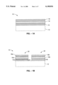
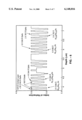
- FIG. 1A is a schematic cross-sectional diagram showing an epitaxial structure in accordance with the present invention.
- FIG. 1B is a schematic cross-sectional diagram showing formation of photodetector and laser cavities from original epitaxial growth in accordance with the present invention.
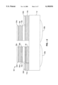
- FIG. 2 is a schematic cross-sectional diagram showing a completed device in accordance with the present invention resulting from the process shown in FIG. 1A and FIG. 1B.
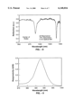
- FIG. 3 is a graph of the vertical refractive index variation in a photodetector and the vertical cavity laser in accordance with the present invention and the relative transverse electric field squared as computed using the transmission matrix technique
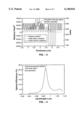
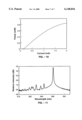
- FIG. 4 is a graph depicting the optical efficiency of a photodetector in accordance with the present invention vs. wavelength.
- FIG. 5 is a graph showing the refractive index vs. depth for an entire structure that was grown by solid source molecular beam epitaxy in accordance with the present invention.
- FIG. 6 is a graph showing the refractive index vs. depth for a region of interest in a structure that was grown by solid source molecular beam epitaxy in accordance with the present invention.
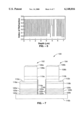
- FIG. 7 is a schematic diagram of an integrated structure fabricated in accordance with the present invention.
- FIG. 8 is a graph showing the reflection spectra of a wafer grown in accordance with the present invention.
- FIG. 9 is a graph showing responsivity vs. wavelength for a photodetector fabricated in accordance with the present invention.
- FIG. 10 is a graph showing optical power and voltage vs. current characteristics for a vertical laser fabricated in accordance with the present invention.
- FIG. 11 is a graph showing the spectra of a vertical laser fabricated in accordance with the present invention.
- the present invention comprises a method for side by side integration of vertical cavity lasers and photodetectors. While the invention is described herein with reference to integration of bottom emitting lasers with bottom illuminated photodetectors, it is also applicable to integration of top emitting lasers with top illuminated photodetectors, top emitting lasers with bottom illuminated photodetectors, and bottom emitting lasers with top illuminated photodetectors.
- the present invention eliminates the need for such a complicated method by processing both devices together on the same substrate with a single epitaxial cavity growth.
- an epitaxial structure 10 comprising a substrate 12, a multilayered bottom DBR 14, a cavity 16 with an emission/absorption medium, and a multilayered top DBR 18, is fabricated in a conventional manner for fabricating vertical cavity devices.
- the bottom DBR 14 is formed as a relatively low index contrast, high refractive index semiconducting material.
- the mirror/cavity/mirror layers in the epitaxial structure 10 shown in FIG. 1A are then separated, preferably by etching, into segments defining a VCSEL region 20 and a photodetector region 22 using conventional techniques such as wet chemical etching or reactive ion etching in conjunction with photolithography.
- substrate 12 now carries adjacent structures which, in combination, will ultimately become a device having an integrated VCSEL and photodetector.
- VCSEL region comprises a bottom mirror segment 14a, a cavity segment 16a, and a top mirror segment 18a.
- Photodetector region 22 is similarly configured.
- a portion 24 of the layers forming bottom DBR segment 14a in VCSEL region 20 are laterally etched or oxidized to achieve a lower refractive index, thus converting the DBR into the high index contrast, high reflectivity DBR necessary for the vertical cavity laser.
- the layers of the bottom DBR 14b in the adjacent photodetector region 22 of the structure are left as grown so that their reflectivity remains low as required for the resonant cavity photodetector.
- FIG. 2 shows a typical complete laser/photodetector device 50 fabricated according to the invention. This is essentially the structure shown in FIG. 1B, except that the laser and photodetector have been further processed for actual use. For example, metal contacts 52a, 52b have been added to the laser and metal contacts 54a, 54b have been added to the photodetector. Note also, the addition of air/oxide apertures 56a, 56b which are commonly used in conventional VCSELs for current/optical confinement. Such fabrication steps may be done before or in conjunction with the previously described steps to define the laser and photodetector regions.
- the top metal electrical contacts may be deposited before the etching to separate the photodetector and the laser or the lateral oxidation of the layers in the bottom DBR may coincide with the formation of the oxide aperture.
- optional integrated microlenses 58a, 58b on the substrate that can be used for collimating and/or focusing the laser beams.
- the resonant wavelength not only of the vertical cavity laser but also of the photodetector.
- Lateral oxidization of high aluminum content AlGaAs will convert it from a refractive index around 3.0 to an oxide with an index ⁇ 1.6, and such a technique has been used to make semiconductor/oxide DBR mirrors in a VCSEL [3].
- Such a large change of index not only alters the reflectivity of the mirror, but also the phase, and so the resonant wavelength of the photodetector may be far from the resonant wavelength of the laser.
- a large change would not be desirable since wavelengths of the peak gain and the peak absorption are not far apart.
- the peaks may be separated by less than a nanometer.
- FIG. 3 shows a graph of the vertical refractive index variation in the photodetector and the vertical cavity laser and the relative transverse electric field squared as computed using the transmission matrix technique.
- FIG. 3 shows only the first portion of the top DBR mirror. The remaining top periods have the same index variation as the first few.
- the exact index and thicknesses of the layers used are given in Table 1.
- Some parasitic absorption is assumed for the doped mirror layers.
- the four mirror periods containing layers which are converted to low index to make the laser consist of ⁇ /8 low index and a 3 ⁇ /8 high index layer.
- the thicker layer above the oxidized mirror periods is a 5 ⁇ /4 layer of GaAs intended as an intracavity contact layer (since the oxide will not conduct current).
- the resonant wavelength for the photodetector is at 986.4 nm and the resonant wavelength for the laser is at 986.3 nm.
- the bottom mirror Before, oxidation the bottom mirror has a transmission of 50% and, after oxidation, the transmission is reduced to 0.67%.
- the material gain in the 8 nm thick quantum wells required for lasing is 1024 cm -1 which is comparable to other working VCSELs.
- the optical efficiency of the photodetector is plotted vs. wavelength in FIG. 4.
- the photodetector has a bandwidth of ⁇ 12 nm, which is sufficiently broad to accommodate variations in the lasers wavelength.
- the optical efficiency of the photodetector is 27%.
- FIG. 5 and FIG. 6 show plots of the refractive index versus depth in a structure that was grown by solid source molecular beam epitaxy. This structure included three layers that were to be oxidized for the VCLs, but not for the photodetectors. Originally the three layers were Al 0 .98 Ga 0 .02 As having a refractive index of 2.98. After oxidation, the index of these layers was reduced to ⁇ 1.55, increasing the reflectivity of the DBR mirror and allowing the device to lase.
- FIG. 7 shows a schematic representation of an integrated structure 100 that was fabricated to provide a VCSEL 102 and a vertical resonant cavity photodetector 104.
- the structure includes p-contacts 106a, 106b, top DBR's 108a, 108b, cavities 110a, 100b with quantum wells, n-contacts 112a, 112b, and bottom DBR's 114a, 114b, all of which are supported by a Si GaAs substrate base 116.
- n+GaAs contact layers 118a, 118b for the bottom DBR's 114a, 114b respectively.
- each of the cavities 110a, 110b comprises three InGaAs quantum wells.
- quantum wells serve to emit light (in the laser) and collect light (in the photodetector) as commonly incorporated in vertical cavity lasers and resonant cavity photodetectors which are not integrated.
- Layers above the quantum wells are p-doped and layers below the quantum wells are n-doped as is common in vertical cavity lasers and resonant cavity photodetectors which are not integrated.
- the oxidized 120a and unoxidized 120b Al 0 .98 Ga 0 .02 As layers that distinguish the bottom DBR 114a for the laser 102 from the bottom DBR 114b for the photodetector 104, as well as intermediate GaAs layers 122a, 122b.
- the first step in processing was the deposition of the p-contacts 106a, 106b.
- mesas around the p-contacts were formed using conventional reactive ion etching. The etching was stopped at the n+GaAs layers 118a, 118b as shown in FIG. 7.
- the n-contacts 112a, 112b were then deposited.
- the p-contact, the mesa on which its sits, and n-contacts were protected with photoresist during an etch in order to expose the layers of Al 0 .98 Ga 0 .02 As, thus creating the double mesa structures shown in FIG. 7.
- SiN was then deposited around the layers 120b of Al 0 .98 Ga 0 .02 As in the photodetector in order to protect them from the lateral oxidation that followed. Preferably, such protection could be avoided by making the lower mesa of the photodetector much larger in order that the lateral oxidation does not extend underneath the photodetector.
- the layers 120a of Al 0 .98 Ga 0 .02 As layers under the vertical cavity laser were then oxidized in a manner similar to that described in [3] in order to create the high reflectivity mirror necessary for lasing.
- FIG. 8 and FIG. 9 show the results from photodetector characterization.
- the reflection spectra of the wafer as grown is shown. This spectra is close to what was predicted by modeling.
- FIG. 9 shows the photodetector's responsivity versus wavelength, which is also close to what was predicted. Such responsivity is too high to come from a reversed biased vertical cavity laser, thus demonstrating the benefits of this novel integration scheme.
- FIG. 10 and FIG. 11 show the results from the vertical cavity laser (VCL) characterization.
- FIG. 10 shows the laser's optical power versus current characteristics.
- FIG. 11 shows the laser's spectra, which is single-mode due to the small size of the device. The narrow peak in the laser's spectra and the high current to light efficiency indicate that lasing is occurring. Note the lasing wavelength is within a nanometer of the peak response of the photodetector.
- the top mirror need not be semiconducting material
- the active region may use other materials, or the exact grading and doping may be different.
- These variations are already common among vertical cavity laser designs in the literature. Therefore, although the description above contains many specificities, these should not be construed as limiting the scope of the invention but as merely providing illustrations of some of the presently preferred embodiments of this invention. Thus the scope of this invention should be determined by the appended claims and their legal equivalents.
Landscapes
- Physics & Mathematics (AREA)
- Condensed Matter Physics & Semiconductors (AREA)
- General Physics & Mathematics (AREA)
- Electromagnetism (AREA)
- Optics & Photonics (AREA)
- Engineering & Computer Science (AREA)
- Computer Hardware Design (AREA)
- Microelectronics & Electronic Packaging (AREA)
- Power Engineering (AREA)
- Semiconductor Lasers (AREA)
Abstract
Description
              TABLE 1
______________________________________
Layer   Thickness
                 n         k
______________________________________
Incident         0.1740        5.6900
 1      455.6    3.518     4.333e - 04
 2      636.0    3.518     8.666e - 05
 3      45.0     3.389     8.666e - 05
 4      45.0     3.261     8.666e - 05
 5      45.0     3.132     8.666e - 05
Repeated 29 times {
 6      689.2    3.003     8.666e - 05
 7      45.0     3.132     8.666e - 05
 8      45.0     3.261     8.666e - 05
 9      45.0     3.389     8.666e - 05
 10     568.5    3.518     1.733e - 04
 11     45.0     3.389     8.666e - 05
 12     45.0     3.261     8.666e - 05
 13     45.0     3.132     8.666e - 05
238     696.7    3.003     4.333e - 05
239     120.0    3.167     4.333e - 05
240     674.8    3.330     4.333e - 05
241     120.0    2.952     4.333e - 05
242     314.8    3.330     4.333e - 05
243     80.0     3.518     0.000e + 00
244     80.0     3.518     (layer with gain/absorption)
245     80.0     3.518     0.000e + 00
246     80.0     3.518     (layer with gain/absorption)
247     80.0     3.518     0.000e + 00
248     80.0     3.518     (layer with gain/absorption)
249     100.0    3.518     0.000e + 00
250     1119.5           3.330       3.939e - 05
251     100.0    3.261     3.939e - 05
252     694.2    3.003     3.939e - 05
253     53.3     3.132     1.970e - 04
254     53.3     3.261     1.970e - 04
255     53.3     3.389     1.970e - 04
Incident
repeated 2 times {
256     543.5    3.518     3.939e - 05
257     53.3     3.389     1.970e - 04
258     53.3     3.261     1.970e - 04
259     53.3     3.132     1.970e - 04
260     664.2    3.003     3.939e - 05
261     53.3     3.132     1.970e - 04
262     53.3     3.261     1.970e - 04
263     53.3     3.389     1.970e - 04
}
272     3437.5           3.518       7.878e - 05
Repeated 4 times {
273     798.4    1.550     0.000e + 00
                           (Layer with low index after
                           oxidation/etching)
274     1055.2           3.518       0.000e + 00
}
Repeated 2 times {
281     838.3    2.952     0.000e + 00
282     703.5    3.518     0.000e + 00
}
285     838.3    2.952     0.000e + 00
Exit              3.5182   0.0000e + 00
______________________________________
 Overall thickness 6.79381 um
Claims (21)
Priority Applications (1)
| Application Number | Priority Date | Filing Date | Title |
|---|---|---|---|
| US09/188,154 US6148016A (en) | 1997-11-06 | 1998-11-05 | Integrated semiconductor lasers and photodetectors |
Applications Claiming Priority (2)
| Application Number | Priority Date | Filing Date | Title |
|---|---|---|---|
| US6472597P | 1997-11-06 | 1997-11-06 | |
| US09/188,154 US6148016A (en) | 1997-11-06 | 1998-11-05 | Integrated semiconductor lasers and photodetectors |
Publications (1)
| Publication Number | Publication Date |
|---|---|
| US6148016A true US6148016A (en) | 2000-11-14 |
Family
ID=26744827
Family Applications (1)
| Application Number | Title | Priority Date | Filing Date |
|---|---|---|---|
| US09/188,154 Expired - Fee Related US6148016A (en) | 1997-11-06 | 1998-11-05 | Integrated semiconductor lasers and photodetectors |
Country Status (1)
| Country | Link |
|---|---|
| US (1) | US6148016A (en) |
Cited By (52)
| Publication number | Priority date | Publication date | Assignee | Title |
|---|---|---|---|---|
| US20010019566A1 (en) * | 1995-12-18 | 2001-09-06 | Jack Jewell | Conductive element with lateral oxidation barrier |
| WO2002047128A1 (en) * | 2000-12-06 | 2002-06-13 | Applied Optoelectronics, Inc. | Patterned phase shift layers for wavelength-selectable vertical-cavity surface-emitting laser (vcsel) arrays |
| US6455340B1 (en) | 2001-12-21 | 2002-09-24 | Xerox Corporation | Method of fabricating GaN semiconductor structures using laser-assisted epitaxial liftoff |
| US6495381B2 (en) * | 2000-05-18 | 2002-12-17 | Samsung Electronics Co., Ltd. | Apparatus and method for forming aperture of vertical cavity surface emitting laser by selective oxidation |
| US20030067009A1 (en) * | 1999-12-27 | 2003-04-10 | Xerox Corporation | Structure and method for electrical isolation of optoelectronic integrated circuits |
| US6636544B2 (en) | 2000-12-06 | 2003-10-21 | Applied Optoelectronics, Inc. | Overlapping wavelength-tunable vertical cavity surface-emitting laser (VCSEL) arrays |
| US6683326B2 (en) * | 2000-11-14 | 2004-01-27 | Sumitomo Electric Industries, Ltd. | Semiconductor photodiode and an optical receiver |
| WO2004015783A1 (en) * | 2002-08-13 | 2004-02-19 | The University Of Western Australia | A resonant cavity enhanced device and a method for fabricating same |
| US6696307B2 (en) | 2000-12-06 | 2004-02-24 | Applied Optoelectronics, Inc. | Patterned phase shift layers for wavelength-selectable vertical cavity surface-emitting laser (VCSEL) arrays |
| US6724796B2 (en) | 2000-12-06 | 2004-04-20 | Applied Optoelectronics, Inc. | Modified distributed bragg reflector (DBR) for vertical cavity surface-emitting laser (VCSEL) resonant wavelength tuning sensitivity control |
| US6815656B1 (en) | 2001-03-01 | 2004-11-09 | Lauer Mark A | Integrated optical cross-connect amplifier |
| US6822995B2 (en) | 2002-02-21 | 2004-11-23 | Finisar Corporation | GaAs/AI(Ga)As distributed bragg reflector on InP |
| US20050019973A1 (en) * | 2003-07-23 | 2005-01-27 | Palo Alto Research Center, Incorporated | Phase array oxide-confined VCSEL |
| US20050110026A1 (en) * | 2003-09-30 | 2005-05-26 | Osram Opto Semiconductors Gmbh | Radiation-emitting-and-receiving semiconductor chip and method for producing such a semiconductor chip |
| US20050117853A1 (en) * | 2000-12-28 | 2005-06-02 | Venkatesan Murali | Optical subassembly |
| US20050123015A1 (en) * | 1998-12-21 | 2005-06-09 | Johnson Ralph H. | Use of GaAs extended barrier layers between active regions containing nitrogen and AlGaAs confining layers |
| US20050129078A1 (en) * | 1998-12-21 | 2005-06-16 | Johnson Ralph H. | Multicomponent barrier layers in quantum well active regions to enhance confinement and speed |
| US20050158902A1 (en) * | 1997-02-07 | 2005-07-21 | Xerox Corporation | Method and structure for eliminating polarization instability in laterally - oxidized VCSELs |
| US6922426B2 (en) | 2001-12-20 | 2005-07-26 | Finisar Corporation | Vertical cavity surface emitting laser including indium in the active region |
| US20050243327A1 (en) * | 2003-02-14 | 2005-11-03 | Chian Chiu Li | Compact Optical Apparatus |
| US6967981B2 (en) | 2002-05-30 | 2005-11-22 | Xerox Corporation | Nitride based semiconductor structures with highly reflective mirrors |
| US6975660B2 (en) | 2001-12-27 | 2005-12-13 | Finisar Corporation | Vertical cavity surface emitting laser including indium and antimony in the active region |
| US20060060755A1 (en) * | 2004-09-18 | 2006-03-23 | Chian Chiu Li | Bi-directional Optical Transmission System And Method |
| US7058112B2 (en) | 2001-12-27 | 2006-06-06 | Finisar Corporation | Indium free vertical cavity surface emitting laser |
| US7095770B2 (en) | 2001-12-20 | 2006-08-22 | Finisar Corporation | Vertical cavity surface emitting laser including indium, antimony and nitrogen in the active region |
| US20060246700A1 (en) * | 1998-12-21 | 2006-11-02 | Johnson Ralph H | Migration enhanced epitaxy fabrication of active regions having quantum wells |
| US20060276002A1 (en) * | 2005-05-12 | 2006-12-07 | Sheila Tandon | Integration of buried oxide layers with crystalline layers |
| US20070003288A1 (en) * | 2005-06-30 | 2007-01-04 | Xiaolin Tong | Bidirectional HDCP transmission module using single optical fiber |
| US20070096150A1 (en) * | 2005-11-01 | 2007-05-03 | Matsushita Electric Industrial Co., Ltd. | Heterojunction bipolar transistor |
| US20070242062A1 (en) * | 2006-04-18 | 2007-10-18 | Yong Guo | EDID pass through via serial channel |
| US7286585B2 (en) | 1998-12-21 | 2007-10-23 | Finisar Corporation | Low temperature grown layers with migration enhanced epitaxy adjacent to an InGaAsN(Sb) based active region |
| US7295586B2 (en) | 2002-02-21 | 2007-11-13 | Finisar Corporation | Carbon doped GaAsSb suitable for use in tunnel junctions of long-wavelength VCSELs |
| US20070280282A1 (en) * | 2006-06-05 | 2007-12-06 | Tzeng Shing-Wu P | Indoor digital multimedia networking |
| US20070286600A1 (en) * | 2006-06-09 | 2007-12-13 | Owlink Technology, Inc. | Universal IR Repeating over Optical Fiber |
| US20070292135A1 (en) * | 2006-06-09 | 2007-12-20 | Yong Guo | Integrated remote control signaling |
| US7378680B2 (en) | 1998-12-21 | 2008-05-27 | Finisar Corporation | Migration enhanced epitaxy fabrication of quantum wells |
| US7408964B2 (en) | 2001-12-20 | 2008-08-05 | Finisar Corporation | Vertical cavity surface emitting laser including indium and nitrogen in the active region |
| US7412170B1 (en) | 2003-05-29 | 2008-08-12 | Opticomp Corporation | Broad temperature WDM transmitters and receivers for coarse wavelength division multiplexed (CWDM) fiber communication systems |
| US20080291074A1 (en) * | 2007-05-22 | 2008-11-27 | Owlink Technology, Inc. | Universal Remote Control Device |
| US20100014806A1 (en) * | 2006-09-13 | 2010-01-21 | Edith Cowan University | Optical connection component |
| WO2010088728A1 (en) * | 2009-02-05 | 2010-08-12 | Edith Cowan University | An optical connection system |
| US8168456B2 (en) | 2004-10-01 | 2012-05-01 | Finisar Corporation | Vertical cavity surface emitting laser with undoped top mirror |
| US8451875B2 (en) | 2004-10-01 | 2013-05-28 | Finisar Corporation | Vertical cavity surface emitting laser having strain reduced quantum wells |
| US8638832B2 (en) | 2010-10-04 | 2014-01-28 | Furakawa Electric Co., Ltd. | Electronic device, surface emitting laser, surface emitting laser array, light source, optical module |
| JP2017117891A (en) * | 2015-12-22 | 2017-06-29 | 株式会社リコー | Optical sensor, optical inspection apparatus, and optical characteristics detection method |
| CN106936068A (en) * | 2015-12-30 | 2017-07-07 | 中国科学院苏州纳米技术与纳米仿生研究所 | A kind of integration laser and preparation method thereof |
| JP2018046314A (en) * | 2013-10-30 | 2018-03-22 | 京セラ株式会社 | Light receiving/emitting element and sensor device using the same |
| JP2018074075A (en) * | 2016-11-02 | 2018-05-10 | 株式会社リコー | Light irradiator, optical sensor, and optical inspection device |
| US20190140424A1 (en) * | 2016-08-29 | 2019-05-09 | International Business Machines Corporation | Resonant Cavity Strained Group III-V Photodetector And LED On Silicon Substrate And Method To Fabricate Same |
| CN110178044A (en) * | 2017-01-23 | 2019-08-27 | 深圳源光科技有限公司 | Laser radar |
| JP2020092256A (en) * | 2018-11-27 | 2020-06-11 | 株式会社リコー | Light source, light source device, optical device, measuring device, robot, electronic apparatus, movable body, and molding device |
| CN111711068A (en) * | 2020-05-06 | 2020-09-25 | 浙江博升光电科技有限公司 | Optical chip |
Citations (12)
| Publication number | Priority date | Publication date | Assignee | Title |
|---|---|---|---|---|
| US5491712A (en) * | 1994-10-31 | 1996-02-13 | Lin; Hong | Integration of surface emitting laser and photodiode for monitoring power output of surface emitting laser |
| US5513204A (en) * | 1995-04-12 | 1996-04-30 | Optical Concepts, Inc. | Long wavelength, vertical cavity surface emitting laser with vertically integrated optical pump |
| US5748661A (en) * | 1996-07-19 | 1998-05-05 | Motorola, Inc. | Integrated lateral detector and laser device and method of fabrication |
| US5751757A (en) * | 1996-07-01 | 1998-05-12 | Motorola, Inc. | VCSEL with integrated MSM photodetector |
| US5757837A (en) * | 1996-10-16 | 1998-05-26 | The Regents Of The University Of California | Intracavity quantum well photodetector integrated within a vertical-cavity surface-emitting laser and method of operating same |
| US5757836A (en) * | 1996-07-01 | 1998-05-26 | Motorola, Inc. | Vertical cavity surface emitting laser with laterally integrated photodetector |
| US5801402A (en) * | 1996-01-23 | 1998-09-01 | Samsung Electronics Co., Ltd. | VCSEL light output apparatus having a monitoring photodetector and an optical pickup apparatus employing the same |
| US5835521A (en) * | 1997-02-10 | 1998-11-10 | Motorola, Inc. | Long wavelength light emitting vertical cavity surface emitting laser and method of fabrication |
| US5864575A (en) * | 1995-12-26 | 1999-01-26 | Nippon Telegraph And Telephone Corporation | Vertical-cavity surface-emitting laser and method for manufacturing the same |
| US5978408A (en) * | 1997-02-07 | 1999-11-02 | Xerox Corporation | Highly compact vertical cavity surface emitting lasers |
| US5978401A (en) * | 1995-10-25 | 1999-11-02 | Honeywell Inc. | Monolithic vertical cavity surface emitting laser and resonant cavity photodetector transceiver |
| US6052398A (en) * | 1997-04-03 | 2000-04-18 | Alcatel | Surface emitting semiconductor laser |
-
1998
- 1998-11-05 US US09/188,154 patent/US6148016A/en not_active Expired - Fee Related
Patent Citations (13)
| Publication number | Priority date | Publication date | Assignee | Title |
|---|---|---|---|---|
| US5491712A (en) * | 1994-10-31 | 1996-02-13 | Lin; Hong | Integration of surface emitting laser and photodiode for monitoring power output of surface emitting laser |
| US5838708A (en) * | 1994-10-31 | 1998-11-17 | Hewlett-Packard Company | Integration of surface emitting laser and photodiode for monitoring power output of surface emitting laser |
| US5513204A (en) * | 1995-04-12 | 1996-04-30 | Optical Concepts, Inc. | Long wavelength, vertical cavity surface emitting laser with vertically integrated optical pump |
| US5978401A (en) * | 1995-10-25 | 1999-11-02 | Honeywell Inc. | Monolithic vertical cavity surface emitting laser and resonant cavity photodetector transceiver |
| US5864575A (en) * | 1995-12-26 | 1999-01-26 | Nippon Telegraph And Telephone Corporation | Vertical-cavity surface-emitting laser and method for manufacturing the same |
| US5801402A (en) * | 1996-01-23 | 1998-09-01 | Samsung Electronics Co., Ltd. | VCSEL light output apparatus having a monitoring photodetector and an optical pickup apparatus employing the same |
| US5757836A (en) * | 1996-07-01 | 1998-05-26 | Motorola, Inc. | Vertical cavity surface emitting laser with laterally integrated photodetector |
| US5751757A (en) * | 1996-07-01 | 1998-05-12 | Motorola, Inc. | VCSEL with integrated MSM photodetector |
| US5748661A (en) * | 1996-07-19 | 1998-05-05 | Motorola, Inc. | Integrated lateral detector and laser device and method of fabrication |
| US5757837A (en) * | 1996-10-16 | 1998-05-26 | The Regents Of The University Of California | Intracavity quantum well photodetector integrated within a vertical-cavity surface-emitting laser and method of operating same |
| US5978408A (en) * | 1997-02-07 | 1999-11-02 | Xerox Corporation | Highly compact vertical cavity surface emitting lasers |
| US5835521A (en) * | 1997-02-10 | 1998-11-10 | Motorola, Inc. | Long wavelength light emitting vertical cavity surface emitting laser and method of fabrication |
| US6052398A (en) * | 1997-04-03 | 2000-04-18 | Alcatel | Surface emitting semiconductor laser |
Cited By (78)
| Publication number | Priority date | Publication date | Assignee | Title |
|---|---|---|---|---|
| US20010019566A1 (en) * | 1995-12-18 | 2001-09-06 | Jack Jewell | Conductive element with lateral oxidation barrier |
| US20020186735A1 (en) * | 1995-12-18 | 2002-12-12 | Jack Jewell | Conductive element with lateral oxidation barrier |
| US7079560B2 (en) | 1995-12-18 | 2006-07-18 | Picolight Incorporated | Light emitting device |
| US6459713B2 (en) * | 1995-12-18 | 2002-10-01 | Picolight Incorporated | Conductive element with lateral oxidation barrier |
| US6765943B2 (en) | 1995-12-18 | 2004-07-20 | Picolight, Incorporated | Light emitting device |
| US20060187991A1 (en) * | 1997-02-07 | 2006-08-24 | Xerox Corporation | Laterally oxidized vertical cavity surface emitting lasers |
| US7160749B2 (en) | 1997-02-07 | 2007-01-09 | Xerox Corporation | Method and structure for eliminating polarization instability in laterally—oxidized VCSELs |
| US7596161B2 (en) | 1997-02-07 | 2009-09-29 | Xerox Corporation | Laterally oxidized vertical cavity surface emitting lasers |
| US20050158902A1 (en) * | 1997-02-07 | 2005-07-21 | Xerox Corporation | Method and structure for eliminating polarization instability in laterally - oxidized VCSELs |
| US7286585B2 (en) | 1998-12-21 | 2007-10-23 | Finisar Corporation | Low temperature grown layers with migration enhanced epitaxy adjacent to an InGaAsN(Sb) based active region |
| US7435660B2 (en) | 1998-12-21 | 2008-10-14 | Finisar Corporation | Migration enhanced epitaxy fabrication of active regions having quantum wells |
| US7378680B2 (en) | 1998-12-21 | 2008-05-27 | Finisar Corporation | Migration enhanced epitaxy fabrication of quantum wells |
| US7257143B2 (en) | 1998-12-21 | 2007-08-14 | Finisar Corporation | Multicomponent barrier layers in quantum well active regions to enhance confinement and speed |
| US20060246700A1 (en) * | 1998-12-21 | 2006-11-02 | Johnson Ralph H | Migration enhanced epitaxy fabrication of active regions having quantum wells |
| US7167495B2 (en) | 1998-12-21 | 2007-01-23 | Finisar Corporation | Use of GaAs extended barrier layers between active regions containing nitrogen and AlGaAs confining layers |
| US20050123015A1 (en) * | 1998-12-21 | 2005-06-09 | Johnson Ralph H. | Use of GaAs extended barrier layers between active regions containing nitrogen and AlGaAs confining layers |
| US20050129078A1 (en) * | 1998-12-21 | 2005-06-16 | Johnson Ralph H. | Multicomponent barrier layers in quantum well active regions to enhance confinement and speed |
| US7195939B2 (en) * | 1999-12-27 | 2007-03-27 | Xerox Corporation | Structure and method for electrical isolation of optoelectronic integrated circuits |
| US20030067009A1 (en) * | 1999-12-27 | 2003-04-10 | Xerox Corporation | Structure and method for electrical isolation of optoelectronic integrated circuits |
| US6495381B2 (en) * | 2000-05-18 | 2002-12-17 | Samsung Electronics Co., Ltd. | Apparatus and method for forming aperture of vertical cavity surface emitting laser by selective oxidation |
| US6683326B2 (en) * | 2000-11-14 | 2004-01-27 | Sumitomo Electric Industries, Ltd. | Semiconductor photodiode and an optical receiver |
| WO2002047128A1 (en) * | 2000-12-06 | 2002-06-13 | Applied Optoelectronics, Inc. | Patterned phase shift layers for wavelength-selectable vertical-cavity surface-emitting laser (vcsel) arrays |
| US6636544B2 (en) | 2000-12-06 | 2003-10-21 | Applied Optoelectronics, Inc. | Overlapping wavelength-tunable vertical cavity surface-emitting laser (VCSEL) arrays |
| US6696307B2 (en) | 2000-12-06 | 2004-02-24 | Applied Optoelectronics, Inc. | Patterned phase shift layers for wavelength-selectable vertical cavity surface-emitting laser (VCSEL) arrays |
| US6724796B2 (en) | 2000-12-06 | 2004-04-20 | Applied Optoelectronics, Inc. | Modified distributed bragg reflector (DBR) for vertical cavity surface-emitting laser (VCSEL) resonant wavelength tuning sensitivity control |
| US20050117853A1 (en) * | 2000-12-28 | 2005-06-02 | Venkatesan Murali | Optical subassembly |
| US7066657B2 (en) | 2000-12-28 | 2006-06-27 | Intel Corporation | Optical subassembly |
| US6815656B1 (en) | 2001-03-01 | 2004-11-09 | Lauer Mark A | Integrated optical cross-connect amplifier |
| US6922426B2 (en) | 2001-12-20 | 2005-07-26 | Finisar Corporation | Vertical cavity surface emitting laser including indium in the active region |
| US7408964B2 (en) | 2001-12-20 | 2008-08-05 | Finisar Corporation | Vertical cavity surface emitting laser including indium and nitrogen in the active region |
| US7095770B2 (en) | 2001-12-20 | 2006-08-22 | Finisar Corporation | Vertical cavity surface emitting laser including indium, antimony and nitrogen in the active region |
| US6455340B1 (en) | 2001-12-21 | 2002-09-24 | Xerox Corporation | Method of fabricating GaN semiconductor structures using laser-assisted epitaxial liftoff |
| US7058112B2 (en) | 2001-12-27 | 2006-06-06 | Finisar Corporation | Indium free vertical cavity surface emitting laser |
| US6975660B2 (en) | 2001-12-27 | 2005-12-13 | Finisar Corporation | Vertical cavity surface emitting laser including indium and antimony in the active region |
| US7295586B2 (en) | 2002-02-21 | 2007-11-13 | Finisar Corporation | Carbon doped GaAsSb suitable for use in tunnel junctions of long-wavelength VCSELs |
| US6822995B2 (en) | 2002-02-21 | 2004-11-23 | Finisar Corporation | GaAs/AI(Ga)As distributed bragg reflector on InP |
| US6967981B2 (en) | 2002-05-30 | 2005-11-22 | Xerox Corporation | Nitride based semiconductor structures with highly reflective mirrors |
| US7541584B2 (en) | 2002-08-13 | 2009-06-02 | The University Of Western Australia | Resonant cavity enhanced device and a method for fabricating same |
| US20060118721A1 (en) * | 2002-08-13 | 2006-06-08 | Jarek Antoszewski | Resonant cavity enhanced device and a method for fabricating same |
| WO2004015783A1 (en) * | 2002-08-13 | 2004-02-19 | The University Of Western Australia | A resonant cavity enhanced device and a method for fabricating same |
| US7280222B2 (en) | 2003-02-14 | 2007-10-09 | Chian Chiu Li | Compact optical apparatus |
| US20050243327A1 (en) * | 2003-02-14 | 2005-11-03 | Chian Chiu Li | Compact Optical Apparatus |
| US7412170B1 (en) | 2003-05-29 | 2008-08-12 | Opticomp Corporation | Broad temperature WDM transmitters and receivers for coarse wavelength division multiplexed (CWDM) fiber communication systems |
| US7257141B2 (en) | 2003-07-23 | 2007-08-14 | Palo Alto Research Center Incorporated | Phase array oxide-confined VCSELs |
| US20050019973A1 (en) * | 2003-07-23 | 2005-01-27 | Palo Alto Research Center, Incorporated | Phase array oxide-confined VCSEL |
| US7524687B2 (en) | 2003-09-30 | 2009-04-28 | Osram Opto Semiconductors Gmbh | Method for producing a radiation-emitting-and-receiving semiconductor chip |
| US7335922B2 (en) | 2003-09-30 | 2008-02-26 | Osram Opto Semiconductors Gmbh | Radiation-emitting-and-receiving semiconductor chip and method for producing such a semiconductor chip |
| US20050110026A1 (en) * | 2003-09-30 | 2005-05-26 | Osram Opto Semiconductors Gmbh | Radiation-emitting-and-receiving semiconductor chip and method for producing such a semiconductor chip |
| US20080153189A1 (en) * | 2003-09-30 | 2008-06-26 | Osram Opto Semiconductors Gmbh | Method for producing a radiation-emitting-and-receiving semiconductor chip |
| EP1536479A1 (en) * | 2003-09-30 | 2005-06-01 | Osram Opto Semiconductors GmbH | Light-emitting and -receiving semiconductor device and its manufacturing process |
| US20060060755A1 (en) * | 2004-09-18 | 2006-03-23 | Chian Chiu Li | Bi-directional Optical Transmission System And Method |
| US7385175B2 (en) | 2004-09-18 | 2008-06-10 | Chian Chiu Li | Bi-directional optical transmission system and method |
| US8168456B2 (en) | 2004-10-01 | 2012-05-01 | Finisar Corporation | Vertical cavity surface emitting laser with undoped top mirror |
| US8451875B2 (en) | 2004-10-01 | 2013-05-28 | Finisar Corporation | Vertical cavity surface emitting laser having strain reduced quantum wells |
| US8008215B2 (en) * | 2005-05-12 | 2011-08-30 | Massachusetts Institute Of Technology | Integration of buried oxide layers with crystalline layers |
| US20060276002A1 (en) * | 2005-05-12 | 2006-12-07 | Sheila Tandon | Integration of buried oxide layers with crystalline layers |
| US20070003288A1 (en) * | 2005-06-30 | 2007-01-04 | Xiaolin Tong | Bidirectional HDCP transmission module using single optical fiber |
| US20070096150A1 (en) * | 2005-11-01 | 2007-05-03 | Matsushita Electric Industrial Co., Ltd. | Heterojunction bipolar transistor |
| US20070242062A1 (en) * | 2006-04-18 | 2007-10-18 | Yong Guo | EDID pass through via serial channel |
| US20070280282A1 (en) * | 2006-06-05 | 2007-12-06 | Tzeng Shing-Wu P | Indoor digital multimedia networking |
| US20070286600A1 (en) * | 2006-06-09 | 2007-12-13 | Owlink Technology, Inc. | Universal IR Repeating over Optical Fiber |
| US20070292135A1 (en) * | 2006-06-09 | 2007-12-20 | Yong Guo | Integrated remote control signaling |
| US8197147B2 (en) | 2006-09-13 | 2012-06-12 | Edith Cowan University | Optical connection component |
| US20100014806A1 (en) * | 2006-09-13 | 2010-01-21 | Edith Cowan University | Optical connection component |
| US20080291074A1 (en) * | 2007-05-22 | 2008-11-27 | Owlink Technology, Inc. | Universal Remote Control Device |
| US8150261B2 (en) | 2007-05-22 | 2012-04-03 | Owlink Technology, Inc. | Universal remote control device |
| WO2010088728A1 (en) * | 2009-02-05 | 2010-08-12 | Edith Cowan University | An optical connection system |
| US8638832B2 (en) | 2010-10-04 | 2014-01-28 | Furakawa Electric Co., Ltd. | Electronic device, surface emitting laser, surface emitting laser array, light source, optical module |
| DE112011102431B4 (en) * | 2010-10-04 | 2014-03-06 | Furukawa Electric Co., Ltd., | Electronic device, surface emitting laser, surface emitting laser array, light source, optical module |
| JP2018046314A (en) * | 2013-10-30 | 2018-03-22 | 京セラ株式会社 | Light receiving/emitting element and sensor device using the same |
| JP2017117891A (en) * | 2015-12-22 | 2017-06-29 | 株式会社リコー | Optical sensor, optical inspection apparatus, and optical characteristics detection method |
| CN106936068A (en) * | 2015-12-30 | 2017-07-07 | 中国科学院苏州纳米技术与纳米仿生研究所 | A kind of integration laser and preparation method thereof |
| US20190140424A1 (en) * | 2016-08-29 | 2019-05-09 | International Business Machines Corporation | Resonant Cavity Strained Group III-V Photodetector And LED On Silicon Substrate And Method To Fabricate Same |
| US10601199B2 (en) * | 2016-08-29 | 2020-03-24 | International Business Machines Corporation | Resonant cavity strained group III-V photodetector and LED on silicon substrate and method to fabricate same |
| JP2018074075A (en) * | 2016-11-02 | 2018-05-10 | 株式会社リコー | Light irradiator, optical sensor, and optical inspection device |
| CN110178044A (en) * | 2017-01-23 | 2019-08-27 | 深圳源光科技有限公司 | Laser radar |
| JP2020092256A (en) * | 2018-11-27 | 2020-06-11 | 株式会社リコー | Light source, light source device, optical device, measuring device, robot, electronic apparatus, movable body, and molding device |
| CN111711068A (en) * | 2020-05-06 | 2020-09-25 | 浙江博升光电科技有限公司 | Optical chip |
Similar Documents
| Publication | Publication Date | Title |
|---|---|---|
| US6148016A (en) | Integrated semiconductor lasers and photodetectors | |
| US7288421B2 (en) | Method for forming an optoelectronic device having an isolation layer | |
| US6836501B2 (en) | Resonant reflector for increased wavelength and polarization control | |
| US5978401A (en) | Monolithic vertical cavity surface emitting laser and resonant cavity photodetector transceiver | |
| EP1309051B1 (en) | Optical data path comprising a vertical cavity surface emitting laser VCSEL and a resonant cavity photo-diode RCPD | |
| EP1955855B1 (en) | Surface light emitting laser element, surface light emitting laser array provided with it, electro-photographic system and optical communication system | |
| US7787511B2 (en) | Array of surface-emitting laser diodes having reduced device resistance and capable of performing high output operation and method of fabricating the surface-emitting laser diode | |
| EP1352455B1 (en) | Spatially modulated reflector for an optoelectronic device | |
| US5732103A (en) | Long wavelength VCSEL | |
| US20020163688A1 (en) | Optical communications system and vertical cavity surface emitting laser therefor | |
| EP0565374B1 (en) | Vertical-to-surface transmission electrophotonic device | |
| US8599897B2 (en) | Tunable detector | |
| US7154927B2 (en) | Surface emitting semiconductor laser and communication system using the same | |
| US6084900A (en) | Annular waveguide vertical cavity surface emitting laser array and method of fabrication | |
| US5956364A (en) | Vertical cavity surface emitting laser with shaped cavity mirror and method of fabrication | |
| JPH09199793A (en) | Vertical cavity surface emitting lasers | |
| US6061485A (en) | Method for wavelength division multiplexing utilizing donut mode vertical cavity surface emitting lasers | |
| US20020159491A1 (en) | Surface emitting laser | |
| US7277461B2 (en) | Dielectric VCSEL gain guide | |
| Yang et al. | Monolithic oxide-confined multiple-wavelength vertical-cavity surface-emitting laser arrays with a 57-nm wavelength grading range using an oxidized upper Bragg mirror |
Legal Events
| Date | Code | Title | Description |
|---|---|---|---|
| AS | Assignment |
Owner name: REGENTS OF THE UNIVERSITY OF CALIFORNIA, THE, CALI Free format text: ASSIGNMENT OF ASSIGNORS INTEREST;ASSIGNORS:HEGBLOM, ERIC R.;LOUDERBACK, DUANE A.;REEL/FRAME:009746/0198 Effective date: 19980120 |
|
| FEPP | Fee payment procedure |
Free format text: PAYOR NUMBER ASSIGNED (ORIGINAL EVENT CODE: ASPN); ENTITY STATUS OF PATENT OWNER: SMALL ENTITY |
|
| FPAY | Fee payment |
Year of fee payment: 4 |
|
| FPAY | Fee payment |
Year of fee payment: 8 |
|
| AS | Assignment |
Owner name: UNITED STATES AIR FORCE,VIRGINIA Free format text: CONFIRMATORY LICENSE;ASSIGNOR:UNIVERSITY OF CALIFORNIA;REEL/FRAME:024413/0922 Effective date: 20080724 |
|
| AS | Assignment |
Owner name: UNITED STATES, AIR FORCE, VIRGINIA Free format text: CONFIRMATORY LICENSE;ASSIGNOR:UNIVERSITY OF CALIFORNIA;REEL/FRAME:025309/0027 Effective date: 20080724 |
|
| REMI | Maintenance fee reminder mailed | ||
| LAPS | Lapse for failure to pay maintenance fees | ||
| STCH | Information on status: patent discontinuation |
Free format text: PATENT EXPIRED DUE TO NONPAYMENT OF MAINTENANCE FEES UNDER 37 CFR 1.362 |
|
| FP | Lapsed due to failure to pay maintenance fee |
Effective date: 20121114 |