US6147953A - Optical signal transmission apparatus - Google Patents
Optical signal transmission apparatus Download PDFInfo
- Publication number
- US6147953A US6147953A US09/048,169 US4816998A US6147953A US 6147953 A US6147953 A US 6147953A US 4816998 A US4816998 A US 4816998A US 6147953 A US6147953 A US 6147953A
- Authority
- US
- United States
- Prior art keywords
- optical
- optical signal
- signal transmission
- optical coupler
- light
- Prior art date
- Legal status (The legal status is an assumption and is not a legal conclusion. Google has not performed a legal analysis and makes no representation as to the accuracy of the status listed.)
- Expired - Fee Related
Links
Images

Classifications
-
- G—PHYSICS
- G11—INFORMATION STORAGE
- G11B—INFORMATION STORAGE BASED ON RELATIVE MOVEMENT BETWEEN RECORD CARRIER AND TRANSDUCER
- G11B7/00—Recording or reproducing by optical means, e.g. recording using a thermal beam of optical radiation by modifying optical properties or the physical structure, reproducing using an optical beam at lower power by sensing optical properties; Record carriers therefor
- G11B7/12—Heads, e.g. forming of the optical beam spot or modulation of the optical beam
- G11B7/135—Means for guiding the beam from the source to the record carrier or from the record carrier to the detector
- G11B7/1384—Fibre optics
-
- G—PHYSICS
- G02—OPTICS
- G02B—OPTICAL ELEMENTS, SYSTEMS OR APPARATUS
- G02B6/00—Light guides; Structural details of arrangements comprising light guides and other optical elements, e.g. couplings
- G02B6/24—Coupling light guides
- G02B6/42—Coupling light guides with opto-electronic elements
- G02B6/4201—Packages, e.g. shape, construction, internal or external details
- G02B6/4246—Bidirectionally operating package structures
-
- G—PHYSICS
- G11—INFORMATION STORAGE
- G11B—INFORMATION STORAGE BASED ON RELATIVE MOVEMENT BETWEEN RECORD CARRIER AND TRANSDUCER
- G11B7/00—Recording or reproducing by optical means, e.g. recording using a thermal beam of optical radiation by modifying optical properties or the physical structure, reproducing using an optical beam at lower power by sensing optical properties; Record carriers therefor
- G11B7/12—Heads, e.g. forming of the optical beam spot or modulation of the optical beam
- G11B7/135—Means for guiding the beam from the source to the record carrier or from the record carrier to the detector
- G11B7/1359—Single prisms
-
- G—PHYSICS
- G11—INFORMATION STORAGE
- G11B—INFORMATION STORAGE BASED ON RELATIVE MOVEMENT BETWEEN RECORD CARRIER AND TRANSDUCER
- G11B7/00—Recording or reproducing by optical means, e.g. recording using a thermal beam of optical radiation by modifying optical properties or the physical structure, reproducing using an optical beam at lower power by sensing optical properties; Record carriers therefor
- G11B7/12—Heads, e.g. forming of the optical beam spot or modulation of the optical beam
- G11B7/135—Means for guiding the beam from the source to the record carrier or from the record carrier to the detector
- G11B7/1372—Lenses
Definitions
- This invention relates to optical signal transmission apparatus and more particularly to an integrated optical coupler employed in association with one or more laser diodes or light emitting diodes (LEDs).
- the coupler allows separation and detection of a return optical signal or may be employed for other purposes such as efficient combining of output from a plurality of diode lasers.
- diode lasers and LEDs involve the columnation of or focusing of the emitted optical signal and measurement of a return signal along the optical axis of the outgoing signal.
- Examples of such systems include magneto-optical, CD-ROM, and DVD computer mass storage devices wherein a diode laser is focused onto a spot on the recording media and a reflected signal is measured.
- Prior art optics for such systems conventionally include a plurality of separate optical elements through which the laser light must pass. It is not untypical for the laser light to pass through eight or more separate optical surfaces prior to arriving at the storage media and six or more additional surfaces before arriving at a photodetector. Significant optical losses and degradation of signal quality occur due to optical signal passage through these surfaces. Alignment of the laser and the optical elements employed is critical and misalignment can and does occur on an all too frequent basis.
- the optical couplers employed cause significant loss of optical signal, often resulting in a small percentage of the emitter energy arriving at the photodetector employed in such systems. This is true regardless of the type of emitter-to-fiber couplers employed in prior arrangements, including for example, cylindrical lenses, butt contact, spherical ball couplers, and aspheric lenses.
- the present invention relates to optical signal transmission apparatus which utilizes an optical coupler of specialized character which is simple and relatively inexpensive and is highly reliable and efficient in operation in a variety of optical signal transmission environments.
- the invention includes a first optical coupler element formed of light transmitting material for receiving an optical signal and transmitting the optical signal in a linear direction and having at least one convex surface and a planar surface, the planar surface being disposed at an angle to the linear direction.
- a second optical coupler element formed of light transmitting material having a planar surface is bonded along a planar junction to the planar surface of the first optical coupler element.
- At least one coating is disposed at the planar junction for reflecting and redirecting at least a portion of an optical signal transmitted by the first optical coupler element to a surface of the optical signal transmission apparatus.
- the planar junction disclosed herein is disposed at a generally forty-five degree angle relative to the linear direction of optical signal transmission.
- the optical coupler is employed in conjunction with one or more photodetectors to sense the redirected optical signal.
- Another embodiment of the invention utilizes the optical coupler to combine the optical signal from two diode lasers into a single optical signal and either couple the signal into an optical fiber by focusing the light to a spot or emit the combined signal as a collimated beam using a single optical element.
- the unitary optical coupler performs the functions of collimating a diode laser, rotation of the diode laser beam polarization, focusing of the outgoing beam, and collimation and separation of a returning beam to be perpendicular to the diode laser axis.
- the invention is utilized to provide spectral separation of the return light, allowing multi-channel radiometer detection using photodetectors or spectrometer detection using a series of photodetectors.
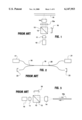
- FIG. 1 is a schematic view illustrating conventional prior art pick-up optics used in an optical storage system for computers
- FIG. 2 is a schematic view showing a typical known duplex fiber optic communication system
- FIG. 3 is a schematic view illustrating a prior art fiber optic sensor
- FIG. 4 is a schematic view of one form of optical coupler constructed in accordance with the teachings of the present invention receiving polarized light from a diode laser, reflecting the laser beam from an internal coated surface and transmitting the returning optical signal to an optical sensor;
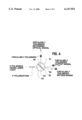
- FIG. 5 illustrates an alternative embodiment of the optical coupler wherein a diode laser beam is transmitted through the internal coated surface thereof and the returning optical signal is reflected to an optical sensor;
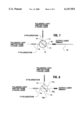
- FIG. 6 illustrates yet another embodiment of the optical coupler wherein a diode laser beam is transmitted through the internal coated surface thereof, circularly polarized using a quarter wave retardation plate, and focused into a spot upon exiting the optical coupler;
- FIG. 7 illustrates the optical coupler disclosed in FIG. 5 to combine and couple diode laser output beams for input into an optical fiber
- FIG. 8 illustrates an alternate embodiment of the optical coupler receiving laser light from two diode lasers and combining and converting same into a collimated beam
- FIG. 9 illustrates yet another embodiment of the optical coupler employed in combination with a diffraction grating to provide wavelength separation of a returning signal
- FIG. 10 is a schematic illustration illustrating application of the optical coupler for duplex fiberoptic communications
- FIG. 11 is a schematic presentation illustrating application of an optical coupler constructed in accordance with the teachings of the present invention for optical sensing
- FIG. 12 illustrates the invention being employed as pick-up optics in an optical storage drive for a computer
- FIG. 13 illustrates an embodiment of the optical coupler integrally molded with mounts
- FIG. 14 is a plan view of a signal transmission system employing an optical coupler having aspheric surfaces molded to a pair of right angle prisms;
- FIG. 15 is a perspective view of the optical coupler of FIG. 14;
- FIG. 16 is a perspective view illustrating one of the optical coupler elements of FIG. 14 prior to bonding with the other optical coupler element.
- FIG. 17 illustrates an embodiment of the invention wherein a pair of optical couplers are employed in wavelength multiplexed fiberoptic communication architecture.
- FIG. 1 Prior art optics for a computer optical driver are shown in FIG. 1.
- light is emitted from a diode laser 10, focused by lens 11, transmitted through a beam splitter 12, circularly polarized by quarter wave plate 12a, focused into a spot by lens 14, reflected off from the active media surface 15, recollimated by lens 14, linearly polarized by quarter wave plate 12a, reflected by surface 13 in the beam splitter 12, and sensed by the photodetector 16.
- Three primary optical elements 11, 12, 14 are required in this design. Laser light passes through eight optical surfaces in these elements 11, 12, 14 prior to arriving at the storage media 15 and six surfaces in elements 13, 14 before arriving at the photodetector 16. Significant optical losses and degradation of signal quality occur since the signal passes through a total of ten surfaces starting from the diode laser 10 before arriving at the photodetector 16. Alignment of the laser 10 and four optical elements 11, 12, 12a 14 is critical to maintain a small read spot size on storage media 15.
- prior art consists of an architecture such as that shown in FIG. 2.
- a diode laser or LED 17 provides an optical signal into one leg of a fiberoptic 2 ⁇ 1 spliced coupler 18.
- This optical signal is transmitted through an optical fiber to a second 2 ⁇ 1 spliced coupler 20 where roughly one half the optical signal is transmitted to a photodetector 23.
- Communication in the opposite direction occurs by the optical emitter 21 inserting an optical signal into 2 ⁇ 1 spliced coupler 20, passing through optical fiber 19, split at spliced coupler 18, and then sensed at photodetector 22.
- Each 2 ⁇ 1 spliced coupler causes roughly a 50% loss of optical signal, resulting in less than 25% of the emitter energy arriving at the photodetector.
- Various emitter-to-fiber couplers are used to couple emitter energy into the 2 ⁇ 1 spliced coupler including cylindrical lenses, butt contact, spherical ball couplers, and aspheric lenses (not shown).
- FIG. 3 the optical configuration from FIG. 2 provides the emission and sensing optics for a sensor application.
- the optical storage media 15 is replaced by an optical fiber 19.
- Light is transmitted through the optical fiber to an optical sensor (not shown).
- Light emitted or reflected from the optical sensor returns through the optical fiber 19 and is sensed by photodetector 16.
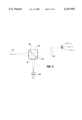
- FIG. 4 shows the construction of a first embodiment of the present invention having optical coupler element 41 cemented to optical coupler element 42 forming a single optical coupler with a coating 43 at the interface between elements 41 and 42.
- the diode laser light is collimated by either a spherical or aspheric convex surface 44 in element 41.
- the laser light is reflected from a multi-layer dielectric polarized surface 43 inclined at generally 45 degrees relative to the laser light. This dielectric coating may be applied to either of the elements 41 or 42.
- the laser is oriented such that the polarized laser light is reflected by the polarized surface 43.
- the reflected polarized laser light is focused by a convex surface 45 into a small spot.
- Surface 45 can be spherical or aspheric and may be a different contour than surface 44.
- the output optical signal may be inserted into an optical fiber 19 for sensor or duplex fiberoptic communications applications.
- Return unpolarized light is collimated by the convex surface 45 in element 42.
- the P polarization component of the returning signal is transmitted by coating 43.
- Element 42 may have a plane, spherical, or aspheric surface where the returning signal exits.
- a dichroic coating may be used instead of the polarized coating.
- the dichroic coating is specified to reflect the diode laser light and transmit the return light.
- the return light may be of a different wavelength than outgoing light in sensor applications, i.e., a fluorescence signal is measured that is of a longer wavelength than the excitation wavelength (the diode laser).
- the diode laser on each end of the fiberoptic may be of a different wavelength allowing dichroic separation. This would allow nearly 100% of the optical signals to be sensed rather than 25% using prior art spliced couplers.
- a dichroic coating may be used in the second embodiment to replace the polarized coating for the same benefits just described.
- FIG. 5 shows the construction of a second embodiment having optical coupler element 51 cemented to optical coupler element 53 with a multi-layer dielectric polarized coating 52 at the interface between elements 51 and 53.
- the diode laser light is collimated by either a spherical or aspheric convex surface 54 in element 53.
- the laser is oriented such that the laser light is transmitted through the coating 52.
- the collimated laser light is focused by convex aspheric or spherical surface 56 forming a small spot.
- the output optical signal may be inserted into an optical fiber for sensor or duplex fiberoptic communications applications.
- Returning unpolarized light is collimated by surface 56 in element 51.
- the S polarization component of the collimated returning light is reflected by surface 52.
- Element 51 may have a plane, spherical, or aspheric surface where the return light exits.
- the diode laser light is polarized and remains polarized after exiting the optical coupler.
- the light will become unpolarized after transmission through the fiber. Return light will also be unpolarized.
- the reflected light will be polarized.
- An additional element is inserted into the invention to rotate the polarization 90 degrees resulting in reflection at the internal polarized surface. This embodiment is shown in FIG. 6.
- optical coupler element 61 is bonded to a quarter wave plate 63 which is also bonded to optical coupler element 62.
- Element 62 has a multi-layer dielectric polarizing coating 64 at the planar junction of the elements, i.e., the bond interface at the quarter wave plate 63.
- P polarized diode laser light is collimated by spherical or aspheric surface 67 in element 62. This light is transmitted through coating 64.
- a quarter wave retardation plate 63 circularly polarizes the laser light.
- Aspheric or spherical surface 66 in element 61 focuses the laser light into a small spot. This laser radiation is reflected from a surface and is recollimized by surface 66 in element 61.
- the quarter wave plate 63 converts the circularly polarized returning S polarized light. This S polarized light is reflected by coating 64.
- the quarter wave plate 63 circularly polarizes the reflected light. Light exits element 61 through a plane, spherical, or aspheric surface 65.
- FIG. 7 shows another construction according to the teachings of the present invention.
- Optical coupler element 71 is bonded to optical coupler element 72.
- a multi-layer dielectric polarized coating 73 is at the interface between elements 71 and 72 and may be applied to either element.
- Light from a diode laser is collimated by surface 75 in element 72.
- Surface 75 can be spherical or aspheric.
- the diode laser is oriented such that output is P polarized and is transmitted through coating 73.
- Light from a second diode laser is collimated by surface 74 in element 71.
- the second laser is oriented such that the output is S polarized and is reflected by coating 73.
- the two beams are coincident and exit through surface 76.
- FIG. 8 illustrates optical coupler elements 71a and 72a having planar surfaces 76a and 76b and producing a collimated beam.
- FIG. 7 and FIG. 8 can be used with lasers that produce the same wavelength output or lasers with different wavelength outputs.
- a visible low power laser output can be superimposed on an invisible high power near infrared diode laser output to provide a means of visualizing the system output.
- Two identical laser beams can be combined using this invention to provide double the laser power compared to a single diode laser output.
- a dichroic coating can be substituted for the polarized coating when optical sources of two different wavelengths are combined.
- the dichroic coating is particularly beneficial when one or both sources is non-polarized. For example, light from an LED can be combined with light from a diode laser. The former is non-polarized and the later is generally polarized.
- FIG. 9 shows the construction of another embodiment.
- Laser light emitted by diode laser 96 is collimated by a convex surface in optical coupler element 91.
- the coating 92 reflects the laser light perpendicular to the laser axis.
- a convex surface in element 91 focuses the laser light into an optical fiber 97.
- Light returning through fiber 97 is collimated by the convex surface in element 91.
- Coating 92 transmits the returning light.
- a diffraction grating on face 94 of optical coupler element 93 diffracts the return light, spectrally dispersing the light.
- Lens 95 focuses the dispersed light forming a series of focused spots corresponding to various return wavelengths.
- Photodetectors (not shown) can be employed to detect the various return light signals.
- the diffraction grating 94 on element 93 in FIG. 9 can be formed by molding the grating into element 93.
- An alternative method is to replicate the diffraction pattern from a master grating into a plastic material applied to the face of element 93.
- Another alternative method is to bond a film to the face of 93 that has a diffraction grating pattern on the non-bonded surface. This diffraction grating pattern can be formed using holographic techniques or replication of a blazed master grating.
- the coating 92 between elements 91 and 93 can be applied to the hypotenuse surface of either element 91 or 93 prior to bonding these two elements together.
- the coating can be either a dichroic coating passing either wavelengths greater than or less than the diode output wavelength or it can be a polarized dielectric coating.
- the location of the incoming and exiting return signals in FIG. 9 can be reversed by using a coating that transmits rather than reflects the diode laser radiation.
- the spectrally dispersed return signal can be sensed using either a few separate photodetectors or a photodetector linear array (not shown). Spectral separation of the return signal can be used for wavelength division multiplexing for fiberoptic communications. It can be used with sensor systems to measure the intensity of various wavelength return signals.
- FIG. 10 illustrates the application of the first embodiment (FIG. 4 embodiment) in a duplex fiberoptic communications system.
- Laser light emitted from diode laser 101 is inserted into fiberoptic 107 using the invention as described with respect to the first embodiment.
- the light is transmitted through the optical fiber 107 and is transmitted by element 103 to photodetector 104.
- Light emitted by diode laser 105 is coupled into the optical fiber 107 by element 103.
- the light is transmitted through element 102 to photodiode 106.
- FIG. 11 illustrates the application of the first embodiment in a fiberoptic sensor system.
- Laser light emitted from a diode laser 110 is coupled into optical fiber 113.
- the light is transmitted to a sensing element on the far end of the fiber (not shown).
- Light is emitted or reflected by the sensing element and transmitted through element 112 to photodetector 114.
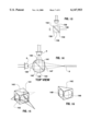
- FIG. 12 illustrates the application of the optical coupler of the type shown in FIG. 6 in an optical data storage device.
- Light from diode laser 121 is collimated by the coupler.
- the linearly polarized laser light is circularly polarized after passing through the polarizing coating and quarter wave retardation plate 124.
- the beam is focused to a small spot by a convex surface in the coupler.
- Light reflected from the optical storage media 123 is collimated by the convex surface and linearly polarized by the retardation plate.
- the returning light reflects off the polarized coating and passes through the retardation plate where it is re-circularly polarized.
- the optical elements forming this invention may be fabricated by molding or conventional grinding and polishing techniques. They may be fabricated from glass or plastic materials. Features may be fabricated into one or both elements for alignment and mounting.
- the hemispherical shapes shown in FIG. 4 and FIG. 12, for example, may be formed by grinding a sphere into a hemisphere and polishing the resultant flat face. Elements with one or more rotationally symmetric aspheric faces will most economically be fabricated using molded optics techniques.
- FIG. 13 illustrates mounting and alignment members 130, 132 formed into both optical coupler elements 136, 138. These features may be circular or planer in shape. Spherical, plane, or aspheric surfaces may be molded into the elements. The elements may contain any combination of spherical, plane, or aspheric surfaces in regions where light is transmitted or received by the element. The external surfaces may be coated with anti-reflection coatings or be uncoated.
- the two optical coupler elements of the invention are preferably fabricated from the same optical material. For some applications it may be desirable to operate with non-orthogonal axis for the detector, laser, and fiberoptic. A non-orthogonal design is achieved by using different materials for the two optical elements causing refraction at the interface between the two elements to provide rotational displacement of the optical axis.
- FIG. 14 shows a plan view of the construction of an optical coupler using aspheric surfaces 146, 147, 148 and 149 molded into a pair of right angle prisms 141, 142.
- a multi-layer dielectric polarized coating 143 is applied to the hypotenuse of one right-angle prism.
- the hypotenuse surfaces of the two prisms are bonded together using an optical adhesive.
- FIG. 14 shows an example of using two different focal length aspheric surfaces to match the numerical aperture of the diode laser source and optical fiber.
- FIG. 15 is a perspective view of the optical coupler consisting of two right angle prisms 141, 142 bonded together with spherical or rotationally symmetric surfaces molded into the exterior faces and the two prisms bonded together at their hypotenuses along the planar junction thereof having coating 143.
- FIG. 16 shows one of the optical coupler elements of FIG. 14 prior to bonding.
- the aspheric surfaces are generally rotationally symmetric with respect to the optical axis of the diode laser or detector.
- the aspheric surface is generally of a conicoidal form described by: ##EQU1## where Z is the sagital coordinate, c is the curvature, r is the radial coordinate, and k is the conic constant.
- Fiberoptic communications systems incorporate a duel-fiber transmit-receive architecture. Each fiber has a diode laser or LED coupled into one end of a fiber and photodectector on the other end of the fiber. Bi-directional communication is accomplished by placing a transmitter and receiver at each end of the fiberoptic pair. A repeater is used to extend the distance of long distance communications. A repeater consists of a receiver and transmitter in series in the optical fiber. Many fiberoptic communications systems utilize one wavelength light.
- Wavelength division multiplexing consists of replacing the single transmit source (diode laser or LED) with two or more sources along with beam combination optics to combine the beams and couple the resultant beam into an optical fiber.
- the receive optic consists of a beam splitter to separate the combined signal into individual wavelength signals and distribute them to photodetectors.
- FIG. 17 shows a wavelength division multiplexed fiberoptic communication architecture utilizing the FIG. 4 optical coupler embodiment to combine two-different wavelength sources on the transmit end of a fiberoptic communication system and also to demultiplex the two different wavelength signals on the receive end.
- the transmitter 174 consists of the coupler 171 used to multiplex two different wavelength diode lasers 172, 173.
- the multiplexed light is inserted into optical fiber 175.
- the receiver 179 consists of the coupler 176 used to demultiplex the optical signals and detect these separate wavelength signals using photodetectors 177, 178.
Landscapes
- Physics & Mathematics (AREA)
- Optics & Photonics (AREA)
- General Physics & Mathematics (AREA)
- Optical Couplings Of Light Guides (AREA)
Abstract
Description
Claims (17)
Priority Applications (1)
| Application Number | Priority Date | Filing Date | Title |
|---|---|---|---|
| US09/048,169 US6147953A (en) | 1998-03-25 | 1998-03-25 | Optical signal transmission apparatus |
Applications Claiming Priority (1)
| Application Number | Priority Date | Filing Date | Title |
|---|---|---|---|
| US09/048,169 US6147953A (en) | 1998-03-25 | 1998-03-25 | Optical signal transmission apparatus |
Publications (1)
| Publication Number | Publication Date |
|---|---|
| US6147953A true US6147953A (en) | 2000-11-14 |
Family
ID=21953096
Family Applications (1)
| Application Number | Title | Priority Date | Filing Date |
|---|---|---|---|
| US09/048,169 Expired - Fee Related US6147953A (en) | 1998-03-25 | 1998-03-25 | Optical signal transmission apparatus |
Country Status (1)
| Country | Link |
|---|---|
| US (1) | US6147953A (en) |
Cited By (72)
| Publication number | Priority date | Publication date | Assignee | Title |
|---|---|---|---|---|
| US20040085885A1 (en) * | 2002-10-31 | 2004-05-06 | Pioneer Corporation | Optical pickup, and method and apparatus for correcting aberration of optical beam |
| US20050180693A1 (en) * | 2004-02-12 | 2005-08-18 | Klingsporn Paul E. | Apparatus and method for combining light from two or more fibers into a single fiber |
| JP2005352256A (en) * | 2004-06-11 | 2005-12-22 | Fujikura Ltd | Optical component for single fiber bi-directional transmitting/receiving module and single fiber bi-directional transmitting/receiving module |
| US20090226137A1 (en) * | 2007-03-16 | 2009-09-10 | Honeywell Federal Manufacturing & Technologies, Ll | Miniature mechanical transfer optical coupler |
| US20100006873A1 (en) * | 2008-06-25 | 2010-01-14 | Soraa, Inc. | HIGHLY POLARIZED WHITE LIGHT SOURCE BY COMBINING BLUE LED ON SEMIPOLAR OR NONPOLAR GaN WITH YELLOW LED ON SEMIPOLAR OR NONPOLAR GaN |
| WO2011149977A1 (en) * | 2010-05-24 | 2011-12-01 | Soraa, Inc. | System and method of multi-wavelength laser apparatus |
| US8242522B1 (en) | 2009-05-12 | 2012-08-14 | Soraa, Inc. | Optical device structure using non-polar GaN substrates and growth structures for laser applications in 481 nm |
| US8247887B1 (en) | 2009-05-29 | 2012-08-21 | Soraa, Inc. | Method and surface morphology of non-polar gallium nitride containing substrates |
| US8254425B1 (en) | 2009-04-17 | 2012-08-28 | Soraa, Inc. | Optical device structure using GaN substrates and growth structures for laser applications |
| US8252662B1 (en) | 2009-03-28 | 2012-08-28 | Soraa, Inc. | Method and structure for manufacture of light emitting diode devices using bulk GaN |
| US8259769B1 (en) | 2008-07-14 | 2012-09-04 | Soraa, Inc. | Integrated total internal reflectors for high-gain laser diodes with high quality cleaved facets on nonpolar/semipolar GaN substrates |
| US8294179B1 (en) | 2009-04-17 | 2012-10-23 | Soraa, Inc. | Optical device structure using GaN substrates and growth structures for laser applications |
| US8314429B1 (en) | 2009-09-14 | 2012-11-20 | Soraa, Inc. | Multi color active regions for white light emitting diode |
| US8351478B2 (en) | 2009-09-17 | 2013-01-08 | Soraa, Inc. | Growth structures and method for forming laser diodes on {30-31} or off cut gallium and nitrogen containing substrates |
| US8416825B1 (en) | 2009-04-17 | 2013-04-09 | Soraa, Inc. | Optical device structure using GaN substrates and growth structure for laser applications |
| US8427590B2 (en) | 2009-05-29 | 2013-04-23 | Soraa, Inc. | Laser based display method and system |
| US8451876B1 (en) | 2010-05-17 | 2013-05-28 | Soraa, Inc. | Method and system for providing bidirectional light sources with broad spectrum |
| US8502465B2 (en) | 2009-09-18 | 2013-08-06 | Soraa, Inc. | Power light emitting diode and method with current density operation |
| US8509275B1 (en) | 2009-05-29 | 2013-08-13 | Soraa, Inc. | Gallium nitride based laser dazzling device and method |
| US8634442B1 (en) | 2009-04-13 | 2014-01-21 | Soraa Laser Diode, Inc. | Optical device structure using GaN substrates for laser applications |
| US8750342B1 (en) | 2011-09-09 | 2014-06-10 | Soraa Laser Diode, Inc. | Laser diodes with scribe structures |
| US8816319B1 (en) | 2010-11-05 | 2014-08-26 | Soraa Laser Diode, Inc. | Method of strain engineering and related optical device using a gallium and nitrogen containing active region |
| US8837545B2 (en) | 2009-04-13 | 2014-09-16 | Soraa Laser Diode, Inc. | Optical device structure using GaN substrates and growth structures for laser applications |
| US8847249B2 (en) | 2008-06-16 | 2014-09-30 | Soraa, Inc. | Solid-state optical device having enhanced indium content in active regions |
| US8975615B2 (en) | 2010-11-09 | 2015-03-10 | Soraa Laser Diode, Inc. | Method of fabricating optical devices using laser treatment of contact regions of gallium and nitrogen containing material |
| US9025635B2 (en) | 2011-01-24 | 2015-05-05 | Soraa Laser Diode, Inc. | Laser package having multiple emitters configured on a support member |
| US9046227B2 (en) | 2009-09-18 | 2015-06-02 | Soraa, Inc. | LED lamps with improved quality of light |
| US9048170B2 (en) | 2010-11-09 | 2015-06-02 | Soraa Laser Diode, Inc. | Method of fabricating optical devices using laser treatment |
| US9076926B2 (en) | 2011-08-22 | 2015-07-07 | Soraa, Inc. | Gallium and nitrogen containing trilateral configuration for optical devices |
| US9093820B1 (en) | 2011-01-25 | 2015-07-28 | Soraa Laser Diode, Inc. | Method and structure for laser devices using optical blocking regions |
| US9105806B2 (en) | 2009-03-09 | 2015-08-11 | Soraa, Inc. | Polarization direction of optical devices using selected spatial configurations |
| US9166372B1 (en) | 2013-06-28 | 2015-10-20 | Soraa Laser Diode, Inc. | Gallium nitride containing laser device configured on a patterned substrate |
| US9209596B1 (en) | 2014-02-07 | 2015-12-08 | Soraa Laser Diode, Inc. | Manufacturing a laser diode device from a plurality of gallium and nitrogen containing substrates |
| US9246311B1 (en) | 2014-11-06 | 2016-01-26 | Soraa Laser Diode, Inc. | Method of manufacture for an ultraviolet laser diode |
| CN105278115A (en) * | 2015-08-05 | 2016-01-27 | 中国科学院光电研究院 | Optical path debugging device and system of laser |
| US9250044B1 (en) | 2009-05-29 | 2016-02-02 | Soraa Laser Diode, Inc. | Gallium and nitrogen containing laser diode dazzling devices and methods of use |
| US9293644B2 (en) | 2009-09-18 | 2016-03-22 | Soraa, Inc. | Power light emitting diode and method with uniform current density operation |
| US9318875B1 (en) | 2011-01-24 | 2016-04-19 | Soraa Laser Diode, Inc. | Color converting element for laser diode |
| US9362715B2 (en) | 2014-02-10 | 2016-06-07 | Soraa Laser Diode, Inc | Method for manufacturing gallium and nitrogen bearing laser devices with improved usage of substrate material |
| US9368939B2 (en) | 2013-10-18 | 2016-06-14 | Soraa Laser Diode, Inc. | Manufacturable laser diode formed on C-plane gallium and nitrogen material |
| US9379525B2 (en) | 2014-02-10 | 2016-06-28 | Soraa Laser Diode, Inc. | Manufacturable laser diode |
| US9419189B1 (en) | 2013-11-04 | 2016-08-16 | Soraa, Inc. | Small LED source with high brightness and high efficiency |
| US9450143B2 (en) | 2010-06-18 | 2016-09-20 | Soraa, Inc. | Gallium and nitrogen containing triangular or diamond-shaped configuration for optical devices |
| US9520697B2 (en) | 2014-02-10 | 2016-12-13 | Soraa Laser Diode, Inc. | Manufacturable multi-emitter laser diode |
| US9520695B2 (en) | 2013-10-18 | 2016-12-13 | Soraa Laser Diode, Inc. | Gallium and nitrogen containing laser device having confinement region |
| US9531164B2 (en) | 2009-04-13 | 2016-12-27 | Soraa Laser Diode, Inc. | Optical device structure using GaN substrates for laser applications |
| US9564736B1 (en) | 2014-06-26 | 2017-02-07 | Soraa Laser Diode, Inc. | Epitaxial growth of p-type cladding regions using nitrogen gas for a gallium and nitrogen containing laser diode |
| US9583678B2 (en) | 2009-09-18 | 2017-02-28 | Soraa, Inc. | High-performance LED fabrication |
| US9595813B2 (en) | 2011-01-24 | 2017-03-14 | Soraa Laser Diode, Inc. | Laser package having multiple emitters configured on a substrate member |
| US9653642B1 (en) | 2014-12-23 | 2017-05-16 | Soraa Laser Diode, Inc. | Manufacturable RGB display based on thin film gallium and nitrogen containing light emitting diodes |
| US9666677B1 (en) | 2014-12-23 | 2017-05-30 | Soraa Laser Diode, Inc. | Manufacturable thin film gallium and nitrogen containing devices |
| US9787963B2 (en) | 2015-10-08 | 2017-10-10 | Soraa Laser Diode, Inc. | Laser lighting having selective resolution |
| US9800017B1 (en) | 2009-05-29 | 2017-10-24 | Soraa Laser Diode, Inc. | Laser device and method for a vehicle |
| US9829780B2 (en) | 2009-05-29 | 2017-11-28 | Soraa Laser Diode, Inc. | Laser light source for a vehicle |
| US9871350B2 (en) | 2014-02-10 | 2018-01-16 | Soraa Laser Diode, Inc. | Manufacturable RGB laser diode source |
| US9927611B2 (en) | 2010-03-29 | 2018-03-27 | Soraa Laser Diode, Inc. | Wearable laser based display method and system |
| US9978904B2 (en) | 2012-10-16 | 2018-05-22 | Soraa, Inc. | Indium gallium nitride light emitting devices |
| US10108079B2 (en) | 2009-05-29 | 2018-10-23 | Soraa Laser Diode, Inc. | Laser light source for a vehicle |
| US10222474B1 (en) | 2017-12-13 | 2019-03-05 | Soraa Laser Diode, Inc. | Lidar systems including a gallium and nitrogen containing laser light source |
| US10551728B1 (en) | 2018-04-10 | 2020-02-04 | Soraa Laser Diode, Inc. | Structured phosphors for dynamic lighting |
| US10771155B2 (en) | 2017-09-28 | 2020-09-08 | Soraa Laser Diode, Inc. | Intelligent visible light with a gallium and nitrogen containing laser source |
| US10879673B2 (en) | 2015-08-19 | 2020-12-29 | Soraa Laser Diode, Inc. | Integrated white light source using a laser diode and a phosphor in a surface mount device package |
| US10903623B2 (en) | 2019-05-14 | 2021-01-26 | Soraa Laser Diode, Inc. | Method and structure for manufacturable large area gallium and nitrogen containing substrate |
| US10938182B2 (en) | 2015-08-19 | 2021-03-02 | Soraa Laser Diode, Inc. | Specialized integrated light source using a laser diode |
| US11228158B2 (en) | 2019-05-14 | 2022-01-18 | Kyocera Sld Laser, Inc. | Manufacturable laser diodes on a large area gallium and nitrogen containing substrate |
| US11239637B2 (en) | 2018-12-21 | 2022-02-01 | Kyocera Sld Laser, Inc. | Fiber delivered laser induced white light system |
| US11421843B2 (en) | 2018-12-21 | 2022-08-23 | Kyocera Sld Laser, Inc. | Fiber-delivered laser-induced dynamic light system |
| US11437775B2 (en) | 2015-08-19 | 2022-09-06 | Kyocera Sld Laser, Inc. | Integrated light source using a laser diode |
| US11437774B2 (en) | 2015-08-19 | 2022-09-06 | Kyocera Sld Laser, Inc. | High-luminous flux laser-based white light source |
| US11677213B1 (en) | 2012-02-17 | 2023-06-13 | Kyocera Sld Laser, Inc. | Systems for photonic integration in non-polar and semi-polar oriented wave-guided optical devices |
| US11884202B2 (en) | 2019-01-18 | 2024-01-30 | Kyocera Sld Laser, Inc. | Laser-based fiber-coupled white light system |
| US12000552B2 (en) | 2019-04-10 | 2024-06-04 | Kyocera Sld Laser, Inc. | Laser-based fiber-coupled white light system for a vehicle |
Citations (17)
| Publication number | Priority date | Publication date | Assignee | Title |
|---|---|---|---|---|
| US4917014A (en) * | 1989-04-24 | 1990-04-17 | Kms Fusion, Inc. | Laser ignition of explosives |
| US5010822A (en) * | 1990-02-02 | 1991-04-30 | Whittaker Ordnance, Inc. | Explosive initiator with angled fiber optic input |
| US5095472A (en) * | 1989-06-02 | 1992-03-10 | Hitachi Cable Limited | Focusing error detecting system for optical head |
| US5124841A (en) * | 1989-10-13 | 1992-06-23 | Mitsubishi Rayon Co., Ltd. | Polarization forming optical device and polarization beam splitter |
| US5278812A (en) * | 1992-02-18 | 1994-01-11 | At&T Bell Laboratories | Tracking and focussing functions in optical disk apparatus |
| US5323378A (en) * | 1991-12-31 | 1994-06-21 | Samsung Electronics Co., Ltd. | Compact optical pickup |
| US5331622A (en) * | 1991-05-28 | 1994-07-19 | Applied Magnetics Corporation | Compact optical head |
| US5406543A (en) * | 1993-04-07 | 1995-04-11 | Olympus Optical Co., Ltd. | Optical head with semiconductor laser |
| US5467336A (en) * | 1992-12-08 | 1995-11-14 | Sony Corporation | Magneto-optical recording/reproducing apparatus with optical pickup device having a multi-layer dielectric film beam splitter |
| US5511060A (en) * | 1993-02-26 | 1996-04-23 | Industrial Technology Research Institute | Magneto-optical head with a three prism beam splitter to split a reflected beam into three beams |
| US5621714A (en) * | 1994-02-12 | 1997-04-15 | Olympus Optical Co., Ltd. | Optical pick-up apparatus having hologram and beam splitter with birefringent member and polarizing film |
| US5644563A (en) * | 1994-06-10 | 1997-07-01 | Lg Electronics Inc. | Optical pickup system |
| US5646778A (en) * | 1991-05-28 | 1997-07-08 | Discovision Associates | Optical beamsplitter |
| US5646928A (en) * | 1995-06-22 | 1997-07-08 | The Regents Of The University Of California | Free-space integrated micro-pickup head for optical data storage and a micro-optical bench |
| US5696747A (en) * | 1994-08-26 | 1997-12-09 | Eastman Kodak Company | System and method for high resolution optical recording using dual optical sources and an induced shift in media absorption |
| US5701287A (en) * | 1995-05-25 | 1997-12-23 | Sony Corporation | Optical head with a plural layers coated beam splitter for light components separation |
| US5708644A (en) * | 1996-02-28 | 1998-01-13 | Fujitsu Limited | Optical head for optical disk drive |
-
1998
- 1998-03-25 US US09/048,169 patent/US6147953A/en not_active Expired - Fee Related
Patent Citations (18)
| Publication number | Priority date | Publication date | Assignee | Title |
|---|---|---|---|---|
| US4917014A (en) * | 1989-04-24 | 1990-04-17 | Kms Fusion, Inc. | Laser ignition of explosives |
| US5095472A (en) * | 1989-06-02 | 1992-03-10 | Hitachi Cable Limited | Focusing error detecting system for optical head |
| US5124841A (en) * | 1989-10-13 | 1992-06-23 | Mitsubishi Rayon Co., Ltd. | Polarization forming optical device and polarization beam splitter |
| US5010822A (en) * | 1990-02-02 | 1991-04-30 | Whittaker Ordnance, Inc. | Explosive initiator with angled fiber optic input |
| US5646778A (en) * | 1991-05-28 | 1997-07-08 | Discovision Associates | Optical beamsplitter |
| US5331622A (en) * | 1991-05-28 | 1994-07-19 | Applied Magnetics Corporation | Compact optical head |
| US5650874A (en) * | 1991-05-28 | 1997-07-22 | Discovision Associates | Optical beamsplitter |
| US5323378A (en) * | 1991-12-31 | 1994-06-21 | Samsung Electronics Co., Ltd. | Compact optical pickup |
| US5278812A (en) * | 1992-02-18 | 1994-01-11 | At&T Bell Laboratories | Tracking and focussing functions in optical disk apparatus |
| US5467336A (en) * | 1992-12-08 | 1995-11-14 | Sony Corporation | Magneto-optical recording/reproducing apparatus with optical pickup device having a multi-layer dielectric film beam splitter |
| US5511060A (en) * | 1993-02-26 | 1996-04-23 | Industrial Technology Research Institute | Magneto-optical head with a three prism beam splitter to split a reflected beam into three beams |
| US5406543A (en) * | 1993-04-07 | 1995-04-11 | Olympus Optical Co., Ltd. | Optical head with semiconductor laser |
| US5621714A (en) * | 1994-02-12 | 1997-04-15 | Olympus Optical Co., Ltd. | Optical pick-up apparatus having hologram and beam splitter with birefringent member and polarizing film |
| US5644563A (en) * | 1994-06-10 | 1997-07-01 | Lg Electronics Inc. | Optical pickup system |
| US5696747A (en) * | 1994-08-26 | 1997-12-09 | Eastman Kodak Company | System and method for high resolution optical recording using dual optical sources and an induced shift in media absorption |
| US5701287A (en) * | 1995-05-25 | 1997-12-23 | Sony Corporation | Optical head with a plural layers coated beam splitter for light components separation |
| US5646928A (en) * | 1995-06-22 | 1997-07-08 | The Regents Of The University Of California | Free-space integrated micro-pickup head for optical data storage and a micro-optical bench |
| US5708644A (en) * | 1996-02-28 | 1998-01-13 | Fujitsu Limited | Optical head for optical disk drive |
Non-Patent Citations (2)
| Title |
|---|
| The Laser Guide Book, Hecht, J. p. 331, McGraw Hill, 1992. * |
| The Laser Guide Book, Hecht, J. p. 331, McGraw-Hill, 1992. |
Cited By (219)
| Publication number | Priority date | Publication date | Assignee | Title |
|---|---|---|---|---|
| US20040085885A1 (en) * | 2002-10-31 | 2004-05-06 | Pioneer Corporation | Optical pickup, and method and apparatus for correcting aberration of optical beam |
| US20050180693A1 (en) * | 2004-02-12 | 2005-08-18 | Klingsporn Paul E. | Apparatus and method for combining light from two or more fibers into a single fiber |
| US7013068B2 (en) | 2004-02-12 | 2006-03-14 | Honeywell Federal Manufacturing & Technologies | Apparatus and method for combining light from two or more fibers into a single fiber |
| JP2005352256A (en) * | 2004-06-11 | 2005-12-22 | Fujikura Ltd | Optical component for single fiber bi-directional transmitting/receiving module and single fiber bi-directional transmitting/receiving module |
| US20090226137A1 (en) * | 2007-03-16 | 2009-09-10 | Honeywell Federal Manufacturing & Technologies, Ll | Miniature mechanical transfer optical coupler |
| US7887243B2 (en) | 2007-03-16 | 2011-02-15 | Honeywell Federal Manufacturing & Technologies, Llc | Miniature mechanical transfer optical coupler |
| US8847249B2 (en) | 2008-06-16 | 2014-09-30 | Soraa, Inc. | Solid-state optical device having enhanced indium content in active regions |
| US20100006873A1 (en) * | 2008-06-25 | 2010-01-14 | Soraa, Inc. | HIGHLY POLARIZED WHITE LIGHT SOURCE BY COMBINING BLUE LED ON SEMIPOLAR OR NONPOLAR GaN WITH YELLOW LED ON SEMIPOLAR OR NONPOLAR GaN |
| US8259769B1 (en) | 2008-07-14 | 2012-09-04 | Soraa, Inc. | Integrated total internal reflectors for high-gain laser diodes with high quality cleaved facets on nonpolar/semipolar GaN substrates |
| US9105806B2 (en) | 2009-03-09 | 2015-08-11 | Soraa, Inc. | Polarization direction of optical devices using selected spatial configurations |
| US8252662B1 (en) | 2009-03-28 | 2012-08-28 | Soraa, Inc. | Method and structure for manufacture of light emitting diode devices using bulk GaN |
| US9722398B2 (en) | 2009-04-13 | 2017-08-01 | Soraa Laser Diode, Inc. | Optical device structure using GaN substrates for laser applications |
| US9531164B2 (en) | 2009-04-13 | 2016-12-27 | Soraa Laser Diode, Inc. | Optical device structure using GaN substrates for laser applications |
| US11862937B1 (en) | 2009-04-13 | 2024-01-02 | Kyocera Sld Laser, Inc. | Optical device structure using GaN substrates and growth structures for laser applications |
| US8969113B2 (en) | 2009-04-13 | 2015-03-03 | Soraa Laser Diode, Inc. | Optical device structure using GaN substrates and growth structures for laser applications |
| US9735547B1 (en) | 2009-04-13 | 2017-08-15 | Soraa Laser Diode, Inc. | Optical device structure using GaN substrates and growth structures for laser applications |
| US9941665B1 (en) | 2009-04-13 | 2018-04-10 | Soraa Laser Diode, Inc. | Optical device structure using GaN substrates and growth structures for laser applications |
| US10862274B1 (en) | 2009-04-13 | 2020-12-08 | Soraa Laser Diode, Inc. | Optical device structure using GaN substrates and growth structures for laser applications |
| US9356430B2 (en) | 2009-04-13 | 2016-05-31 | Soraa Laser Diode, Inc. | Optical device structure using GaN substrates and growth structures for laser applications |
| US9553426B1 (en) | 2009-04-13 | 2017-01-24 | Soraa Laser Diode, Inc. | Optical device structure using GaN substrates and growth structures for laser applications |
| US9071039B2 (en) | 2009-04-13 | 2015-06-30 | Soraa Laser Diode, Inc. | Optical device structure using GaN substrates for laser applications |
| US10374392B1 (en) | 2009-04-13 | 2019-08-06 | Soraa Laser Diode, Inc. | Optical device structure using GaN substrates and growth structures for laser applications |
| US8634442B1 (en) | 2009-04-13 | 2014-01-21 | Soraa Laser Diode, Inc. | Optical device structure using GaN substrates for laser applications |
| US8837545B2 (en) | 2009-04-13 | 2014-09-16 | Soraa Laser Diode, Inc. | Optical device structure using GaN substrates and growth structures for laser applications |
| US9099844B2 (en) | 2009-04-13 | 2015-08-04 | Soraa Laser Diode, Inc. | Optical device structure using GaN substrates and growth structures for laser applications |
| US10862273B1 (en) | 2009-04-13 | 2020-12-08 | Soraa Laser Diode, Inc. | Optical device structure using GaN substrates and growth structures for laser applications |
| US8254425B1 (en) | 2009-04-17 | 2012-08-28 | Soraa, Inc. | Optical device structure using GaN substrates and growth structures for laser applications |
| US8416825B1 (en) | 2009-04-17 | 2013-04-09 | Soraa, Inc. | Optical device structure using GaN substrates and growth structure for laser applications |
| US8294179B1 (en) | 2009-04-17 | 2012-10-23 | Soraa, Inc. | Optical device structure using GaN substrates and growth structures for laser applications |
| US8242522B1 (en) | 2009-05-12 | 2012-08-14 | Soraa, Inc. | Optical device structure using non-polar GaN substrates and growth structures for laser applications in 481 nm |
| US10205300B1 (en) | 2009-05-29 | 2019-02-12 | Soraa Laser Diode, Inc. | Gallium and nitrogen containing laser diode dazzling devices and methods of use |
| US8427590B2 (en) | 2009-05-29 | 2013-04-23 | Soraa, Inc. | Laser based display method and system |
| US8247887B1 (en) | 2009-05-29 | 2012-08-21 | Soraa, Inc. | Method and surface morphology of non-polar gallium nitride containing substrates |
| US9013638B2 (en) | 2009-05-29 | 2015-04-21 | Soraa Laser Diode, Inc. | Laser based display method and system |
| US9014229B1 (en) | 2009-05-29 | 2015-04-21 | Soraa Laser Diode, Inc. | Gallium nitride based laser dazzling method |
| US9019437B2 (en) | 2009-05-29 | 2015-04-28 | Soraa Laser Diode, Inc. | Laser based display method and system |
| US11016378B2 (en) | 2009-05-29 | 2021-05-25 | Kyocera Sld Laser, Inc. | Laser light source |
| US10904506B1 (en) | 2009-05-29 | 2021-01-26 | Soraa Laser Diode, Inc. | Laser device for white light |
| US11088507B1 (en) | 2009-05-29 | 2021-08-10 | Kyocera Sld Laser, Inc. | Laser source apparatus |
| US8837546B1 (en) | 2009-05-29 | 2014-09-16 | Soraa Laser Diode, Inc. | Gallium nitride based laser dazzling device and method |
| US9071772B2 (en) | 2009-05-29 | 2015-06-30 | Soraa Laser Diode, Inc. | Laser based display method and system |
| US11101618B1 (en) | 2009-05-29 | 2021-08-24 | Kyocera Sld Laser, Inc. | Laser device for dynamic white light |
| US9800017B1 (en) | 2009-05-29 | 2017-10-24 | Soraa Laser Diode, Inc. | Laser device and method for a vehicle |
| US9100590B2 (en) | 2009-05-29 | 2015-08-04 | Soraa Laser Diode, Inc. | Laser based display method and system |
| US8773598B2 (en) | 2009-05-29 | 2014-07-08 | Soraa Laser Diode, Inc. | Laser based display method and system |
| US11619871B2 (en) | 2009-05-29 | 2023-04-04 | Kyocera Sld Laser, Inc. | Laser based display system |
| US8509275B1 (en) | 2009-05-29 | 2013-08-13 | Soraa, Inc. | Gallium nitride based laser dazzling device and method |
| US9829778B2 (en) | 2009-05-29 | 2017-11-28 | Soraa Laser Diode, Inc. | Laser light source |
| US10297977B1 (en) | 2009-05-29 | 2019-05-21 | Soraa Laser Diode, Inc. | Laser device and method for a vehicle |
| US11796903B2 (en) | 2009-05-29 | 2023-10-24 | Kyocera Sld Laser, Inc. | Laser based display system |
| US10108079B2 (en) | 2009-05-29 | 2018-10-23 | Soraa Laser Diode, Inc. | Laser light source for a vehicle |
| US9829780B2 (en) | 2009-05-29 | 2017-11-28 | Soraa Laser Diode, Inc. | Laser light source for a vehicle |
| US9250044B1 (en) | 2009-05-29 | 2016-02-02 | Soraa Laser Diode, Inc. | Gallium and nitrogen containing laser diode dazzling devices and methods of use |
| US11817675B1 (en) | 2009-05-29 | 2023-11-14 | Kyocera Sld Laser, Inc. | Laser device for white light |
| US10084281B1 (en) | 2009-05-29 | 2018-09-25 | Soraa Laser Diode, Inc. | Laser device and method for a vehicle |
| US8908731B1 (en) | 2009-05-29 | 2014-12-09 | Soraa Laser Diode, Inc. | Gallium nitride based laser dazzling device and method |
| US8314429B1 (en) | 2009-09-14 | 2012-11-20 | Soraa, Inc. | Multi color active regions for white light emitting diode |
| US8355418B2 (en) | 2009-09-17 | 2013-01-15 | Soraa, Inc. | Growth structures and method for forming laser diodes on {20-21} or off cut gallium and nitrogen containing substrates |
| US9853420B2 (en) | 2009-09-17 | 2017-12-26 | Soraa Laser Diode, Inc. | Low voltage laser diodes on {20-21} gallium and nitrogen containing substrates |
| US10090644B2 (en) | 2009-09-17 | 2018-10-02 | Soraa Laser Diode, Inc. | Low voltage laser diodes on {20-21} gallium and nitrogen containing substrates |
| US9142935B2 (en) | 2009-09-17 | 2015-09-22 | Soraa Laser Diode, Inc. | Laser diodes with scribe structures |
| US10424900B2 (en) | 2009-09-17 | 2019-09-24 | Soraa Laser Diode, Inc. | Low voltage laser diodes on {20-21} gallium and nitrogen containing substrates |
| US8351478B2 (en) | 2009-09-17 | 2013-01-08 | Soraa, Inc. | Growth structures and method for forming laser diodes on {30-31} or off cut gallium and nitrogen containing substrates |
| US11070031B2 (en) | 2009-09-17 | 2021-07-20 | Kyocera Sld Laser, Inc. | Low voltage laser diodes on {20-21} gallium and nitrogen containing surfaces |
| US9543738B2 (en) | 2009-09-17 | 2017-01-10 | Soraa Laser Diode, Inc. | Low voltage laser diodes on {20-21} gallium and nitrogen containing substrates |
| US9293644B2 (en) | 2009-09-18 | 2016-03-22 | Soraa, Inc. | Power light emitting diode and method with uniform current density operation |
| US8502465B2 (en) | 2009-09-18 | 2013-08-06 | Soraa, Inc. | Power light emitting diode and method with current density operation |
| US9046227B2 (en) | 2009-09-18 | 2015-06-02 | Soraa, Inc. | LED lamps with improved quality of light |
| US11662067B2 (en) | 2009-09-18 | 2023-05-30 | Korrus, Inc. | LED lamps with improved quality of light |
| US10553754B2 (en) | 2009-09-18 | 2020-02-04 | Soraa, Inc. | Power light emitting diode and method with uniform current density operation |
| US10557595B2 (en) | 2009-09-18 | 2020-02-11 | Soraa, Inc. | LED lamps with improved quality of light |
| US10693041B2 (en) | 2009-09-18 | 2020-06-23 | Soraa, Inc. | High-performance LED fabrication |
| US9583678B2 (en) | 2009-09-18 | 2017-02-28 | Soraa, Inc. | High-performance LED fabrication |
| US11105473B2 (en) | 2009-09-18 | 2021-08-31 | EcoSense Lighting, Inc. | LED lamps with improved quality of light |
| US9927611B2 (en) | 2010-03-29 | 2018-03-27 | Soraa Laser Diode, Inc. | Wearable laser based display method and system |
| US11630307B2 (en) | 2010-05-17 | 2023-04-18 | Kyocera Sld Laser, Inc. | Wearable laser based display method and system |
| US10505344B1 (en) | 2010-05-17 | 2019-12-10 | Soraa Laser Diode, Inc. | Method and system for providing directional light sources with broad spectrum |
| US9362720B1 (en) | 2010-05-17 | 2016-06-07 | Soraa Laser Diode, Inc. | Method and system for providing directional light sources with broad spectrum |
| US10122148B1 (en) | 2010-05-17 | 2018-11-06 | Soraa Laser Diodide, Inc. | Method and system for providing directional light sources with broad spectrum |
| US10816801B2 (en) | 2010-05-17 | 2020-10-27 | Soraa Laser Diode, Inc. | Wearable laser based display method and system |
| US8451876B1 (en) | 2010-05-17 | 2013-05-28 | Soraa, Inc. | Method and system for providing bidirectional light sources with broad spectrum |
| US11791606B1 (en) | 2010-05-17 | 2023-10-17 | Kyocera Sld Laser, Inc. | Method and system for providing directional light sources with broad spectrum |
| US10923878B1 (en) | 2010-05-17 | 2021-02-16 | Soraa Laser Diode, Inc. | Method and system for providing directional light sources with broad spectrum |
| US9106049B1 (en) | 2010-05-17 | 2015-08-11 | Soraa Laser Diode, Inc. | Method and system for providing directional light sources with broad spectrum |
| US9837790B1 (en) | 2010-05-17 | 2017-12-05 | Soraa Laser Diode, Inc. | Method and system for providing directional light sources with broad spectrum |
| US8848755B1 (en) | 2010-05-17 | 2014-09-30 | Soraa Laser Diode, Inc. | Method and system for providing directional light sources with broad spectrum |
| WO2011149977A1 (en) * | 2010-05-24 | 2011-12-01 | Soraa, Inc. | System and method of multi-wavelength laser apparatus |
| US9450143B2 (en) | 2010-06-18 | 2016-09-20 | Soraa, Inc. | Gallium and nitrogen containing triangular or diamond-shaped configuration for optical devices |
| US11152765B1 (en) | 2010-11-05 | 2021-10-19 | Kyocera Sld Laser, Inc. | Strained and strain control regions in optical devices |
| US11715931B1 (en) | 2010-11-05 | 2023-08-01 | Kyocera Sld Laser, Inc. | Strained and strain control regions in optical devices |
| US10637210B1 (en) | 2010-11-05 | 2020-04-28 | Soraa Laser Diode, Inc. | Strained and strain control regions in optical devices |
| US10283938B1 (en) | 2010-11-05 | 2019-05-07 | Soraa Laser Diode, Inc. | Method of strain engineering and related optical device using a gallium and nitrogen containing active region |
| US9570888B1 (en) | 2010-11-05 | 2017-02-14 | Soraa Laser Diode, Inc. | Method of strain engineering and related optical device using a gallium and nitrogen containing active region |
| US9379522B1 (en) | 2010-11-05 | 2016-06-28 | Soraa Laser Diode, Inc. | Method of strain engineering and related optical device using a gallium and nitrogen containing active region |
| US8816319B1 (en) | 2010-11-05 | 2014-08-26 | Soraa Laser Diode, Inc. | Method of strain engineering and related optical device using a gallium and nitrogen containing active region |
| US9048170B2 (en) | 2010-11-09 | 2015-06-02 | Soraa Laser Diode, Inc. | Method of fabricating optical devices using laser treatment |
| US9786810B2 (en) | 2010-11-09 | 2017-10-10 | Soraa Laser Diode, Inc. | Method of fabricating optical devices using laser treatment |
| US8975615B2 (en) | 2010-11-09 | 2015-03-10 | Soraa Laser Diode, Inc. | Method of fabricating optical devices using laser treatment of contact regions of gallium and nitrogen containing material |
| US10247366B2 (en) | 2011-01-24 | 2019-04-02 | Soraa Laser Diode, Inc. | Laser package having multiple emitters configured on a support member |
| US11543590B2 (en) | 2011-01-24 | 2023-01-03 | Kyocera Sld Laser, Inc. | Optical module having multiple laser diode devices and a support member |
| US9835296B2 (en) | 2011-01-24 | 2017-12-05 | Soraa Laser Diode, Inc. | Laser package having multiple emitters configured on a support member |
| US9371970B2 (en) | 2011-01-24 | 2016-06-21 | Soraa Laser Diode, Inc. | Laser package having multiple emitters configured on a support member |
| US9025635B2 (en) | 2011-01-24 | 2015-05-05 | Soraa Laser Diode, Inc. | Laser package having multiple emitters configured on a support member |
| US9318875B1 (en) | 2011-01-24 | 2016-04-19 | Soraa Laser Diode, Inc. | Color converting element for laser diode |
| US9810383B2 (en) | 2011-01-24 | 2017-11-07 | Soraa Laser Diode, Inc. | Laser package having multiple emitters configured on a support member |
| US10655800B2 (en) | 2011-01-24 | 2020-05-19 | Soraa Laser Diode, Inc. | Laser package having multiple emitters configured on a support member |
| US11573374B2 (en) | 2011-01-24 | 2023-02-07 | Kyocera Sld Laser, Inc. | Gallium and nitrogen containing laser module configured for phosphor pumping |
| US9595813B2 (en) | 2011-01-24 | 2017-03-14 | Soraa Laser Diode, Inc. | Laser package having multiple emitters configured on a substrate member |
| US9093820B1 (en) | 2011-01-25 | 2015-07-28 | Soraa Laser Diode, Inc. | Method and structure for laser devices using optical blocking regions |
| US9076926B2 (en) | 2011-08-22 | 2015-07-07 | Soraa, Inc. | Gallium and nitrogen containing trilateral configuration for optical devices |
| US8750342B1 (en) | 2011-09-09 | 2014-06-10 | Soraa Laser Diode, Inc. | Laser diodes with scribe structures |
| US11677213B1 (en) | 2012-02-17 | 2023-06-13 | Kyocera Sld Laser, Inc. | Systems for photonic integration in non-polar and semi-polar oriented wave-guided optical devices |
| US9978904B2 (en) | 2012-10-16 | 2018-05-22 | Soraa, Inc. | Indium gallium nitride light emitting devices |
| US9887517B1 (en) | 2013-06-28 | 2018-02-06 | Soraa Laser Diode, Inc. | Gallium nitride containing laser device configured on a patterned substrate |
| US9466949B1 (en) | 2013-06-28 | 2016-10-11 | Soraa Laser Diode, Inc. | Gallium nitride containing laser device configured on a patterned substrate |
| US9166372B1 (en) | 2013-06-28 | 2015-10-20 | Soraa Laser Diode, Inc. | Gallium nitride containing laser device configured on a patterned substrate |
| US11177634B1 (en) | 2013-06-28 | 2021-11-16 | Kyocera Sld Laser, Inc. | Gallium and nitrogen containing laser device configured on a patterned substrate |
| US10186841B1 (en) | 2013-06-28 | 2019-01-22 | Soraa Laser Diode, Inc. | Gallium nitride containing laser device configured on a patterned substrate |
| US10651629B1 (en) | 2013-06-28 | 2020-05-12 | Soraa Laser Diode, Inc. | Gallium nitride containing laser device configured on a patterned substrate |
| US9882353B2 (en) | 2013-10-18 | 2018-01-30 | Soraa Laser Diode, Inc. | Gallium and nitrogen containing laser device having confinement region |
| US11569637B2 (en) | 2013-10-18 | 2023-01-31 | Kyocera Sld Laser, Inc. | Manufacturable laser diode formed on c-plane gallium and nitrogen material |
| US9774170B2 (en) | 2013-10-18 | 2017-09-26 | Soraa Laser Diode, Inc. | Manufacturable laser diode formed on C-plane gallium and nitrogen material |
| US10439364B2 (en) | 2013-10-18 | 2019-10-08 | Soraa Laser Diode, Inc. | Manufacturable laser diode formed on c-plane gallium and nitrogen material |
| US10903625B2 (en) | 2013-10-18 | 2021-01-26 | Soraa Laser Diode, Inc. | Manufacturable laser diode formed on c-plane gallium and nitrogen material |
| US9520695B2 (en) | 2013-10-18 | 2016-12-13 | Soraa Laser Diode, Inc. | Gallium and nitrogen containing laser device having confinement region |
| US9368939B2 (en) | 2013-10-18 | 2016-06-14 | Soraa Laser Diode, Inc. | Manufacturable laser diode formed on C-plane gallium and nitrogen material |
| US9419189B1 (en) | 2013-11-04 | 2016-08-16 | Soraa, Inc. | Small LED source with high brightness and high efficiency |
| US10529902B2 (en) | 2013-11-04 | 2020-01-07 | Soraa, Inc. | Small LED source with high brightness and high efficiency |
| US10274139B1 (en) | 2013-12-18 | 2019-04-30 | Soraa Laser Diode, Inc. | Patterned color converting element for laser diode |
| US9869433B1 (en) | 2013-12-18 | 2018-01-16 | Soraa Laser Diode, Inc. | Color converting element for laser diode |
| US10627055B1 (en) | 2013-12-18 | 2020-04-21 | Soraa Laser Diode, Inc. | Color converting device |
| US11649936B1 (en) | 2013-12-18 | 2023-05-16 | Kyocera Sld Laser, Inc. | Color converting element for laser device |
| US10431958B1 (en) | 2014-02-07 | 2019-10-01 | Soraa Laser Diode, Inc. | Semiconductor laser diode on tiled gallium containing material |
| US10044170B1 (en) | 2014-02-07 | 2018-08-07 | Soraa Laser Diode, Inc. | Semiconductor laser diode on tiled gallium containing material |
| US9209596B1 (en) | 2014-02-07 | 2015-12-08 | Soraa Laser Diode, Inc. | Manufacturing a laser diode device from a plurality of gallium and nitrogen containing substrates |
| US9401584B1 (en) | 2014-02-07 | 2016-07-26 | Soraa Laser Diode, Inc. | Laser diode device with a plurality of gallium and nitrogen containing substrates |
| US9762032B1 (en) | 2014-02-07 | 2017-09-12 | Soraa Laser Diode, Inc. | Semiconductor laser diode on tiled gallium containing material |
| US11342727B1 (en) | 2014-02-07 | 2022-05-24 | Kyocera Sld Laser, Inc. | Semiconductor laser diode on tiled gallium containing material |
| US10693279B1 (en) | 2014-02-07 | 2020-06-23 | Soraa Laser Diode, Inc. | Semiconductor laser diode on tiled gallium containing material |
| US10749315B2 (en) | 2014-02-10 | 2020-08-18 | Soraa Laser Diode, Inc. | Manufacturable RGB laser diode source |
| US10367334B2 (en) | 2014-02-10 | 2019-07-30 | Soraa Laser Diode, Inc. | Manufacturable laser diode |
| US10658810B2 (en) | 2014-02-10 | 2020-05-19 | Soraa Laser Diode, Inc. | Method for manufacturing gallium and nitrogen bearing laser devices with improved usage of substrate material |
| US11658456B2 (en) | 2014-02-10 | 2023-05-23 | Kyocera Sld Laser, Inc. | Manufacturable multi-emitter laser diode |
| US11011889B2 (en) | 2014-02-10 | 2021-05-18 | Kyocera Sld Laser, Inc. | Manufacturable multi-emitter laser diode |
| US9871350B2 (en) | 2014-02-10 | 2018-01-16 | Soraa Laser Diode, Inc. | Manufacturable RGB laser diode source |
| US9379525B2 (en) | 2014-02-10 | 2016-06-28 | Soraa Laser Diode, Inc. | Manufacturable laser diode |
| US11139637B2 (en) | 2014-02-10 | 2021-10-05 | Kyocera Sld Laser, Inc. | Manufacturable RGB laser diode source and system |
| US9755398B2 (en) | 2014-02-10 | 2017-09-05 | Soraa Laser Diode, Inc. | Method for manufacturing gallium and nitrogen bearing laser devices with improved usage of substrate material |
| US10566767B2 (en) | 2014-02-10 | 2020-02-18 | Soraa Laser Diode, Inc. | Manufacturable multi-emitter laser diode |
| US9362715B2 (en) | 2014-02-10 | 2016-06-07 | Soraa Laser Diode, Inc | Method for manufacturing gallium and nitrogen bearing laser devices with improved usage of substrate material |
| US11088505B2 (en) | 2014-02-10 | 2021-08-10 | Kyocera Sld Laser, Inc. | Method for manufacturing gallium and nitrogen bearing laser devices with improved usage of substrate material |
| US10141714B2 (en) | 2014-02-10 | 2018-11-27 | Soraa Laser Diode, Inc. | Method for manufacturing gallium and nitrogen bearing laser devices with improved usage of substrate material |
| US11710944B2 (en) | 2014-02-10 | 2023-07-25 | Kyocera Sld Laser, Inc. | Manufacturable RGB laser diode source and system |
| US9520697B2 (en) | 2014-02-10 | 2016-12-13 | Soraa Laser Diode, Inc. | Manufacturable multi-emitter laser diode |
| US11705689B2 (en) | 2014-02-10 | 2023-07-18 | Kyocera Sld Laser, Inc. | Gallium and nitrogen bearing dies with improved usage of substrate material |
| US9564736B1 (en) | 2014-06-26 | 2017-02-07 | Soraa Laser Diode, Inc. | Epitaxial growth of p-type cladding regions using nitrogen gas for a gallium and nitrogen containing laser diode |
| US10297979B1 (en) | 2014-06-26 | 2019-05-21 | Soraa Laser Diode, Inc. | Epitaxial growth of cladding regions for a gallium and nitrogen containing laser diode |
| US10439365B1 (en) | 2014-06-26 | 2019-10-08 | Soraa Laser Diode, Inc. | Epitaxial growth of cladding regions for a gallium and nitrogen containing laser diode |
| US9972974B1 (en) | 2014-06-26 | 2018-05-15 | Soraa Laser Diode, Inc. | Methods for fabricating light emitting devices |
| US9246311B1 (en) | 2014-11-06 | 2016-01-26 | Soraa Laser Diode, Inc. | Method of manufacture for an ultraviolet laser diode |
| US9711949B1 (en) | 2014-11-06 | 2017-07-18 | Soraa Laser Diode, Inc. | Method of manufacture for an ultraviolet laser diode |
| US10193309B1 (en) | 2014-11-06 | 2019-01-29 | Soraa Laser Diode, Inc. | Method of manufacture for an ultraviolet laser diode |
| US10720757B1 (en) | 2014-11-06 | 2020-07-21 | Soraa Lase Diode, Inc. | Method of manufacture for an ultraviolet laser diode |
| US11387629B1 (en) | 2014-11-06 | 2022-07-12 | Kyocera Sld Laser, Inc. | Intermediate ultraviolet laser diode device |
| US11862939B1 (en) | 2014-11-06 | 2024-01-02 | Kyocera Sld Laser, Inc. | Ultraviolet laser diode device |
| US10854777B1 (en) | 2014-12-23 | 2020-12-01 | Soraa Laser Diode, Inc. | Manufacturable thin film gallium and nitrogen containing semiconductor devices |
| US11955521B1 (en) | 2014-12-23 | 2024-04-09 | Kyocera Sld Laser, Inc. | Manufacturable thin film gallium and nitrogen containing devices |
| US10854778B1 (en) | 2014-12-23 | 2020-12-01 | Soraa Laser Diode, Inc. | Manufacturable display based on thin film gallium and nitrogen containing light emitting diodes |
| US9653642B1 (en) | 2014-12-23 | 2017-05-16 | Soraa Laser Diode, Inc. | Manufacturable RGB display based on thin film gallium and nitrogen containing light emitting diodes |
| US9666677B1 (en) | 2014-12-23 | 2017-05-30 | Soraa Laser Diode, Inc. | Manufacturable thin film gallium and nitrogen containing devices |
| US10854776B1 (en) | 2014-12-23 | 2020-12-01 | Soraa Laser Diode, Inc. | Manufacturable thin film gallium and nitrogen containing devices integrated with silicon electronic devices |
| US10629689B1 (en) | 2014-12-23 | 2020-04-21 | Soraa Laser Diode, Inc. | Manufacturable thin film gallium and nitrogen containing devices |
| US10002928B1 (en) | 2014-12-23 | 2018-06-19 | Soraa Laser Diode, Inc. | Manufacturable RGB display based on thin film gallium and nitrogen containing light emitting diodes |
| CN105278115A (en) * | 2015-08-05 | 2016-01-27 | 中国科学院光电研究院 | Optical path debugging device and system of laser |
| CN105278115B (en) * | 2015-08-05 | 2020-04-07 | 中国科学院光电研究院 | Light path debugging device and system of laser |
| US10879673B2 (en) | 2015-08-19 | 2020-12-29 | Soraa Laser Diode, Inc. | Integrated white light source using a laser diode and a phosphor in a surface mount device package |
| US11437775B2 (en) | 2015-08-19 | 2022-09-06 | Kyocera Sld Laser, Inc. | Integrated light source using a laser diode |
| US11437774B2 (en) | 2015-08-19 | 2022-09-06 | Kyocera Sld Laser, Inc. | High-luminous flux laser-based white light source |
| US11973308B2 (en) | 2015-08-19 | 2024-04-30 | Kyocera Sld Laser, Inc. | Integrated white light source using a laser diode and a phosphor in a surface mount device package |
| US10938182B2 (en) | 2015-08-19 | 2021-03-02 | Soraa Laser Diode, Inc. | Specialized integrated light source using a laser diode |
| US11172182B2 (en) | 2015-10-08 | 2021-11-09 | Kyocera Sld Laser, Inc. | Laser lighting having selective resolution |
| US10506210B2 (en) | 2015-10-08 | 2019-12-10 | Soraa Laser Diode, Inc. | Laser lighting having selective resolution |
| US10075688B2 (en) | 2015-10-08 | 2018-09-11 | Soraa Laser Diode, Inc. | Laser lighting having selective resolution |
| US9787963B2 (en) | 2015-10-08 | 2017-10-10 | Soraa Laser Diode, Inc. | Laser lighting having selective resolution |
| US11800077B2 (en) | 2015-10-08 | 2023-10-24 | Kyocera Sld Laser, Inc. | Laser lighting having selective resolution |
| US11502753B2 (en) | 2017-09-28 | 2022-11-15 | Kyocera Sld Laser, Inc. | Intelligent visible light with a gallium and nitrogen containing laser source |
| US11677468B2 (en) | 2017-09-28 | 2023-06-13 | Kyocera Sld Laser, Inc. | Laser based white light source configured for communication |
| US10880005B2 (en) | 2017-09-28 | 2020-12-29 | Soraa Laser Diode, Inc. | Laser based white light source configured for communication |
| US11870495B2 (en) | 2017-09-28 | 2024-01-09 | Kyocera Sld Laser, Inc. | Intelligent visible light with a gallium and nitrogen containing laser source |
| US10873395B2 (en) | 2017-09-28 | 2020-12-22 | Soraa Laser Diode, Inc. | Smart laser light for communication |
| US11277204B2 (en) | 2017-09-28 | 2022-03-15 | Kyocera Sld Laser, Inc. | Laser based white light source configured for communication |
| US11121772B2 (en) | 2017-09-28 | 2021-09-14 | Kyocera Sld Laser, Inc. | Smart laser light for a vehicle |
| US11153011B2 (en) | 2017-09-28 | 2021-10-19 | Kyocera Sld Laser, Inc. | Intelligent visible light with a gallium and nitrogen containing laser source |
| US10784960B2 (en) | 2017-09-28 | 2020-09-22 | Soraa Laser Diode, Inc. | Fiber delivered laser based white light source configured for communication |
| US10771155B2 (en) | 2017-09-28 | 2020-09-08 | Soraa Laser Diode, Inc. | Intelligent visible light with a gallium and nitrogen containing laser source |
| US10345446B2 (en) | 2017-12-13 | 2019-07-09 | Soraa Laser Diode, Inc. | Integrated laser lighting and LIDAR system |
| US11287527B2 (en) | 2017-12-13 | 2022-03-29 | Kyocera Sld Laser, Inc. | Distance detecting systems for use in mobile machines including gallium and nitrogen containing laser diodes |
| US10649086B2 (en) | 2017-12-13 | 2020-05-12 | Soraa Laser Diode, Inc. | Lidar systems including a gallium and nitrogen containing laser light source |
| US10338220B1 (en) | 2017-12-13 | 2019-07-02 | Soraa Laser Diode, Inc. | Integrated lighting and LIDAR system |
| US11231499B2 (en) | 2017-12-13 | 2022-01-25 | Kyocera Sld Laser, Inc. | Distance detecting systems for use in automotive applications including gallium and nitrogen containing laser diodes |
| US11867813B2 (en) | 2017-12-13 | 2024-01-09 | Kyocera Sld Laser, Inc. | Distance detecting systems for use in mobile machines including gallium and nitrogen containing laser diodes |
| US11199628B2 (en) | 2017-12-13 | 2021-12-14 | Kyocera Sld Laser, Inc. | Distance detecting systems including gallium and nitrogen containing laser diodes |
| US10222474B1 (en) | 2017-12-13 | 2019-03-05 | Soraa Laser Diode, Inc. | Lidar systems including a gallium and nitrogen containing laser light source |
| US11841429B2 (en) | 2017-12-13 | 2023-12-12 | Kyocera Sld Laser, Inc. | Distance detecting systems for use in mobile machine applications |
| US11249189B2 (en) | 2017-12-13 | 2022-02-15 | Kyocera Sld Laser, Inc. | Distance detecting systems for use in mobile machines including gallium and nitrogen containing laser diodes |
| US10551728B1 (en) | 2018-04-10 | 2020-02-04 | Soraa Laser Diode, Inc. | Structured phosphors for dynamic lighting |
| US11811189B1 (en) | 2018-04-10 | 2023-11-07 | Kyocera Sld Laser, Inc. | Structured phosphors for dynamic lighting |
| US10809606B1 (en) | 2018-04-10 | 2020-10-20 | Soraa Laser Diode, Inc. | Structured phosphors for dynamic lighting |
| US11294267B1 (en) | 2018-04-10 | 2022-04-05 | Kyocera Sld Laser, Inc. | Structured phosphors for dynamic lighting |
| US11239637B2 (en) | 2018-12-21 | 2022-02-01 | Kyocera Sld Laser, Inc. | Fiber delivered laser induced white light system |
| US11421843B2 (en) | 2018-12-21 | 2022-08-23 | Kyocera Sld Laser, Inc. | Fiber-delivered laser-induced dynamic light system |
| US11594862B2 (en) | 2018-12-21 | 2023-02-28 | Kyocera Sld Laser, Inc. | Fiber delivered laser induced white light system |
| US11788699B2 (en) | 2018-12-21 | 2023-10-17 | Kyocera Sld Laser, Inc. | Fiber-delivered laser-induced dynamic light system |
| US11884202B2 (en) | 2019-01-18 | 2024-01-30 | Kyocera Sld Laser, Inc. | Laser-based fiber-coupled white light system |
| US12000552B2 (en) | 2019-04-10 | 2024-06-04 | Kyocera Sld Laser, Inc. | Laser-based fiber-coupled white light system for a vehicle |
| US11228158B2 (en) | 2019-05-14 | 2022-01-18 | Kyocera Sld Laser, Inc. | Manufacturable laser diodes on a large area gallium and nitrogen containing substrate |
| US11949212B2 (en) | 2019-05-14 | 2024-04-02 | Kyocera Sld Laser, Inc. | Method for manufacturable large area gallium and nitrogen containing substrate |
| US11715927B2 (en) | 2019-05-14 | 2023-08-01 | Kyocera Sld Laser, Inc. | Manufacturable laser diodes on a large area gallium and nitrogen containing substrate |
| US10903623B2 (en) | 2019-05-14 | 2021-01-26 | Soraa Laser Diode, Inc. | Method and structure for manufacturable large area gallium and nitrogen containing substrate |
Similar Documents
| Publication | Publication Date | Title |
|---|---|---|
| US6147953A (en) | Optical signal transmission apparatus | |
| US4671613A (en) | Optical beam splitter prism | |
| AU2001276008B2 (en) | Optical fiber system | |
| US5771122A (en) | Optical beamsplitter | |
| US4904043A (en) | Optical data link dual wavelength coupler | |
| US5497438A (en) | Optical transmission and reception module having coupled optical waveguide chips | |
| US4456329A (en) | Optical device having multiple wavelength dependent optical paths | |
| US7933521B2 (en) | Integrated multiplexer/demultiplexer having offset transmitters and receivers for use in an optical transceiver module | |
| US5666448A (en) | Variable splitting optical coupler | |
| JP2001296449A (en) | Angled optical connector | |
| US10739518B2 (en) | Optical components for wavelength division multiplexing with high-density optical interconnect modules | |
| CN112235050B (en) | Single-optical-fiber bidirectional transmitting-receiving device and optical fiber communication system | |
| US20160277140A1 (en) | Optical transmitters | |
| CN112840176A (en) | Detector for determining a position of at least one object | |
| US6870988B2 (en) | Tap outlet collimator | |
| US6637947B2 (en) | Optical coupling configuration | |
| US6396981B1 (en) | Optical device module | |
| GB2413858A (en) | Optical beam-splitter with plano convex lens | |
| US6829096B1 (en) | Bi-directional wavelength division multiplexing/demultiplexing devices | |
| US7266270B2 (en) | Waveguide to waveguide monitor | |
| CN105612456B (en) | Optical module, the component including optical module and the method for manufacturing optical module | |
| WO2021026774A1 (en) | Multichannel parallel bidirectional device coupling apparatus | |
| JP2005352256A (en) | Optical component for single fiber bi-directional transmitting/receiving module and single fiber bi-directional transmitting/receiving module | |
| CN109669249B (en) | Dual-wavelength bidirectional transmission optical assembly and method | |
| JP2000338359A (en) | Optical monitor module |
Legal Events
| Date | Code | Title | Description |
|---|---|---|---|
| AS | Assignment |
Owner name: DUNCAN TECHNOLOGIES, INC., CALIFORNIA Free format text: ASSIGNMENT OF ASSIGNORS INTEREST;ASSIGNOR:DUNCAN, DAVID;REEL/FRAME:009066/0704 Effective date: 19980318 |
|
| AS | Assignment |
Owner name: NATIONAL AERONAUTICS AND SPACE ADMIN, DISTRICT OF Free format text: CONFIRMATORY LICENSE;ASSIGNOR:DUNCAN TECHNOLOGIES, INC.;REEL/FRAME:009661/0216 Effective date: 19980901 |
|
| FEPP | Fee payment procedure |
Free format text: PAT HOLDER NO LONGER CLAIMS SMALL ENTITY STATUS, ENTITY STATUS SET TO UNDISCOUNTED (ORIGINAL EVENT CODE: STOL); ENTITY STATUS OF PATENT OWNER: LARGE ENTITY |
|
| REFU | Refund |
Free format text: REFUND - SURCHARGE, PETITION TO ACCEPT PYMT AFTER EXP, UNINTENTIONAL (ORIGINAL EVENT CODE: R2551); ENTITY STATUS OF PATENT OWNER: LARGE ENTITY Free format text: REFUND - SURCHARGE FOR LATE PAYMENT, SMALL ENTITY (ORIGINAL EVENT CODE: R2554); ENTITY STATUS OF PATENT OWNER: LARGE ENTITY |
|
| REMI | Maintenance fee reminder mailed | ||
| FPAY | Fee payment |
Year of fee payment: 4 |
|
| SULP | Surcharge for late payment | ||
| REMI | Maintenance fee reminder mailed | ||
| LAPS | Lapse for failure to pay maintenance fees | ||
| STCH | Information on status: patent discontinuation |
Free format text: PATENT EXPIRED DUE TO NONPAYMENT OF MAINTENANCE FEES UNDER 37 CFR 1.362 |
|
| FP | Lapsed due to failure to pay maintenance fee |
Effective date: 20081114 |