US6147378A - Fully recessed semiconductor device and method for low power applications with single wrap around buried drain region - Google Patents
Fully recessed semiconductor device and method for low power applications with single wrap around buried drain region Download PDFInfo
- Publication number
- US6147378A US6147378A US09/052,060 US5206098A US6147378A US 6147378 A US6147378 A US 6147378A US 5206098 A US5206098 A US 5206098A US 6147378 A US6147378 A US 6147378A
- Authority
- US
- United States
- Prior art keywords
- trench
- region
- buried
- trenched
- substrate
- Prior art date
- Legal status (The legal status is an assumption and is not a legal conclusion. Google has not performed a legal analysis and makes no representation as to the accuracy of the status listed.)
- Expired - Fee Related
Links
- 239000004065 semiconductor Substances 0.000 title claims abstract description 79
- 238000000034 method Methods 0.000 title abstract description 18
- 239000000758 substrate Substances 0.000 claims abstract description 74
- 238000009792 diffusion process Methods 0.000 claims description 17
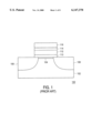
- 238000012876 topography Methods 0.000 abstract description 4
- 239000010410 layer Substances 0.000 description 82
- 229910021420 polycrystalline silicon Inorganic materials 0.000 description 21
- 229920005591 polysilicon Polymers 0.000 description 21
- 239000007943 implant Substances 0.000 description 11
- 239000012535 impurity Substances 0.000 description 10
- 150000004767 nitrides Chemical class 0.000 description 10
- 239000002019 doping agent Substances 0.000 description 9
- WQJQOUPTWCFRMM-UHFFFAOYSA-N tungsten disilicide Chemical compound [Si]#[W]#[Si] WQJQOUPTWCFRMM-UHFFFAOYSA-N 0.000 description 8
- 229910021342 tungsten silicide Inorganic materials 0.000 description 8
- XUIMIQQOPSSXEZ-UHFFFAOYSA-N Silicon Chemical compound [Si] XUIMIQQOPSSXEZ-UHFFFAOYSA-N 0.000 description 7
- 230000015572 biosynthetic process Effects 0.000 description 7
- 229910052710 silicon Inorganic materials 0.000 description 7
- 239000010703 silicon Substances 0.000 description 7
- 239000000463 material Substances 0.000 description 5
- 230000015654 memory Effects 0.000 description 5
- 125000006850 spacer group Chemical group 0.000 description 5
- ZOXJGFHDIHLPTG-UHFFFAOYSA-N Boron Chemical compound [B] ZOXJGFHDIHLPTG-UHFFFAOYSA-N 0.000 description 4
- 229910052796 boron Inorganic materials 0.000 description 4
- 238000000151 deposition Methods 0.000 description 4
- BHEPBYXIRTUNPN-UHFFFAOYSA-N hydridophosphorus(.) (triplet) Chemical compound [PH] BHEPBYXIRTUNPN-UHFFFAOYSA-N 0.000 description 4
- 239000011229 interlayer Substances 0.000 description 4
- 238000004519 manufacturing process Methods 0.000 description 4
- 229910052785 arsenic Inorganic materials 0.000 description 3
- RQNWIZPPADIBDY-UHFFFAOYSA-N arsenic atom Chemical compound [As] RQNWIZPPADIBDY-UHFFFAOYSA-N 0.000 description 3
- 238000005530 etching Methods 0.000 description 3
- 238000005468 ion implantation Methods 0.000 description 3
- 238000012856 packing Methods 0.000 description 3
- WFKWXMTUELFFGS-UHFFFAOYSA-N tungsten Chemical compound [W] WFKWXMTUELFFGS-UHFFFAOYSA-N 0.000 description 3
- 229910052721 tungsten Inorganic materials 0.000 description 3
- 239000010937 tungsten Substances 0.000 description 3
- BOTDANWDWHJENH-UHFFFAOYSA-N Tetraethyl orthosilicate Chemical compound CCO[Si](OCC)(OCC)OCC BOTDANWDWHJENH-UHFFFAOYSA-N 0.000 description 2
- 238000005229 chemical vapour deposition Methods 0.000 description 2
- 239000004020 conductor Substances 0.000 description 2
- 230000008878 coupling Effects 0.000 description 2
- 238000010168 coupling process Methods 0.000 description 2
- 238000005859 coupling reaction Methods 0.000 description 2
- 239000013078 crystal Substances 0.000 description 2
- 230000008021 deposition Effects 0.000 description 2
- 238000002347 injection Methods 0.000 description 2
- 239000007924 injection Substances 0.000 description 2
- 238000004518 low pressure chemical vapour deposition Methods 0.000 description 2
- 230000035945 sensitivity Effects 0.000 description 2
- 208000032750 Device leakage Diseases 0.000 description 1
- 230000005689 Fowler Nordheim tunneling Effects 0.000 description 1
- 229910007277 Si3 N4 Inorganic materials 0.000 description 1
- 229910052581 Si3N4 Inorganic materials 0.000 description 1
- 238000007796 conventional method Methods 0.000 description 1
- 239000003989 dielectric material Substances 0.000 description 1
- 230000000694 effects Effects 0.000 description 1
- 238000002513 implantation Methods 0.000 description 1
- 238000011065 in-situ storage Methods 0.000 description 1
- 238000002955 isolation Methods 0.000 description 1
- 230000000873 masking effect Effects 0.000 description 1
- 229910021421 monocrystalline silicon Inorganic materials 0.000 description 1
- 230000003647 oxidation Effects 0.000 description 1
- 238000007254 oxidation reaction Methods 0.000 description 1
- 238000000059 patterning Methods 0.000 description 1
- 229920002120 photoresistant polymer Polymers 0.000 description 1
- 238000005498 polishing Methods 0.000 description 1
- HQVNEWCFYHHQES-UHFFFAOYSA-N silicon nitride Chemical compound N12[Si]34N5[Si]62N3[Si]51N64 HQVNEWCFYHHQES-UHFFFAOYSA-N 0.000 description 1
Images


Classifications
-
- H—ELECTRICITY
- H01—ELECTRIC ELEMENTS
- H01L—SEMICONDUCTOR DEVICES NOT COVERED BY CLASS H10
- H01L29/00—Semiconductor devices adapted for rectifying, amplifying, oscillating or switching, or capacitors or resistors with at least one potential-jump barrier or surface barrier, e.g. PN junction depletion layer or carrier concentration layer; Details of semiconductor bodies or of electrodes thereof ; Multistep manufacturing processes therefor
- H01L29/66—Types of semiconductor device ; Multistep manufacturing processes therefor
- H01L29/66007—Multistep manufacturing processes
- H01L29/66075—Multistep manufacturing processes of devices having semiconductor bodies comprising group 14 or group 13/15 materials
- H01L29/66227—Multistep manufacturing processes of devices having semiconductor bodies comprising group 14 or group 13/15 materials the devices being controllable only by the electric current supplied or the electric potential applied, to an electrode which does not carry the current to be rectified, amplified or switched, e.g. three-terminal devices
- H01L29/66409—Unipolar field-effect transistors
- H01L29/66477—Unipolar field-effect transistors with an insulated gate, i.e. MISFET
- H01L29/66825—Unipolar field-effect transistors with an insulated gate, i.e. MISFET with a floating gate
-
- H—ELECTRICITY
- H01—ELECTRIC ELEMENTS
- H01L—SEMICONDUCTOR DEVICES NOT COVERED BY CLASS H10
- H01L29/00—Semiconductor devices adapted for rectifying, amplifying, oscillating or switching, or capacitors or resistors with at least one potential-jump barrier or surface barrier, e.g. PN junction depletion layer or carrier concentration layer; Details of semiconductor bodies or of electrodes thereof ; Multistep manufacturing processes therefor
- H01L29/40—Electrodes ; Multistep manufacturing processes therefor
- H01L29/41—Electrodes ; Multistep manufacturing processes therefor characterised by their shape, relative sizes or dispositions
- H01L29/423—Electrodes ; Multistep manufacturing processes therefor characterised by their shape, relative sizes or dispositions not carrying the current to be rectified, amplified or switched
- H01L29/42312—Gate electrodes for field effect devices
- H01L29/42316—Gate electrodes for field effect devices for field-effect transistors
- H01L29/4232—Gate electrodes for field effect devices for field-effect transistors with insulated gate
- H01L29/42324—Gate electrodes for transistors with a floating gate
- H01L29/42336—Gate electrodes for transistors with a floating gate with one gate at least partly formed in a trench
-
- H—ELECTRICITY
- H01—ELECTRIC ELEMENTS
- H01L—SEMICONDUCTOR DEVICES NOT COVERED BY CLASS H10
- H01L29/00—Semiconductor devices adapted for rectifying, amplifying, oscillating or switching, or capacitors or resistors with at least one potential-jump barrier or surface barrier, e.g. PN junction depletion layer or carrier concentration layer; Details of semiconductor bodies or of electrodes thereof ; Multistep manufacturing processes therefor
- H01L29/66—Types of semiconductor device ; Multistep manufacturing processes therefor
- H01L29/68—Types of semiconductor device ; Multistep manufacturing processes therefor controllable by only the electric current supplied, or only the electric potential applied, to an electrode which does not carry the current to be rectified, amplified or switched
- H01L29/76—Unipolar devices, e.g. field effect transistors
- H01L29/772—Field effect transistors
- H01L29/78—Field effect transistors with field effect produced by an insulated gate
- H01L29/788—Field effect transistors with field effect produced by an insulated gate with floating gate
- H01L29/7881—Programmable transistors with only two possible levels of programmation
- H01L29/7883—Programmable transistors with only two possible levels of programmation charging by tunnelling of carriers, e.g. Fowler-Nordheim tunnelling
-
- Y—GENERAL TAGGING OF NEW TECHNOLOGICAL DEVELOPMENTS; GENERAL TAGGING OF CROSS-SECTIONAL TECHNOLOGIES SPANNING OVER SEVERAL SECTIONS OF THE IPC; TECHNICAL SUBJECTS COVERED BY FORMER USPC CROSS-REFERENCE ART COLLECTIONS [XRACs] AND DIGESTS
- Y10—TECHNICAL SUBJECTS COVERED BY FORMER USPC
- Y10S—TECHNICAL SUBJECTS COVERED BY FORMER USPC CROSS-REFERENCE ART COLLECTIONS [XRACs] AND DIGESTS
- Y10S257/00—Active solid-state devices, e.g. transistors, solid-state diodes
- Y10S257/905—Plural dram cells share common contact or common trench
Abstract
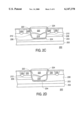
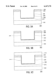
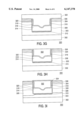
Description
Claims (14)
Priority Applications (2)
| Application Number | Priority Date | Filing Date | Title |
|---|---|---|---|
| US09/052,060 US6147378A (en) | 1998-03-30 | 1998-03-30 | Fully recessed semiconductor device and method for low power applications with single wrap around buried drain region |
| US09/470,568 US6225161B1 (en) | 1998-03-30 | 1999-12-22 | Fully recessed semiconductor method for low power applications with single wrap around buried drain region |
Applications Claiming Priority (1)
| Application Number | Priority Date | Filing Date | Title |
|---|---|---|---|
| US09/052,060 US6147378A (en) | 1998-03-30 | 1998-03-30 | Fully recessed semiconductor device and method for low power applications with single wrap around buried drain region |
Related Child Applications (1)
| Application Number | Title | Priority Date | Filing Date |
|---|---|---|---|
| US09/470,568 Division US6225161B1 (en) | 1998-03-30 | 1999-12-22 | Fully recessed semiconductor method for low power applications with single wrap around buried drain region |
Publications (1)
| Publication Number | Publication Date |
|---|---|
| US6147378A true US6147378A (en) | 2000-11-14 |
Family
ID=21975188
Family Applications (2)
| Application Number | Title | Priority Date | Filing Date |
|---|---|---|---|
| US09/052,060 Expired - Fee Related US6147378A (en) | 1998-03-30 | 1998-03-30 | Fully recessed semiconductor device and method for low power applications with single wrap around buried drain region |
| US09/470,568 Expired - Lifetime US6225161B1 (en) | 1998-03-30 | 1999-12-22 | Fully recessed semiconductor method for low power applications with single wrap around buried drain region |
Family Applications After (1)
| Application Number | Title | Priority Date | Filing Date |
|---|---|---|---|
| US09/470,568 Expired - Lifetime US6225161B1 (en) | 1998-03-30 | 1999-12-22 | Fully recessed semiconductor method for low power applications with single wrap around buried drain region |
Country Status (1)
| Country | Link |
|---|---|
| US (2) | US6147378A (en) |
Cited By (19)
| Publication number | Priority date | Publication date | Assignee | Title |
|---|---|---|---|---|
| US6239465B1 (en) * | 1999-01-27 | 2001-05-29 | Fujitsu, Ltd. | Non-volatile semiconductor memory device having vertical transistors with the floating and control gates in a trench and fabrication method therefor |
| US6284608B1 (en) * | 2000-02-01 | 2001-09-04 | Advanced Micro Devices, Inc. | Method for making accumulation mode N-channel SOI |
| US6465836B2 (en) * | 2001-03-29 | 2002-10-15 | Taiwan Semiconductor Manufacturing Co., Ltd | Vertical split gate field effect transistor (FET) device |
| US6469345B2 (en) * | 2000-01-14 | 2002-10-22 | Denso Corporation | Semiconductor device and method for manufacturing the same |
| US20030001204A1 (en) * | 2001-06-27 | 2003-01-02 | Mitsubishi Denki Kabushiki Kaisha | Semiconductor device and method for fabricating the same |
| US20030148575A1 (en) * | 2000-12-19 | 2003-08-07 | Micron Technology, Inc. | Methods of accessing floating-gate memory cells having underlying source-line connections |
| US20040071016A1 (en) * | 2000-11-02 | 2004-04-15 | Oliver Gehring | Semiconductor memory cell and method for producing the same |
| US20040248407A1 (en) * | 2003-06-05 | 2004-12-09 | Chi-Wen Liu | Displacement method to grow cu overburden |
| US6864532B2 (en) | 2000-01-14 | 2005-03-08 | Denso Corporation | Semiconductor device and method for manufacturing the same |
| US20050151185A1 (en) * | 2003-12-31 | 2005-07-14 | Jung Jin H. | Semiconductor device and fabricating method thereof |
| US20060186458A1 (en) * | 2005-02-23 | 2006-08-24 | Micron Technology,Inc. | Germanium-silicon-carbide floating gates in memories |
| US20070210403A1 (en) * | 2006-03-07 | 2007-09-13 | Micron Technology, Inc. | Isolation regions and their formation |
| US7372096B2 (en) | 2001-08-30 | 2008-05-13 | Micron Technology, Inc. | Programmable array logic or memory with p-channel devices and asymmetrical tunnel barriers |
| US7443715B2 (en) | 2001-08-30 | 2008-10-28 | Micron Technology, Inc. | SRAM cells with repressed floating gate memory, low tunnel barrier interpoly insulators |
| US7465983B2 (en) | 2001-08-30 | 2008-12-16 | Micron Technology, Inc. | Low tunnel barrier insulators |
| US7545674B2 (en) | 2001-08-30 | 2009-06-09 | Micron Technology, Inc. | Flash memory with low tunnel barrier interpoly insulators |
| US7572695B2 (en) | 2005-05-27 | 2009-08-11 | Micron Technology, Inc. | Hafnium titanium oxide films |
| US20120056258A1 (en) * | 2010-09-06 | 2012-03-08 | Shu-Lu Chen | Electrical switch using gated resistor structures and three-dimensional integrated circuits using the same |
| CN108321192A (en) * | 2018-02-05 | 2018-07-24 | 电子科技大学 | A kind of two-way trench gate charge storage type IGBT and preparation method thereof |
Families Citing this family (3)
| Publication number | Priority date | Publication date | Assignee | Title |
|---|---|---|---|---|
| US6417050B1 (en) * | 2000-08-07 | 2002-07-09 | Semiconductor Components Industries Llc | Semiconductor component and method of manufacture |
| US8058687B2 (en) * | 2007-01-30 | 2011-11-15 | Alpha & Omega Semiconductor, Ltd. | Split gate with different gate materials and work functions to reduce gate resistance of ultra high density MOSFET |
| US8664713B2 (en) | 2008-12-31 | 2014-03-04 | Stmicroelectronics S.R.L. | Integrated power device on a semiconductor substrate having an improved trench gate structure |
Citations (15)
| Publication number | Priority date | Publication date | Assignee | Title |
|---|---|---|---|---|
| US35810A (en) * | 1862-07-08 | Improved clothes-wringer | ||
| US4271418A (en) * | 1979-10-29 | 1981-06-02 | American Microsystems, Inc. | VMOS Memory cell and method for making same |
| US4835741A (en) * | 1986-06-02 | 1989-05-30 | Texas Instruments Incorporated | Frasable electrically programmable read only memory cell using a three dimensional trench floating gate |
| US5146426A (en) * | 1990-11-08 | 1992-09-08 | North American Philips Corp. | Electrically erasable and programmable read only memory with trench structure |
| US5315142A (en) * | 1992-03-23 | 1994-05-24 | International Business Machines Corporation | High performance trench EEPROM cell |
| US5341342A (en) * | 1992-12-18 | 1994-08-23 | National Semiconductor Corporation | Flash memory cell structure |
| US5429970A (en) * | 1994-07-18 | 1995-07-04 | United Microelectronics Corporation | Method of making flash EEPROM memory cell |
| US5488244A (en) * | 1995-02-27 | 1996-01-30 | Chartered Simiconductor Manufacturing Pte Ltd. | Electrically erasable and programmable read only memory cell |
| US5729496A (en) * | 1994-07-30 | 1998-03-17 | Lg Semicon Co., Ltd. | Nonvolatile semiconductor memory element and method for fabricating the same |
| US5770484A (en) * | 1996-12-13 | 1998-06-23 | International Business Machines Corporation | Method of making silicon on insulator buried plate trench capacitor |
| US5801075A (en) * | 1996-10-30 | 1998-09-01 | Advanced Micro Devices, Inc. | Method of forming trench transistor with metal spacers |
| US5854114A (en) * | 1997-10-09 | 1998-12-29 | Advanced Micro Devices, Inc. | Data retention of EEPROM cell with shallow trench isolation using thicker liner oxide |
| US5859459A (en) * | 1996-04-03 | 1999-01-12 | Sony Corporation | Semiconductor memory device and method of manufacturing the same |
| US5915180A (en) * | 1994-04-06 | 1999-06-22 | Denso Corporation | Process for producing a semiconductor device having a single thermal oxidizing step |
| US5923063A (en) * | 1998-02-19 | 1999-07-13 | Advanced Micro Devices, Inc. | Double density V nonvolatile memory cell |
Family Cites Families (5)
| Publication number | Priority date | Publication date | Assignee | Title |
|---|---|---|---|---|
| US4979004A (en) | 1988-01-29 | 1990-12-18 | Texas Instruments Incorporated | Floating gate memory cell and device |
| DE3816358A1 (en) | 1988-05-13 | 1989-11-23 | Eurosil Electronic Gmbh | NON-VOLATILE STORAGE CELL AND METHOD FOR THE PRODUCTION THEREOF |
| US5281548A (en) | 1992-07-28 | 1994-01-25 | Micron Technology, Inc. | Plug-based floating gate memory |
| US5897343A (en) * | 1998-03-30 | 1999-04-27 | Motorola, Inc. | Method of making a power switching trench MOSFET having aligned source regions |
| US5990515A (en) * | 1998-03-30 | 1999-11-23 | Advanced Micro Devices, Inc. | Trenched gate non-volatile semiconductor device and method with corner doping and sidewall doping |
-
1998
- 1998-03-30 US US09/052,060 patent/US6147378A/en not_active Expired - Fee Related
-
1999
- 1999-12-22 US US09/470,568 patent/US6225161B1/en not_active Expired - Lifetime
Patent Citations (15)
| Publication number | Priority date | Publication date | Assignee | Title |
|---|---|---|---|---|
| US35810A (en) * | 1862-07-08 | Improved clothes-wringer | ||
| US4271418A (en) * | 1979-10-29 | 1981-06-02 | American Microsystems, Inc. | VMOS Memory cell and method for making same |
| US4835741A (en) * | 1986-06-02 | 1989-05-30 | Texas Instruments Incorporated | Frasable electrically programmable read only memory cell using a three dimensional trench floating gate |
| US5146426A (en) * | 1990-11-08 | 1992-09-08 | North American Philips Corp. | Electrically erasable and programmable read only memory with trench structure |
| US5315142A (en) * | 1992-03-23 | 1994-05-24 | International Business Machines Corporation | High performance trench EEPROM cell |
| US5341342A (en) * | 1992-12-18 | 1994-08-23 | National Semiconductor Corporation | Flash memory cell structure |
| US5915180A (en) * | 1994-04-06 | 1999-06-22 | Denso Corporation | Process for producing a semiconductor device having a single thermal oxidizing step |
| US5429970A (en) * | 1994-07-18 | 1995-07-04 | United Microelectronics Corporation | Method of making flash EEPROM memory cell |
| US5729496A (en) * | 1994-07-30 | 1998-03-17 | Lg Semicon Co., Ltd. | Nonvolatile semiconductor memory element and method for fabricating the same |
| US5488244A (en) * | 1995-02-27 | 1996-01-30 | Chartered Simiconductor Manufacturing Pte Ltd. | Electrically erasable and programmable read only memory cell |
| US5859459A (en) * | 1996-04-03 | 1999-01-12 | Sony Corporation | Semiconductor memory device and method of manufacturing the same |
| US5801075A (en) * | 1996-10-30 | 1998-09-01 | Advanced Micro Devices, Inc. | Method of forming trench transistor with metal spacers |
| US5770484A (en) * | 1996-12-13 | 1998-06-23 | International Business Machines Corporation | Method of making silicon on insulator buried plate trench capacitor |
| US5854114A (en) * | 1997-10-09 | 1998-12-29 | Advanced Micro Devices, Inc. | Data retention of EEPROM cell with shallow trench isolation using thicker liner oxide |
| US5923063A (en) * | 1998-02-19 | 1999-07-13 | Advanced Micro Devices, Inc. | Double density V nonvolatile memory cell |
Cited By (46)
| Publication number | Priority date | Publication date | Assignee | Title |
|---|---|---|---|---|
| US6391721B2 (en) | 1999-01-27 | 2002-05-21 | Fujitsu Limited | Non-volatile semiconductor memory device having vertical transistors and fabrication method therefor |
| US6239465B1 (en) * | 1999-01-27 | 2001-05-29 | Fujitsu, Ltd. | Non-volatile semiconductor memory device having vertical transistors with the floating and control gates in a trench and fabrication method therefor |
| US6469345B2 (en) * | 2000-01-14 | 2002-10-22 | Denso Corporation | Semiconductor device and method for manufacturing the same |
| US7354829B2 (en) | 2000-01-14 | 2008-04-08 | Denso Corporation | Trench-gate transistor with ono gate dielectric and fabrication process therefor |
| US20050090060A1 (en) * | 2000-01-14 | 2005-04-28 | Takaaki Aoki | Method for manufacturing semiconductor device |
| US6864532B2 (en) | 2000-01-14 | 2005-03-08 | Denso Corporation | Semiconductor device and method for manufacturing the same |
| US6284608B1 (en) * | 2000-02-01 | 2001-09-04 | Advanced Micro Devices, Inc. | Method for making accumulation mode N-channel SOI |
| US20040071016A1 (en) * | 2000-11-02 | 2004-04-15 | Oliver Gehring | Semiconductor memory cell and method for producing the same |
| US6940121B2 (en) * | 2000-11-02 | 2005-09-06 | Infineon Technology Ag | Semiconductor memory cell |
| US6774426B2 (en) | 2000-12-19 | 2004-08-10 | Micron Technology, Inc. | Flash cell with trench source-line connection |
| US7176077B2 (en) | 2000-12-19 | 2007-02-13 | Micron Technology, Inc. | Methods of forming memory cells and arrays having underlying source-line connections |
| US6721206B2 (en) | 2000-12-19 | 2004-04-13 | Micron Technology, Inc. | Methods of accessing floating-gate memory cells having underlying source-line connections |
| US20040262671A1 (en) * | 2000-12-19 | 2004-12-30 | Micron Technology, Inc. | Flash cell with trench source-line connection |
| US20030148575A1 (en) * | 2000-12-19 | 2003-08-07 | Micron Technology, Inc. | Methods of accessing floating-gate memory cells having underlying source-line connections |
| US20050148141A1 (en) * | 2000-12-19 | 2005-07-07 | Micron Technology, Inc. | Methods of forming memory cells and arrays having underlying source-line connections |
| US20070117299A1 (en) * | 2000-12-19 | 2007-05-24 | Micron Technology, Inc. | Memory cells having underlying source-line connections |
| US6929993B2 (en) | 2000-12-19 | 2005-08-16 | Micron Technology, Inc. | Methods of forming memory cells and arrays having underlying source-line connections |
| US6949791B2 (en) | 2000-12-19 | 2005-09-27 | Micron Technology, Inc. | Flash cell with trench source-line connection |
| US6465836B2 (en) * | 2001-03-29 | 2002-10-15 | Taiwan Semiconductor Manufacturing Co., Ltd | Vertical split gate field effect transistor (FET) device |
| US6700159B2 (en) * | 2001-06-27 | 2004-03-02 | Renesas Technology Corp. | Semiconductor device comprising trench-isolated transistors |
| US20030001204A1 (en) * | 2001-06-27 | 2003-01-02 | Mitsubishi Denki Kabushiki Kaisha | Semiconductor device and method for fabricating the same |
| US7508025B2 (en) | 2001-08-30 | 2009-03-24 | Micron Technology, Inc. | Atomic layer deposition of metal oxide and/or low asymmetrical tunnel barrier interpoly insulators |
| US7545674B2 (en) | 2001-08-30 | 2009-06-09 | Micron Technology, Inc. | Flash memory with low tunnel barrier interpoly insulators |
| US7759724B2 (en) | 2001-08-30 | 2010-07-20 | Micron Technology, Inc. | Memory cells having gate structure with multiple gates and multiple materials between the gates |
| US7504687B2 (en) | 2001-08-30 | 2009-03-17 | Micron Technology, Inc. | Atomic layer deposition of metal oxide and/or low asymmetrical tunnel barrier interpoly insulators |
| US7473956B2 (en) | 2001-08-30 | 2009-01-06 | Micron Technology, Inc. | Atomic layer deposition of metal oxide and/or low assymmetrical tunnel barrier interpoly insulators |
| US7372096B2 (en) | 2001-08-30 | 2008-05-13 | Micron Technology, Inc. | Programmable array logic or memory with p-channel devices and asymmetrical tunnel barriers |
| US7372097B2 (en) | 2001-08-30 | 2008-05-13 | Micron Technology, Inc. | Programmable array logic or memory with p-channel devices and asymmetrical tunnel barriers |
| US7391072B2 (en) | 2001-08-30 | 2008-06-24 | Micron Technology, Inc. | Programmable array logic or memory with p-channel devices and asymmetrical tunnel barriers |
| US7443715B2 (en) | 2001-08-30 | 2008-10-28 | Micron Technology, Inc. | SRAM cells with repressed floating gate memory, low tunnel barrier interpoly insulators |
| US7465983B2 (en) | 2001-08-30 | 2008-12-16 | Micron Technology, Inc. | Low tunnel barrier insulators |
| US6903011B2 (en) * | 2003-06-05 | 2005-06-07 | Taiwan Semiconductor Manufacturing Company, Ltd. | Displacement method to grow cu overburden |
| US20040248407A1 (en) * | 2003-06-05 | 2004-12-09 | Chi-Wen Liu | Displacement method to grow cu overburden |
| US20050151185A1 (en) * | 2003-12-31 | 2005-07-14 | Jung Jin H. | Semiconductor device and fabricating method thereof |
| US20060186458A1 (en) * | 2005-02-23 | 2006-08-24 | Micron Technology,Inc. | Germanium-silicon-carbide floating gates in memories |
| US8330202B2 (en) | 2005-02-23 | 2012-12-11 | Micron Technology, Inc. | Germanium-silicon-carbide floating gates in memories |
| US7572695B2 (en) | 2005-05-27 | 2009-08-11 | Micron Technology, Inc. | Hafnium titanium oxide films |
| US7700989B2 (en) | 2005-05-27 | 2010-04-20 | Micron Technology, Inc. | Hafnium titanium oxide films |
| US20070210403A1 (en) * | 2006-03-07 | 2007-09-13 | Micron Technology, Inc. | Isolation regions and their formation |
| US7811935B2 (en) * | 2006-03-07 | 2010-10-12 | Micron Technology, Inc. | Isolation regions and their formation |
| US20110024822A1 (en) * | 2006-03-07 | 2011-02-03 | Micron Technology, Inc. | Isolation regions |
| US8269306B2 (en) * | 2006-03-07 | 2012-09-18 | Micron Technology, Inc. | Isolation regions |
| US20120056258A1 (en) * | 2010-09-06 | 2012-03-08 | Shu-Lu Chen | Electrical switch using gated resistor structures and three-dimensional integrated circuits using the same |
| US8653598B2 (en) * | 2010-09-06 | 2014-02-18 | Shu-Lu Chen | Electrical switch using gated resistor structures and three-dimensional integrated circuits using the same |
| CN108321192A (en) * | 2018-02-05 | 2018-07-24 | 电子科技大学 | A kind of two-way trench gate charge storage type IGBT and preparation method thereof |
| CN108321192B (en) * | 2018-02-05 | 2020-08-28 | 电子科技大学 | Bidirectional trench gate charge storage type IGBT and manufacturing method thereof |
Also Published As
| Publication number | Publication date |
|---|---|
| US6225161B1 (en) | 2001-05-01 |
Similar Documents
| Publication | Publication Date | Title |
|---|---|---|
| US6147377A (en) | Fully recessed semiconductor device | |
| US6147378A (en) | Fully recessed semiconductor device and method for low power applications with single wrap around buried drain region | |
| US6225659B1 (en) | Trenched gate semiconductor device and method for low power applications | |
| US5049515A (en) | Method of making a three-dimensional memory cell with integral select transistor | |
| US4964080A (en) | Three-dimensional memory cell with integral select transistor | |
| US5087584A (en) | Process for fabricating a contactless floating gate memory array utilizing wordline trench vias | |
| US5420060A (en) | Method of making contract-free floating-gate memory array with silicided buried bitlines and with single-step defined floating gates | |
| US5284785A (en) | Diffusionless source/drain conductor electrically-erasable, electrically-programmable read-only memory and methods for making and using the same | |
| US5110753A (en) | Cross-point contact-free floating-gate memory array with silicided buried bitlines | |
| US7163863B2 (en) | Vertical memory cell and manufacturing method thereof | |
| US20030067032A1 (en) | Process for manufacturing a dual charge storage location memory cell | |
| US7126188B2 (en) | Vertical split gate memory cell and manufacturing method thereof | |
| US6168994B1 (en) | Method of making memory device with an element splitting trench | |
| US5923063A (en) | Double density V nonvolatile memory cell | |
| JP2000357784A (en) | Nonvolatile semiconductor memory and manufacture thereof | |
| US5990515A (en) | Trenched gate non-volatile semiconductor device and method with corner doping and sidewall doping | |
| US5023680A (en) | Floating-gate memory array with silicided buried bitlines and with single-step-defined floating gates | |
| US6730959B1 (en) | Structure of flash memory device and fabrication method thereof | |
| US6285054B1 (en) | Trenched gate non-volatile semiconductor device with the source/drain regions spaced from the trench by sidewall dopings | |
| US6194269B1 (en) | Method to improve cell performance in split gate flash EEPROM | |
| US5120571A (en) | Floating-gate memory array with silicided buried bitlines and with single-step-defined floating gates | |
| US5200350A (en) | Floating-gate memory array with silicided buried bitlines | |
| US6806143B2 (en) | Self-aligned source pocket for flash memory cells | |
| US5238855A (en) | Cross-point contact-free array with a high-density floating-gate structure | |
| WO2000051188A1 (en) | Flash memory cell with self-aligned gates and fabrication process |
Legal Events
| Date | Code | Title | Description |
|---|---|---|---|
| AS | Assignment |
Owner name: ADVANCED MICRO DEVICES, INC., CALIFORNIA Free format text: ASSIGNMENT OF ASSIGNORS INTEREST;ASSIGNORS:LIU, YOWJUANG WILLIAM;WOLLESEN, DONALD L.;REEL/FRAME:009078/0592;SIGNING DATES FROM 19980317 TO 19980327 |
|
| FPAY | Fee payment |
Year of fee payment: 4 |
|
| AS | Assignment |
Owner name: SPANSION INC., CALIFORNIA Free format text: ASSIGNMENT OF ASSIGNORS INTEREST;ASSIGNOR:ADVANCED MICRO DEVICES, INC.;REEL/FRAME:019028/0623 Effective date: 20070131 |
|
| AS | Assignment |
Owner name: SPANSION LLC, CALIFORNIA Free format text: ASSIGNMENT OF ASSIGNORS INTEREST;ASSIGNOR:SPANSION INC.;REEL/FRAME:019069/0028 Effective date: 20070131 |
|
| REMI | Maintenance fee reminder mailed | ||
| LAPS | Lapse for failure to pay maintenance fees | ||
| STCH | Information on status: patent discontinuation |
Free format text: PATENT EXPIRED DUE TO NONPAYMENT OF MAINTENANCE FEES UNDER 37 CFR 1.362 |
|
| FP | Lapsed due to failure to pay maintenance fee |
Effective date: 20081114 |
|
| AS | Assignment |
Owner name: BARCLAYS BANK PLC,NEW YORK Free format text: SECURITY AGREEMENT;ASSIGNORS:SPANSION LLC;SPANSION INC.;SPANSION TECHNOLOGY INC.;AND OTHERS;REEL/FRAME:024522/0338 Effective date: 20100510 Owner name: BARCLAYS BANK PLC, NEW YORK Free format text: SECURITY AGREEMENT;ASSIGNORS:SPANSION LLC;SPANSION INC.;SPANSION TECHNOLOGY INC.;AND OTHERS;REEL/FRAME:024522/0338 Effective date: 20100510 |
|
| AS | Assignment |
Owner name: SPANSION LLC, CALIFORNIA Free format text: RELEASE BY SECURED PARTY;ASSIGNOR:BARCLAYS BANK PLC;REEL/FRAME:035201/0159 Effective date: 20150312 Owner name: SPANSION TECHNOLOGY LLC, CALIFORNIA Free format text: RELEASE BY SECURED PARTY;ASSIGNOR:BARCLAYS BANK PLC;REEL/FRAME:035201/0159 Effective date: 20150312 Owner name: SPANSION INC., CALIFORNIA Free format text: RELEASE BY SECURED PARTY;ASSIGNOR:BARCLAYS BANK PLC;REEL/FRAME:035201/0159 Effective date: 20150312 |
|
| AS | Assignment |
Owner name: CYPRESS SEMICONDUCTOR CORPORATION, CALIFORNIA Free format text: ASSIGNMENT OF ASSIGNORS INTEREST;ASSIGNOR:SPANSION, LLC;REEL/FRAME:036017/0625 Effective date: 20150601 |
|
| AS | Assignment |
Owner name: SPANSION LLC, CALIFORNIA Free format text: PARTIAL RELEASE OF SECURITY INTEREST IN PATENTS;ASSIGNOR:MORGAN STANLEY SENIOR FUNDING, INC., AS COLLATERAL AGENT;REEL/FRAME:039708/0001 Effective date: 20160811 Owner name: CYPRESS SEMICONDUCTOR CORPORATION, CALIFORNIA Free format text: PARTIAL RELEASE OF SECURITY INTEREST IN PATENTS;ASSIGNOR:MORGAN STANLEY SENIOR FUNDING, INC., AS COLLATERAL AGENT;REEL/FRAME:039708/0001 Effective date: 20160811 |
|
| AS | Assignment |
Owner name: MONTEREY RESEARCH, LLC, CALIFORNIA Free format text: ASSIGNMENT OF ASSIGNORS INTEREST;ASSIGNOR:CYPRESS SEMICONDUCTOR CORPORATION;REEL/FRAME:040911/0238 Effective date: 20160811 |