US6141023A - Efficient display flip - Google Patents
Efficient display flip Download PDFInfo
- Publication number
- US6141023A US6141023A US09/016,795 US1679598A US6141023A US 6141023 A US6141023 A US 6141023A US 1679598 A US1679598 A US 1679598A US 6141023 A US6141023 A US 6141023A
- Authority
- US
- United States
- Prior art keywords
- display
- graphics
- status
- flip
- next frame
- Prior art date
- Legal status (The legal status is an assumption and is not a legal conclusion. Google has not performed a legal analysis and makes no representation as to the accuracy of the status listed.)
- Expired - Lifetime
Links
Images


Classifications
-
- G—PHYSICS
- G09—EDUCATION; CRYPTOGRAPHY; DISPLAY; ADVERTISING; SEALS
- G09G—ARRANGEMENTS OR CIRCUITS FOR CONTROL OF INDICATING DEVICES USING STATIC MEANS TO PRESENT VARIABLE INFORMATION
- G09G5/00—Control arrangements or circuits for visual indicators common to cathode-ray tube indicators and other visual indicators
- G09G5/36—Control arrangements or circuits for visual indicators common to cathode-ray tube indicators and other visual indicators characterised by the display of a graphic pattern, e.g. using an all-points-addressable [APA] memory
- G09G5/363—Graphics controllers
Definitions
- the present invention is related to the field of memory access, more specifically, the present invention is a method and apparatus for an efficient display flip for a graphics device.
- Smooth motion graphics is desirable for display of computer graphics such as for three dimensional animation.
- a primary display engine of a graphics device on a computer must be provided with successive next frame data in a timely manner.
- a display flip refers to when a primary display engine of a graphics device is ready to process a next frame data for display on a display device.
- a graphics driver for the graphics device typically provides information for the next frame to be displayed to the graphics device after a display flip occurs.
- a processor is required to notify the graphics driver of the display flip status by accessing internal registers of the graphics device to determine when a display flip has occurred. This approach typically involves the processor sending a request to the graphics device.
- Display flips occur successively while the primary display engine is processing next frame data for display.
- the processor is therefore required to initiate numerous read operations to the graphics device for display flip status requiring both processor as well as bus time.
- the prior art therefore takes bus processing time away from other devices and processor time away from other applications.
- a method and apparatus is therefore desired which obviate the need for the processor to perform reads to internal registers in the graphics while still making the display flip information available to the graphics driver.
- the apparatus has a computer readable medium having a graphics driver.
- the execution of the graphics driver is configured to generate instructions for checking status of a graphics device to determine whether the graphics device is ready to display a next frame data on a display device.
- the graphics device is coupled to a system memory.
- the graphics device is configured to forwarding a display flip status to the system memory for access by the graphics driver in response to the instructions.
- FIG. 1 is a system block diagram illustrating the present invention's graphics device.
- FIG. 2 is one embodiment of a process flow of the graphics device.
- FIG. 3 illustrates a command stream controller of the graphics device.
- FIG. 4 is a state machine illustrating the function of the present invention's front buffer instruction and store double word instruction.
- FIGS. 5A and 5B are flow diagrams illustrating the general steps followed by the present invention.
- the present invention is a method and apparatus for an efficient display flip.
- a display flip refers to when a primary display engine is ready to process a next frame data for display.
- the present invention obviates the need for a graphics driver to have a processor fetch the display flip status from the graphics device. More specifically, the present invention provides the display flip status to a cacheable location in system memory for easy access by the graphics driver.
- FIG. 1 is a system block diagram illustrating the present invention's graphics device.
- a display flip indicates that a primary display engine (not shown) of a graphics device 100 is ready to process the next frame data for display.
- the graphics device 100 processes a plurality of next frame data 103 1 . . . 103 N stored in a local memory 105 for display.
- the next frame data 103 1 . . . 103 N are processed for display on a computer monitor 104 or a television 106 through an encoder 108.
- the present invention's graphics device 100 is capable of accessing system memory 114 with cacheable memory 116 through peripheral component interconnect (PCI) devices 120 1 . . . 120 N .
- PCI devices 120 1 . . . 120 N are input/output hardware devices that are connected to the system through, for example, a PCI expansion connector (not shown).
- PCI devices include but are not limited to a graphics controller/card, a disk controller/card, a local area network (LAN) controller/card and a video controller/card.
- the AGP 111 is a point to point connection between the graphics device 100 and a host bridge 110 and is designed to optimize the graphics data transfer operations in high speed personal computers (PC).
- the host bridge 110 allows various devices including the graphics device 100, the processor 118 and the peripheral component interconnect (PCI) devices 120 1 . . . 120 N to retrieve and forward data to and from the system memory 114.
- PCI peripheral component interconnect
- the processor 118 is coupled to the host bridge 110 through a bus 115.
- the system memory 114 is coupled to the host bridge 110 through a bus 117.
- the PCI devices 120 1 . . . 120 N are coupled to the host bridge 110 through a bus 119.
- the processor 118 may be a Pentium® II processor.
- a graphics driver 101 generates graphics instructions, graphics data, staring address of graphics data and graphics status information for use by the graphics device. Once generated, the graphics instructions and graphics (next frame) data are forwarded to the AGP 111 for storage in the graphics device's local memory 105 including internal registers. The start address and status information are forwarded to the PCI devices 120 1 . . . 120 N for storage in a cacheable memory 116 in the system memory 114.
- the cacheable memory 116 has a first predetermined address 122 and a second predetermined address 123 for storing display flip status information accessible by the graphics driver 101.
- FIG. 2 is a block diagram of the graphics device of the present invention.
- the graphics driver generates a front buffer instruction and a store double word instruction to facilitate the successive processing of next frame data by the primary display engine 208 for display of smooth motion computer graphics.
- the next frame data is located in local memory.
- the front buffer instruction provides the starting address of the next frame data to the primary display engine 208.
- the graphics driver begins polling a second predetermined address in cacheable memory until feedback is returned indicating that both the front buffer and the store double word instructions have been processed.
- the instructions are forwarded to a data stream controller 202 through an AGP/PCI interface block 200.
- the data stream controller 202 consists of a number of units which handle the interface between the primary display engine 208 and the AGP/PCI ports.
- the AGP/PCI interface block 200 facilitates the transmission of data between the data stream controller 202 and the AGP and the PCI bus.
- the two instructions are processed by a command stream controller 204 of the data stream controller 202.
- the command stream controller 204 is the instruction decoder for the graphics device and is described in detail in FIG. 3 and the accompanying text.
- FIG. 3 illustrates an exemplary command stream controller of the present invention.
- the front buffer instruction is first forwarded to the command stream controller of the graphics device.
- the store double word instruction is generated after the front buffer instruction and is also forwarded to the command stream controller.
- the command stream controller processes the store double word instruction after it processes the front buffer instruction.
- the instructions are decoded by a PCI decoder 304 and transmitted to either a low priority instruction first-in first-out (FIFO) 306 or a high priority instruction FIFO 308 depending upon the priority of the instruction being processed. Priority is predetermined by the system designers of the particular computer system being designed. If the instructions are received through an AGP unit 302 of the command stream controller, the instructions are sent to a direct memory access (DMA) FIFO 309.
- DMA direct memory access
- the first instruction transmitted for processing is the front buffer instruction.
- the front buffer instruction which has the starting address of the next frame data is parsed through a command parser 310.
- the command parser 310 forwards the starting address of the next frame data to the primary display engine.
- the primary display engine stores the starting address in a register (not shown) until it is ready to process the next frame data.
- the front buffer instruction also causes an interrupt status register 317 to be updated in an operating register block 316. More specifically, the front buffer instruction causes the command parser to generate a bit change operation which changes a display flip status bit in the interrupt status register 317 from a 0 to a 1 indicating that a display flip is pending in the primary display engine.
- the command parser 310 After the interrupt status register 317 is updated, the command parser 310 performs a PCI master write 312 of the display flip status bit to a first predetermined address in cacheable memory.
- the first predetermined address is designated by a hardware status vector address register 318 of the operating registers 316.
- the store double word instruction generated by the graphics driver is also forwarded to the command parser 310 of the command controller following the front buffer instruction.
- the store double word instruction causes the command parser 310 to generate another PCI master write 312 of a instruction completion indicator data to a second predetermined address in cacheable memory.
- the second predetermined address and the instruction completion indicator data are provided by the store double word instruction.
- the PCI unit 300 Upon receiving the instruction completion indicator data through the PCI master write 312, the PCI unit 300 writes the instruction completion indicator data to the second predetermined address in cacheable memory. Once the instruction completion indicator data has been written to the second predetermined address, the graphics driver which has been polling the second predetermined address finds the instruction completion indicator data and is therefore notified that both the front buffer instruction and the store double word instruction have been processed by the graphics device.
- the graphics driver then begins to poll the first predetermined address in cacheable memory until it finds the display flip status bit in the first predetermined address changed from a 1 to a 0 indicating that a display flip has occurred.
- the primary display engine While the graphics driver is polling the first predetermined address, the primary display engine may become ready to process the next frame data. Once the primary display engine is ready to process the next frame data, the primary display engine generates a vertical synchronization signal.
- the vertical synchronization signal causes the command parser 310 to generate a bit change operation which changes the display flip status bit in the interrupt status register from a 1 to a 0 indicating that a display flip has occurred.
- the status change in the interrupt register causes the command parser 310 to perform a PCI master write 312 to the first predetermined address in cacheable memory which changes the status bit in the first predetermined address from a 1 to a 0 indicating that a display flip has occurred.
- the graphics driver which has been polling the first predetermined address in cacheable memory finds that the status bit has changed from a 1 to a 0 indicating that a display flip has occurred.
- the graphics driver may now initiate the processing of a new frame data by generating a new front buffer instruction followed by a new store double word instruction and the process repeats until there are no more next frame data to process.
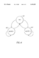
- FIG. 4 is a state machine illustrating the functions of the present invention's front buffer instruction and store double word instruction.
- the state machine has two portions. Namely, the transition between state 401 and state 402 represents state changes caused by the front buffer instruction and the transition between state 401 and state 403 represents state changes caused by the store double word instruction.
- the state machine transitions from an idle state 401 to a master write state 402.
- the front buffer instruction causes the command parser to generate a bit change operation which changes the display flip status bit from a 0 to a 1 in an interrupt status register indicating that a display flip is pending.
- the front buffer instruction also causes the command parser to generate a PCI master write to a first predetermined address in cacheable memory.
- the first predetermined address is provided by a hardware status vector address register.
- the status bit in the first predetermined address is changed from a 0 to a 1 indicating that a display is pending.
- the state machine returns to an idle state 401 and waits in this state until the primary display engine is ready to process a next frame data.
- a store double word instruction generated by the graphics driver transitions the other half of the state machine from an idle state 401 to a master write 403.
- the store double word instruction causes a second PCI master write to be performed.
- the state machine waits in this state until the write operation occurs.
- the second PCI master write writes an instruction completion indicator data in a second predetermined address in cacheable memory to indicate that the front buffer instruction has been processed.
- the second predetermined address and the instruction completion indicator data is provided by the store double word instruction.
- the state transitions from a master write state 403 back to an idle state 401.
- the graphics driver then begins polling the first predetermined address in cacheable memory until the status bit changes from a 1 to a 0 indicating that the display flip has occurred.
- a vertical synchronization signal is generated by the primary display engine when the primary display engine is ready to process the data for the next frame to be displayed.
- the primary display engine flips and takes the starting address provided by the front buffer instruction and fetches the next frame data from local memory.
- the generation of the vertical synchronization signal causes the command parser to generate a bit change operation.
- the bit change operation causes the status bit in the interrupt status register to change from a 1 to a 0 indicating that a display flip has occurred.
- the command parser In response to the change in the status bit in the interrupt status register, the command parser generates a PCI master write of the new status bit to the first predetermined address in cacheable memory and the state transitions from an idle state 401 to a master write state 402.
- the PCI unit acknowledges the PCI master write and the state machine returns to the idle state 401 when the write of the new status bit to the first predetermined address in cacheable memory completes.
- the graphics driver finds that the display flip status bit in the first predetermined address in cacheable memory has changed from 1 to a 0 indicating that a display flip has occurred.
- the graphics driver generates a new front buffer instruction for the next frame data and the entire process repeats for subsequent next frame data.
- FIG. 5 is a flow diagram illustrating the general steps followed by the present invention.
- the graphics driver for the graphics device generates a front buffer instruction in preparation for the next frame data to be processed by the graphics device and initializes a second predetermined address in cacheable memory.
- the front buffer instruction is provided to the graphics device through its AGP/PCI interface and transmitted to the command parser of the graphics device.
- step 502 in response to the front buffer instruction, the command parser generates a bit change operation in the operating register block.
- the status bit of the interrupt status register in the operating register is changed from a 0 to a 1 implying that a display flip is pending in the primary display engine.
- step 504 in response to the change in the status bit of the interrupt status register, the operating register block generates a PCI master write signal which enables a PCI write to a first predetermined address in cacheable memory provided by a hardware status vector address register also resident in the operating register.
- a store double word instruction is generated by the graphics driver to the graphics device through the AGP/PCI interface and is forwarded to the command parser of the graphics device.
- the command parser in response to the store double word instruction, the command parser generates a second PCI master write which is to a second predetermined address in cacheable memory for an instruction completion indicator data to notify the graphics driver that the front buffer instruction has been processed by the graphics device and that a display flip is now pending.
- step 507 once the store double word instruction has completed its write operation, the graphics driver begins polling the first predetermined address specified by the hardware status vector address register to determine whether the first predetermined address in cacheable memory contains a status bit of 0 indicating that the display flip has occurred.
- step 508 once the primary display engine is ready for the next frame data, the primary display engine generates a vertical synchronization signal and fetches the next frame data from the front buffer address in local memory.
- the vertical synchronization signal causes the status bit in the interrupt register to change from a 1 to a 0 indicating that the display flip has occurred.
- the change in the status bit in the interrupt status register causes a PCI master write of the status bit in the first predetermined address in memory from a 1 to a 0 indicating that the display flip has occurred.
- step 512 the graphics driver finds that the status bit in the first predetermined address in memory is a 0 indicating that the display flip has occurred. The graphics driver then generates a new front buffer instruction for the next frame data and the process repeats for each successive next frame data to be processed by the primary display engine of the graphics device.
- the present invention overcomes the disadvantages of the prior art approach by having the graphics device report its status to cacheable memory.
- the graphics driver therefore only needs to poll cacheable locations in system memory for the display flip status.
Abstract
Description
Claims (16)
Priority Applications (1)
| Application Number | Priority Date | Filing Date | Title |
|---|---|---|---|
| US09/016,795 US6141023A (en) | 1998-01-30 | 1998-01-30 | Efficient display flip |
Applications Claiming Priority (1)
| Application Number | Priority Date | Filing Date | Title |
|---|---|---|---|
| US09/016,795 US6141023A (en) | 1998-01-30 | 1998-01-30 | Efficient display flip |
Publications (1)
| Publication Number | Publication Date |
|---|---|
| US6141023A true US6141023A (en) | 2000-10-31 |
Family
ID=21779020
Family Applications (1)
| Application Number | Title | Priority Date | Filing Date |
|---|---|---|---|
| US09/016,795 Expired - Lifetime US6141023A (en) | 1998-01-30 | 1998-01-30 | Efficient display flip |
Country Status (1)
| Country | Link |
|---|---|
| US (1) | US6141023A (en) |
Cited By (13)
| Publication number | Priority date | Publication date | Assignee | Title |
|---|---|---|---|---|
| US20030052888A1 (en) * | 2001-09-18 | 2003-03-20 | Rai Barinder Singh | Graphics controller for high speed transmission of memory read commands |
| US20030063127A1 (en) * | 2001-09-13 | 2003-04-03 | Ernst Rudolf O. | High resolution display of large electronically stored or communicated images with real time roaming |
| US20050210405A1 (en) * | 2001-09-13 | 2005-09-22 | Pixia Corp. | Image display system |
| US20060067039A1 (en) * | 2004-09-30 | 2006-03-30 | Williams Mitch A | Adjustable portable computer |
| US20060250403A1 (en) * | 2000-11-28 | 2006-11-09 | Nintendo Co., Ltd. | Graphics system interface |
| US20080278595A1 (en) * | 2007-05-11 | 2008-11-13 | Advance Micro Devices, Inc. | Video Data Capture and Streaming |
| US20090016430A1 (en) * | 2007-05-11 | 2009-01-15 | Advance Micro Devices, Inc. | Software Video Encoder with GPU Acceleration |
| US20090060032A1 (en) * | 2007-05-11 | 2009-03-05 | Advanced Micro Devices, Inc. | Software Video Transcoder with GPU Acceleration |
| US20100073371A1 (en) * | 2008-09-25 | 2010-03-25 | Pixia Corp. | Large format video archival, storage, and retrieval system and method |
| US20110229040A1 (en) * | 2010-03-16 | 2011-09-22 | Pixia Corp. | Method and system for converting an image |
| US20120007872A1 (en) * | 2008-10-02 | 2012-01-12 | Aleksandar Filipov | Method And Computer Program For Operation Of A Multi-Buffer Graphics Memory Refresh, Multi-Buffer Graphics Memory Arrangement And Communication Apparatus |
| US8532397B1 (en) | 2010-09-16 | 2013-09-10 | Pixia Corp. | Method of creating a container file for large format imagery and organizing data within the container file |
| US9407876B1 (en) | 2010-09-14 | 2016-08-02 | Pixia Corp. | Method and system for encoding and decoding multiple wide-area surveillance area-of-interest video codestreams |
Citations (4)
| Publication number | Priority date | Publication date | Assignee | Title |
|---|---|---|---|---|
| US4598384A (en) * | 1983-04-22 | 1986-07-01 | International Business Machines Corp. | Graphics display with improved window organization |
| US5440746A (en) * | 1992-11-06 | 1995-08-08 | Seiko Epson Corporation | System and method for synchronizing processors in a parallel processing environment |
| US5481276A (en) * | 1992-02-03 | 1996-01-02 | Hewlett-Packard Company | Device independent interface for graphics display devices |
| US5745761A (en) * | 1994-12-15 | 1998-04-28 | International Business Machines Corporation | Advanced graphics driver architecture with extension capability |
-
1998
- 1998-01-30 US US09/016,795 patent/US6141023A/en not_active Expired - Lifetime
Patent Citations (4)
| Publication number | Priority date | Publication date | Assignee | Title |
|---|---|---|---|---|
| US4598384A (en) * | 1983-04-22 | 1986-07-01 | International Business Machines Corp. | Graphics display with improved window organization |
| US5481276A (en) * | 1992-02-03 | 1996-01-02 | Hewlett-Packard Company | Device independent interface for graphics display devices |
| US5440746A (en) * | 1992-11-06 | 1995-08-08 | Seiko Epson Corporation | System and method for synchronizing processors in a parallel processing environment |
| US5745761A (en) * | 1994-12-15 | 1998-04-28 | International Business Machines Corporation | Advanced graphics driver architecture with extension capability |
Cited By (51)
| Publication number | Priority date | Publication date | Assignee | Title |
|---|---|---|---|---|
| US20060250403A1 (en) * | 2000-11-28 | 2006-11-09 | Nintendo Co., Ltd. | Graphics system interface |
| US8984438B2 (en) | 2001-09-13 | 2015-03-17 | Pixia Corp. | Image Display System |
| US7840908B2 (en) * | 2001-09-13 | 2010-11-23 | Pixia Corp. | High resolution display of large electronically stored or communicated images with real time roaming |
| US9177525B2 (en) | 2001-09-13 | 2015-11-03 | Pixia Corp. | Image display system |
| US7607106B2 (en) | 2001-09-13 | 2009-10-20 | Pixia Corp. | Image display system |
| US20030063127A1 (en) * | 2001-09-13 | 2003-04-03 | Ernst Rudolf O. | High resolution display of large electronically stored or communicated images with real time roaming |
| US8341548B2 (en) | 2001-09-13 | 2012-12-25 | Pixia Corp. | Image display system |
| US20050210405A1 (en) * | 2001-09-13 | 2005-09-22 | Pixia Corp. | Image display system |
| US6806881B2 (en) * | 2001-09-18 | 2004-10-19 | Seiko Epson Corporation | Graphics controller for high speed transmission of memory read commands |
| US20030052888A1 (en) * | 2001-09-18 | 2003-03-20 | Rai Barinder Singh | Graphics controller for high speed transmission of memory read commands |
| US20080019088A1 (en) * | 2004-09-30 | 2008-01-24 | Intel Corporation | Adjustable portable computer |
| US7251128B2 (en) | 2004-09-30 | 2007-07-31 | Intel Corporation | Adjustable portable computer |
| US7643275B2 (en) | 2004-09-30 | 2010-01-05 | Intel Corporation | Adjustable portable computer |
| US20060067039A1 (en) * | 2004-09-30 | 2006-03-30 | Williams Mitch A | Adjustable portable computer |
| US20080278595A1 (en) * | 2007-05-11 | 2008-11-13 | Advance Micro Devices, Inc. | Video Data Capture and Streaming |
| US20090016430A1 (en) * | 2007-05-11 | 2009-01-15 | Advance Micro Devices, Inc. | Software Video Encoder with GPU Acceleration |
| US8861591B2 (en) | 2007-05-11 | 2014-10-14 | Advanced Micro Devices, Inc. | Software video encoder with GPU acceleration |
| US8233527B2 (en) | 2007-05-11 | 2012-07-31 | Advanced Micro Devices, Inc. | Software video transcoder with GPU acceleration |
| US8731046B2 (en) | 2007-05-11 | 2014-05-20 | Advanced Micro Devices, Inc. | Software video transcoder with GPU acceleration |
| US20090060032A1 (en) * | 2007-05-11 | 2009-03-05 | Advanced Micro Devices, Inc. | Software Video Transcoder with GPU Acceleration |
| US8644690B2 (en) | 2008-09-25 | 2014-02-04 | Pixia Corp. | Large format video archival, storage, and retrieval system |
| US8290346B2 (en) | 2008-09-25 | 2012-10-16 | Pixia Corp. | Large format video archival, storage, and retrieval system and method |
| US20100073371A1 (en) * | 2008-09-25 | 2010-03-25 | Pixia Corp. | Large format video archival, storage, and retrieval system and method |
| US20120007872A1 (en) * | 2008-10-02 | 2012-01-12 | Aleksandar Filipov | Method And Computer Program For Operation Of A Multi-Buffer Graphics Memory Refresh, Multi-Buffer Graphics Memory Arrangement And Communication Apparatus |
| US9684848B2 (en) | 2010-03-16 | 2017-06-20 | Pixia Corp. | System and method for retrieving an image containing image statistical data |
| US8411970B2 (en) | 2010-03-16 | 2013-04-02 | Pixia Corp. | Method and system for determining statistical data for image pixels having a higher bit depth per band |
| US10565254B2 (en) | 2010-03-16 | 2020-02-18 | Pixia Corp. | System and method for storing points of polygons related to an image |
| US20110229040A1 (en) * | 2010-03-16 | 2011-09-22 | Pixia Corp. | Method and system for converting an image |
| US10311098B2 (en) | 2010-03-16 | 2019-06-04 | Pixia Corp. | System and method for storing points of polygons related to an image |
| US9489729B2 (en) | 2010-03-16 | 2016-11-08 | Pixia Corp. | Method and system for storing statistical data of an image |
| US9407876B1 (en) | 2010-09-14 | 2016-08-02 | Pixia Corp. | Method and system for encoding and decoding multiple wide-area surveillance area-of-interest video codestreams |
| US11044437B2 (en) | 2010-09-14 | 2021-06-22 | Pixia Corp. | Method and system for combining multiple area-of-interest video codestreams into a combined video codestream |
| US10681305B2 (en) | 2010-09-14 | 2020-06-09 | Pixia Corp. | Method and system for combining multiple area-of-interest video codestreams into a combined video codestream |
| US9621904B2 (en) | 2010-09-14 | 2017-04-11 | Pixia Corp. | Method and system for transmitting multiple wide-area surveillance area-of-interest video codestreams |
| US9058642B2 (en) | 2010-09-16 | 2015-06-16 | Pixia Corp. | Method of processing a viewport within large format imagery |
| US9947072B2 (en) | 2010-09-16 | 2018-04-17 | Pixia Corp. | Method and system of managing data files |
| US9218637B2 (en) | 2010-09-16 | 2015-12-22 | Pixia Corp. | Method of making a video stream from a plurality of viewports within large format imagery |
| US9129348B2 (en) | 2010-09-16 | 2015-09-08 | Pixia Corp. | Container file for large format imagery and method of creating the container file and organizing data within the container file |
| US9477996B2 (en) | 2010-09-16 | 2016-10-25 | Pixia Corp. | Method and system of processing a viewport within large format imagery |
| US9129349B2 (en) | 2010-09-16 | 2015-09-08 | Pixia Corp. | Method of inserting an image into a container file |
| US9501806B2 (en) | 2010-09-16 | 2016-11-22 | Pixia Corp. | Method of creating or updating a container file for storing image files |
| US9123092B2 (en) | 2010-09-16 | 2015-09-01 | Pixia Corp. | Method of creating or updating a container file for storing image files |
| US8532397B1 (en) | 2010-09-16 | 2013-09-10 | Pixia Corp. | Method of creating a container file for large format imagery and organizing data within the container file |
| US8532383B1 (en) | 2010-09-16 | 2013-09-10 | Pixia Corp. | Method of processing a viewport within large format imagery |
| US8755609B2 (en) | 2010-09-16 | 2014-06-17 | Pixia Corp. | Method of processing a viewport within large format imagery |
| US10559059B2 (en) | 2010-09-16 | 2020-02-11 | Pixia Corp. | Method and system of managing data files |
| US8949913B1 (en) | 2010-09-16 | 2015-02-03 | Pixia Corp. | Method of making a video stream from a plurality of viewports within large format imagery |
| US8885940B2 (en) | 2010-09-16 | 2014-11-11 | Pixia Corp. | Method of inserting an image into a container file |
| US10970810B2 (en) | 2010-09-16 | 2021-04-06 | Pixia Corp. | Method and system of managing data files |
| US8768106B2 (en) | 2010-09-16 | 2014-07-01 | Pixia Corp. | Container file for large format imagery and method of creating the container file and organizing data within the container file |
| US11698923B2 (en) | 2010-09-16 | 2023-07-11 | Pixia Corp. | Method and system of managing data files |
Similar Documents
| Publication | Publication Date | Title |
|---|---|---|
| US6078339A (en) | Mutual exclusion of drawing engine execution on a graphics device | |
| JP3431149B2 (en) | Peripheral device interface system and method using virtual FIFO | |
| US6192428B1 (en) | Method/apparatus for dynamically changing FIFO draining priority through asynchronous or isochronous DMA engines in response to packet type and predetermined high watermark being reached | |
| JP4926947B2 (en) | GPU rendering to system memory | |
| US5978858A (en) | Packet protocol and distributed burst engine | |
| US6124868A (en) | Method and apparatus for multiple co-processor utilization of a ring buffer | |
| US5568619A (en) | Method and apparatus for configuring a bus-to-bus bridge | |
| US6141023A (en) | Efficient display flip | |
| JP3096431B2 (en) | Computer system, graphics processor, instruction prefetch unit and method of prefetching opcode instructions | |
| US5430847A (en) | Method and system for extending system buses to external devices | |
| EP0905629A1 (en) | Bridge having a ditributing burst engine | |
| US8244950B2 (en) | Buffering non-posted read commands and responses | |
| JPH1131122A (en) | Bus mutual connection system | |
| US6321233B1 (en) | Apparatus for controlling pipelined memory access requests | |
| US11164496B2 (en) | Interrupt-free multiple buffering methods and systems | |
| US20040107306A1 (en) | Ordering rule controlled command storage | |
| US6766386B2 (en) | Method and interface for improved efficiency in performing bus-to-bus read data transfers | |
| JP2004503859A (en) | Memory controller hub | |
| JP4798849B2 (en) | Improved graphics engine master mode operation | |
| US6167498A (en) | Circuits systems and methods for managing data requests between memory subsystems operating in response to multiple address formats | |
| US6266723B1 (en) | Method and system for optimizing of peripheral component interconnect PCI bus transfers | |
| KR100579203B1 (en) | Streamlining ata device initialization | |
| EP1739560A2 (en) | Operating system supplemental disk caching system and method | |
| US5966142A (en) | Optimized FIFO memory | |
| US6292807B1 (en) | Method for controlling pipelined memory access requests |
Legal Events
| Date | Code | Title | Description |
|---|---|---|---|
| AS | Assignment |
Owner name: INTEL CORPORATION, CALIFORNIA Free format text: ASSIGNMENT OF ASSIGNORS INTEREST;ASSIGNORS:MEINERTH, KIM A.;SREENIVAS, ADITYA;SREENIVAS, KRISHNAN;REEL/FRAME:009265/0703;SIGNING DATES FROM 19980331 TO 19980519 |
|
| AS | Assignment |
Owner name: REAL 3D, INC., FLORIDA Free format text: ASSIGNMENT OF ASSIGNORS INTEREST;ASSIGNOR:CAREY, JOHN A.;REEL/FRAME:010764/0374 Effective date: 19990301 |
|
| AS | Assignment |
Owner name: REAL 3D, INC., FLORIDA Free format text: ASSIGNMENT OF ASSIGNORS INTEREST;ASSIGNOR:CAREY, JOHN A.;REEL/FRAME:010931/0897 Effective date: 19990301 |
|
| STCF | Information on status: patent grant |
Free format text: PATENTED CASE |
|
| FEPP | Fee payment procedure |
Free format text: PAYOR NUMBER ASSIGNED (ORIGINAL EVENT CODE: ASPN); ENTITY STATUS OF PATENT OWNER: LARGE ENTITY |
|
| FPAY | Fee payment |
Year of fee payment: 4 |
|
| FPAY | Fee payment |
Year of fee payment: 8 |
|
| FPAY | Fee payment |
Year of fee payment: 12 |