US6091141A - Bump chip scale semiconductor package - Google Patents
Bump chip scale semiconductor package Download PDFInfo
- Publication number
- US6091141A US6091141A US09/222,226 US22222698A US6091141A US 6091141 A US6091141 A US 6091141A US 22222698 A US22222698 A US 22222698A US 6091141 A US6091141 A US 6091141A
- Authority
- US
- United States
- Prior art keywords
- chip
- bump
- gold
- bumps
- semiconductor package
- Prior art date
- Legal status (The legal status is an assumption and is not a legal conclusion. Google has not performed a legal analysis and makes no representation as to the accuracy of the status listed.)
- Expired - Lifetime
Links
Images


Classifications
-
- H—ELECTRICITY
- H01—ELECTRIC ELEMENTS
- H01L—SEMICONDUCTOR DEVICES NOT COVERED BY CLASS H10
- H01L24/00—Arrangements for connecting or disconnecting semiconductor or solid-state bodies; Methods or apparatus related thereto
- H01L24/01—Means for bonding being attached to, or being formed on, the surface to be connected, e.g. chip-to-package, die-attach, "first-level" interconnects; Manufacturing methods related thereto
- H01L24/10—Bump connectors ; Manufacturing methods related thereto
- H01L24/12—Structure, shape, material or disposition of the bump connectors prior to the connecting process
-
- H—ELECTRICITY
- H01—ELECTRIC ELEMENTS
- H01L—SEMICONDUCTOR DEVICES NOT COVERED BY CLASS H10
- H01L21/00—Processes or apparatus adapted for the manufacture or treatment of semiconductor or solid state devices or of parts thereof
- H01L21/02—Manufacture or treatment of semiconductor devices or of parts thereof
- H01L21/04—Manufacture or treatment of semiconductor devices or of parts thereof the devices having at least one potential-jump barrier or surface barrier, e.g. PN junction, depletion layer or carrier concentration layer
- H01L21/48—Manufacture or treatment of parts, e.g. containers, prior to assembly of the devices, using processes not provided for in a single one of the subgroups H01L21/06 - H01L21/326
- H01L21/4814—Conductive parts
- H01L21/4846—Leads on or in insulating or insulated substrates, e.g. metallisation
- H01L21/4853—Connection or disconnection of other leads to or from a metallisation, e.g. pins, wires, bumps
-
- H—ELECTRICITY
- H01—ELECTRIC ELEMENTS
- H01L—SEMICONDUCTOR DEVICES NOT COVERED BY CLASS H10
- H01L23/00—Details of semiconductor or other solid state devices
- H01L23/28—Encapsulations, e.g. encapsulating layers, coatings, e.g. for protection
- H01L23/31—Encapsulations, e.g. encapsulating layers, coatings, e.g. for protection characterised by the arrangement or shape
- H01L23/3107—Encapsulations, e.g. encapsulating layers, coatings, e.g. for protection characterised by the arrangement or shape the device being completely enclosed
- H01L23/3114—Encapsulations, e.g. encapsulating layers, coatings, e.g. for protection characterised by the arrangement or shape the device being completely enclosed the device being a chip scale package, e.g. CSP
-
- H—ELECTRICITY
- H01—ELECTRIC ELEMENTS
- H01L—SEMICONDUCTOR DEVICES NOT COVERED BY CLASS H10
- H01L24/00—Arrangements for connecting or disconnecting semiconductor or solid-state bodies; Methods or apparatus related thereto
- H01L24/01—Means for bonding being attached to, or being formed on, the surface to be connected, e.g. chip-to-package, die-attach, "first-level" interconnects; Manufacturing methods related thereto
- H01L24/10—Bump connectors ; Manufacturing methods related thereto
- H01L24/11—Manufacturing methods
-
- H—ELECTRICITY
- H01—ELECTRIC ELEMENTS
- H01L—SEMICONDUCTOR DEVICES NOT COVERED BY CLASS H10
- H01L24/00—Arrangements for connecting or disconnecting semiconductor or solid-state bodies; Methods or apparatus related thereto
- H01L24/93—Batch processes
- H01L24/94—Batch processes at wafer-level, i.e. with connecting carried out on a wafer comprising a plurality of undiced individual devices
-
- H—ELECTRICITY
- H01—ELECTRIC ELEMENTS
- H01L—SEMICONDUCTOR DEVICES NOT COVERED BY CLASS H10
- H01L2224/00—Indexing scheme for arrangements for connecting or disconnecting semiconductor or solid-state bodies and methods related thereto as covered by H01L24/00
- H01L2224/01—Means for bonding being attached to, or being formed on, the surface to be connected, e.g. chip-to-package, die-attach, "first-level" interconnects; Manufacturing methods related thereto
- H01L2224/10—Bump connectors; Manufacturing methods related thereto
- H01L2224/11—Manufacturing methods
- H01L2224/113—Manufacturing methods by local deposition of the material of the bump connector
- H01L2224/1133—Manufacturing methods by local deposition of the material of the bump connector in solid form
- H01L2224/11334—Manufacturing methods by local deposition of the material of the bump connector in solid form using preformed bumps
-
- H—ELECTRICITY
- H01—ELECTRIC ELEMENTS
- H01L—SEMICONDUCTOR DEVICES NOT COVERED BY CLASS H10
- H01L2224/00—Indexing scheme for arrangements for connecting or disconnecting semiconductor or solid-state bodies and methods related thereto as covered by H01L24/00
- H01L2224/01—Means for bonding being attached to, or being formed on, the surface to be connected, e.g. chip-to-package, die-attach, "first-level" interconnects; Manufacturing methods related thereto
- H01L2224/10—Bump connectors; Manufacturing methods related thereto
- H01L2224/11—Manufacturing methods
- H01L2224/113—Manufacturing methods by local deposition of the material of the bump connector
- H01L2224/1133—Manufacturing methods by local deposition of the material of the bump connector in solid form
- H01L2224/1134—Stud bumping, i.e. using a wire-bonding apparatus
-
- H—ELECTRICITY
- H01—ELECTRIC ELEMENTS
- H01L—SEMICONDUCTOR DEVICES NOT COVERED BY CLASS H10
- H01L2224/00—Indexing scheme for arrangements for connecting or disconnecting semiconductor or solid-state bodies and methods related thereto as covered by H01L24/00
- H01L2224/01—Means for bonding being attached to, or being formed on, the surface to be connected, e.g. chip-to-package, die-attach, "first-level" interconnects; Manufacturing methods related thereto
- H01L2224/10—Bump connectors; Manufacturing methods related thereto
- H01L2224/11—Manufacturing methods
- H01L2224/118—Post-treatment of the bump connector
- H01L2224/1182—Applying permanent coating, e.g. in-situ coating
- H01L2224/11822—Applying permanent coating, e.g. in-situ coating by dipping, e.g. in a solder bath
-
- H—ELECTRICITY
- H01—ELECTRIC ELEMENTS
- H01L—SEMICONDUCTOR DEVICES NOT COVERED BY CLASS H10
- H01L2224/00—Indexing scheme for arrangements for connecting or disconnecting semiconductor or solid-state bodies and methods related thereto as covered by H01L24/00
- H01L2224/01—Means for bonding being attached to, or being formed on, the surface to be connected, e.g. chip-to-package, die-attach, "first-level" interconnects; Manufacturing methods related thereto
- H01L2224/10—Bump connectors; Manufacturing methods related thereto
- H01L2224/12—Structure, shape, material or disposition of the bump connectors prior to the connecting process
- H01L2224/13—Structure, shape, material or disposition of the bump connectors prior to the connecting process of an individual bump connector
- H01L2224/13001—Core members of the bump connector
- H01L2224/13075—Plural core members
- H01L2224/1308—Plural core members being stacked
- H01L2224/13082—Two-layer arrangements
-
- H—ELECTRICITY
- H01—ELECTRIC ELEMENTS
- H01L—SEMICONDUCTOR DEVICES NOT COVERED BY CLASS H10
- H01L2224/00—Indexing scheme for arrangements for connecting or disconnecting semiconductor or solid-state bodies and methods related thereto as covered by H01L24/00
- H01L2224/01—Means for bonding being attached to, or being formed on, the surface to be connected, e.g. chip-to-package, die-attach, "first-level" interconnects; Manufacturing methods related thereto
- H01L2224/10—Bump connectors; Manufacturing methods related thereto
- H01L2224/12—Structure, shape, material or disposition of the bump connectors prior to the connecting process
- H01L2224/13—Structure, shape, material or disposition of the bump connectors prior to the connecting process of an individual bump connector
- H01L2224/13001—Core members of the bump connector
- H01L2224/13099—Material
- H01L2224/131—Material with a principal constituent of the material being a metal or a metalloid, e.g. boron [B], silicon [Si], germanium [Ge], arsenic [As], antimony [Sb], tellurium [Te] and polonium [Po], and alloys thereof
- H01L2224/13138—Material with a principal constituent of the material being a metal or a metalloid, e.g. boron [B], silicon [Si], germanium [Ge], arsenic [As], antimony [Sb], tellurium [Te] and polonium [Po], and alloys thereof the principal constituent melting at a temperature of greater than or equal to 950°C and less than 1550°C
- H01L2224/13144—Gold [Au] as principal constituent
-
- H—ELECTRICITY
- H01—ELECTRIC ELEMENTS
- H01L—SEMICONDUCTOR DEVICES NOT COVERED BY CLASS H10
- H01L2224/00—Indexing scheme for arrangements for connecting or disconnecting semiconductor or solid-state bodies and methods related thereto as covered by H01L24/00
- H01L2224/01—Means for bonding being attached to, or being formed on, the surface to be connected, e.g. chip-to-package, die-attach, "first-level" interconnects; Manufacturing methods related thereto
- H01L2224/10—Bump connectors; Manufacturing methods related thereto
- H01L2224/12—Structure, shape, material or disposition of the bump connectors prior to the connecting process
- H01L2224/13—Structure, shape, material or disposition of the bump connectors prior to the connecting process of an individual bump connector
- H01L2224/1354—Coating
- H01L2224/1357—Single coating layer
-
- H—ELECTRICITY
- H01—ELECTRIC ELEMENTS
- H01L—SEMICONDUCTOR DEVICES NOT COVERED BY CLASS H10
- H01L2224/00—Indexing scheme for arrangements for connecting or disconnecting semiconductor or solid-state bodies and methods related thereto as covered by H01L24/00
- H01L2224/01—Means for bonding being attached to, or being formed on, the surface to be connected, e.g. chip-to-package, die-attach, "first-level" interconnects; Manufacturing methods related thereto
- H01L2224/10—Bump connectors; Manufacturing methods related thereto
- H01L2224/12—Structure, shape, material or disposition of the bump connectors prior to the connecting process
- H01L2224/13—Structure, shape, material or disposition of the bump connectors prior to the connecting process of an individual bump connector
- H01L2224/1354—Coating
- H01L2224/13599—Material
- H01L2224/136—Material with a principal constituent of the material being a metal or a metalloid, e.g. boron [B], silicon [Si], germanium [Ge], arsenic [As], antimony [Sb], tellurium [Te] and polonium [Po], and alloys thereof
-
- H—ELECTRICITY
- H01—ELECTRIC ELEMENTS
- H01L—SEMICONDUCTOR DEVICES NOT COVERED BY CLASS H10
- H01L2224/00—Indexing scheme for arrangements for connecting or disconnecting semiconductor or solid-state bodies and methods related thereto as covered by H01L24/00
- H01L2224/01—Means for bonding being attached to, or being formed on, the surface to be connected, e.g. chip-to-package, die-attach, "first-level" interconnects; Manufacturing methods related thereto
- H01L2224/10—Bump connectors; Manufacturing methods related thereto
- H01L2224/15—Structure, shape, material or disposition of the bump connectors after the connecting process
- H01L2224/16—Structure, shape, material or disposition of the bump connectors after the connecting process of an individual bump connector
-
- H—ELECTRICITY
- H01—ELECTRIC ELEMENTS
- H01L—SEMICONDUCTOR DEVICES NOT COVERED BY CLASS H10
- H01L2224/00—Indexing scheme for arrangements for connecting or disconnecting semiconductor or solid-state bodies and methods related thereto as covered by H01L24/00
- H01L2224/01—Means for bonding being attached to, or being formed on, the surface to be connected, e.g. chip-to-package, die-attach, "first-level" interconnects; Manufacturing methods related thereto
- H01L2224/26—Layer connectors, e.g. plate connectors, solder or adhesive layers; Manufacturing methods related thereto
- H01L2224/27—Manufacturing methods
- H01L2224/274—Manufacturing methods by blanket deposition of the material of the layer connector
-
- H—ELECTRICITY
- H01—ELECTRIC ELEMENTS
- H01L—SEMICONDUCTOR DEVICES NOT COVERED BY CLASS H10
- H01L2224/00—Indexing scheme for arrangements for connecting or disconnecting semiconductor or solid-state bodies and methods related thereto as covered by H01L24/00
- H01L2224/01—Means for bonding being attached to, or being formed on, the surface to be connected, e.g. chip-to-package, die-attach, "first-level" interconnects; Manufacturing methods related thereto
- H01L2224/42—Wire connectors; Manufacturing methods related thereto
- H01L2224/44—Structure, shape, material or disposition of the wire connectors prior to the connecting process
- H01L2224/45—Structure, shape, material or disposition of the wire connectors prior to the connecting process of an individual wire connector
- H01L2224/45001—Core members of the connector
- H01L2224/45099—Material
- H01L2224/451—Material with a principal constituent of the material being a metal or a metalloid, e.g. boron (B), silicon (Si), germanium (Ge), arsenic (As), antimony (Sb), tellurium (Te) and polonium (Po), and alloys thereof
- H01L2224/45138—Material with a principal constituent of the material being a metal or a metalloid, e.g. boron (B), silicon (Si), germanium (Ge), arsenic (As), antimony (Sb), tellurium (Te) and polonium (Po), and alloys thereof the principal constituent melting at a temperature of greater than or equal to 950°C and less than 1550°C
- H01L2224/45144—Gold (Au) as principal constituent
-
- H—ELECTRICITY
- H01—ELECTRIC ELEMENTS
- H01L—SEMICONDUCTOR DEVICES NOT COVERED BY CLASS H10
- H01L2224/00—Indexing scheme for arrangements for connecting or disconnecting semiconductor or solid-state bodies and methods related thereto as covered by H01L24/00
- H01L2224/01—Means for bonding being attached to, or being formed on, the surface to be connected, e.g. chip-to-package, die-attach, "first-level" interconnects; Manufacturing methods related thereto
- H01L2224/42—Wire connectors; Manufacturing methods related thereto
- H01L2224/47—Structure, shape, material or disposition of the wire connectors after the connecting process
- H01L2224/48—Structure, shape, material or disposition of the wire connectors after the connecting process of an individual wire connector
- H01L2224/4805—Shape
- H01L2224/4809—Loop shape
- H01L2224/48091—Arched
-
- H—ELECTRICITY
- H01—ELECTRIC ELEMENTS
- H01L—SEMICONDUCTOR DEVICES NOT COVERED BY CLASS H10
- H01L24/00—Arrangements for connecting or disconnecting semiconductor or solid-state bodies; Methods or apparatus related thereto
- H01L24/01—Means for bonding being attached to, or being formed on, the surface to be connected, e.g. chip-to-package, die-attach, "first-level" interconnects; Manufacturing methods related thereto
- H01L24/42—Wire connectors; Manufacturing methods related thereto
- H01L24/44—Structure, shape, material or disposition of the wire connectors prior to the connecting process
- H01L24/45—Structure, shape, material or disposition of the wire connectors prior to the connecting process of an individual wire connector
-
- H—ELECTRICITY
- H01—ELECTRIC ELEMENTS
- H01L—SEMICONDUCTOR DEVICES NOT COVERED BY CLASS H10
- H01L24/00—Arrangements for connecting or disconnecting semiconductor or solid-state bodies; Methods or apparatus related thereto
- H01L24/01—Means for bonding being attached to, or being formed on, the surface to be connected, e.g. chip-to-package, die-attach, "first-level" interconnects; Manufacturing methods related thereto
- H01L24/42—Wire connectors; Manufacturing methods related thereto
- H01L24/47—Structure, shape, material or disposition of the wire connectors after the connecting process
- H01L24/48—Structure, shape, material or disposition of the wire connectors after the connecting process of an individual wire connector
-
- H—ELECTRICITY
- H01—ELECTRIC ELEMENTS
- H01L—SEMICONDUCTOR DEVICES NOT COVERED BY CLASS H10
- H01L2924/00—Indexing scheme for arrangements or methods for connecting or disconnecting semiconductor or solid-state bodies as covered by H01L24/00
- H01L2924/0001—Technical content checked by a classifier
- H01L2924/00013—Fully indexed content
-
- H—ELECTRICITY
- H01—ELECTRIC ELEMENTS
- H01L—SEMICONDUCTOR DEVICES NOT COVERED BY CLASS H10
- H01L2924/00—Indexing scheme for arrangements or methods for connecting or disconnecting semiconductor or solid-state bodies as covered by H01L24/00
- H01L2924/0001—Technical content checked by a classifier
- H01L2924/00014—Technical content checked by a classifier the subject-matter covered by the group, the symbol of which is combined with the symbol of this group, being disclosed without further technical details
-
- H—ELECTRICITY
- H01—ELECTRIC ELEMENTS
- H01L—SEMICONDUCTOR DEVICES NOT COVERED BY CLASS H10
- H01L2924/00—Indexing scheme for arrangements or methods for connecting or disconnecting semiconductor or solid-state bodies as covered by H01L24/00
- H01L2924/01—Chemical elements
- H01L2924/01005—Boron [B]
-
- H—ELECTRICITY
- H01—ELECTRIC ELEMENTS
- H01L—SEMICONDUCTOR DEVICES NOT COVERED BY CLASS H10
- H01L2924/00—Indexing scheme for arrangements or methods for connecting or disconnecting semiconductor or solid-state bodies as covered by H01L24/00
- H01L2924/01—Chemical elements
- H01L2924/01006—Carbon [C]
-
- H—ELECTRICITY
- H01—ELECTRIC ELEMENTS
- H01L—SEMICONDUCTOR DEVICES NOT COVERED BY CLASS H10
- H01L2924/00—Indexing scheme for arrangements or methods for connecting or disconnecting semiconductor or solid-state bodies as covered by H01L24/00
- H01L2924/01—Chemical elements
- H01L2924/01029—Copper [Cu]
-
- H—ELECTRICITY
- H01—ELECTRIC ELEMENTS
- H01L—SEMICONDUCTOR DEVICES NOT COVERED BY CLASS H10
- H01L2924/00—Indexing scheme for arrangements or methods for connecting or disconnecting semiconductor or solid-state bodies as covered by H01L24/00
- H01L2924/01—Chemical elements
- H01L2924/01033—Arsenic [As]
-
- H—ELECTRICITY
- H01—ELECTRIC ELEMENTS
- H01L—SEMICONDUCTOR DEVICES NOT COVERED BY CLASS H10
- H01L2924/00—Indexing scheme for arrangements or methods for connecting or disconnecting semiconductor or solid-state bodies as covered by H01L24/00
- H01L2924/01—Chemical elements
- H01L2924/01077—Iridium [Ir]
-
- H—ELECTRICITY
- H01—ELECTRIC ELEMENTS
- H01L—SEMICONDUCTOR DEVICES NOT COVERED BY CLASS H10
- H01L2924/00—Indexing scheme for arrangements or methods for connecting or disconnecting semiconductor or solid-state bodies as covered by H01L24/00
- H01L2924/01—Chemical elements
- H01L2924/01079—Gold [Au]
-
- H—ELECTRICITY
- H01—ELECTRIC ELEMENTS
- H01L—SEMICONDUCTOR DEVICES NOT COVERED BY CLASS H10
- H01L2924/00—Indexing scheme for arrangements or methods for connecting or disconnecting semiconductor or solid-state bodies as covered by H01L24/00
- H01L2924/01—Chemical elements
- H01L2924/01082—Lead [Pb]
-
- H—ELECTRICITY
- H01—ELECTRIC ELEMENTS
- H01L—SEMICONDUCTOR DEVICES NOT COVERED BY CLASS H10
- H01L2924/00—Indexing scheme for arrangements or methods for connecting or disconnecting semiconductor or solid-state bodies as covered by H01L24/00
- H01L2924/013—Alloys
- H01L2924/014—Solder alloys
-
- H—ELECTRICITY
- H01—ELECTRIC ELEMENTS
- H01L—SEMICONDUCTOR DEVICES NOT COVERED BY CLASS H10
- H01L2924/00—Indexing scheme for arrangements or methods for connecting or disconnecting semiconductor or solid-state bodies as covered by H01L24/00
- H01L2924/15—Details of package parts other than the semiconductor or other solid state devices to be connected
- H01L2924/151—Die mounting substrate
- H01L2924/153—Connection portion
- H01L2924/1531—Connection portion the connection portion being formed only on the surface of the substrate opposite to the die mounting surface
- H01L2924/15311—Connection portion the connection portion being formed only on the surface of the substrate opposite to the die mounting surface being a ball array, e.g. BGA
-
- H—ELECTRICITY
- H01—ELECTRIC ELEMENTS
- H01L—SEMICONDUCTOR DEVICES NOT COVERED BY CLASS H10
- H01L2924/00—Indexing scheme for arrangements or methods for connecting or disconnecting semiconductor or solid-state bodies as covered by H01L24/00
- H01L2924/15—Details of package parts other than the semiconductor or other solid state devices to be connected
- H01L2924/181—Encapsulation
Definitions
- the present invention relates, in general, to a method of forming the chip bumps of a bump chip scale semiconductor package, and to such a package and chip bump and, more particularly, to an improvement in such a method, package and chip bumps for directly mounting a semiconductor chip to a mother board by forming the chip bumps on the chip pads of the semiconductor chip.
- a BGA (ball grid array) semiconductor package which is a typical package using the solder balls as its signal input and output terminals, remarkably reduces the package size and remarkably improves the integration degree of the package in comparison with a typical QFP (quad flat package).
- the typical BGA package is problematic in that it fails to effectively reduce the package size due to the molding zone thus regrettably requiring a large surface mounting area when it is mounted to a mother board. Therefore, such a BGA package fails to achieve compactness, smallness, lightness and thinness of semiconductor-electronic appliances.
- FIG. 9 is a sectional view showing the construction of a typical BGA package.
- the BGA package comprises a semiconductor chip 1 which is attached to the top center of a PCB (printed circuit board) 7 by epoxy resin.
- the PCB 7 has a circuit pattern 71 on its edge portion.
- the chip pads of the semiconductor chip 1 are electrically connected to the circuit pattern 71 of the PCB 7 through a plurality of wires 8.
- a predetermined molding zone including the chip 1 and wires 8 is packaged by a molding compound 9 thus protecting the chip 1 and wires 8 from the atmosphere.
- a plurality of solder balls 2 are formed on the bottom side of the PCB 7 and are used as signal input and output terminals of the package.
- the typical BGA package uses the wires 8, so that the area of the package is enlarged due to the wire loop thus reducing the package density while surface-mounting the packages.
- Another problem of the above BGA package resides in that interfacial separation may be generated in the junction between the parts of the package due to a change of temperature.
- the present invention provides an improved method of forming chip bumps of a bump chip scale semiconductor package.
- a plurality of bumps, having tails are formed on the chip pads of a semiconductor chip using conventional solder wires and/or gold wires. Thereafter, a plurality of chip bumps are easily and effectively formed using the tails of the bumps.
- the bump chip scale semiconductor package produced by the above chip bump forming method has a size almost equal to the size of the semiconductor chip thus effectively achieving compactness, smallness, lightness and thinness of semiconductor packages.
- an object of the present invention to provide a method of forming chip bumps of a bump chip scale semiconductor package which forms a plurality of bumps, having tails, on the chip pads of a semiconductor chip using conventional solder wires and/or gold wires and easily and effectively forms a plurality of chip bumps using the tails of the bumps.
- Another object of the present invention is to provide a compact, small, lightened and thinned bump chip scale semiconductor package produced by the above chip bump forming method.
- a further object of the present invention is to provide a chip bump which is formed by the above chip bump forming method and is used as signal input or output terminals of a bump chip scale semiconductor package.
- the method for forming chip bumps of a bump chip scale semiconductor package comprises the steps of: a) forming a gold bump on each chip pad of a semiconductor chip using a gold wire from a ball bond wire bonder, the gold bump having a gold tail; b) applying a resin layer to the gold bump side of the semiconductor chip and curing the resin layer thus forming a resin coating layer on the gold bump side of the semiconductor chip; c) bending the gold tail of the gold bump using a coining machine thus forming a bent gold tail; d) applying a flux to the bent gold tail side of the chip and positioning a solder ball, having a desirable size, on the bent gold tail; and e) heating the solder ball using heat treating means thus forming a chip bump, the chip bump having a spherical or hemispherical configuration and including the bent gold tail as its core.
- the method for forming chip bumps of a bump chip scale semiconductor package comprises the steps of: a) forming a solder bump on each chip pad of a semiconductor chip using a solder wire from a ball bond wire bonder, the solder bump having a solder tail; b) applying a resin layer to the solder bump side of the semiconductor chip and curing the resin layer thus forming a resin coating layer on the solder bump side of the semiconductor chip; and c) fusing the solder tail using heat treating means and cooling the fused solder tail thus forming the fused solder tail into a spherical or hemispherical chip bump due to gravity and surface tension.
- the step "a " of forming the solder bump in the above method according to the second embodiment comprises the steps of: forming a gold bump core on each chip pad of the semiconductor chip using a gold wire; and forming the solder bump, having the solder tail, on the gold bump core using the solder wire.
- the present invention also provides a bump chip scale semiconductor package, comprising: a semiconductor chip having a plurality of chip pads as conductive electrodes and a passivation thin film formed on one side of the chip at a position except for the chip pads; a plurality of chip bumps used as signal input and output terminals of the package relative to a mother board and used as joints for mounting the semiconductor chip to the mother board, each of the chip bumps comprising a gold bump core, welded to each of the chip pads, and a solder bump covering the gold bump core; and a resin coating layer layered on the passivation thin film and surrounding a lower portion of each of the chip bumps.
- the present invention provides a chip bump used as a signal input or output terminal of a chip scale semiconductor package relative to a mother board and used as a joint for mounting the chip to the mother board, comprising: a hemispherical gold bump; an arcuate gold tail integrally extending from the top of the gold bump; and a spherical or hemispherical solder bump formed on the gold bump thus forming the chip bump with the arcuate gold tail being used as a core.
- the present invention provides a chip bump used as a signal input or output terminal of a chip scale semiconductor package relative to a mother board and used as a joint for mounting the chip to the mother board, comprising: a hemispherical gold bump; and a spherical or hemispherical solder bump formed on the gold bump in order to cover the gold bump thus forming the chip bump with the gold bump being used as a core.
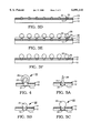
- FIGS. 1A to 1E are views showing the continued steps of forming a plurality of chip bumps of a bump chip scale semiconductor package in accordance with the primary embodiment of the present invention
- FIGS. 2A and 2B are views showing the steps of positioning solder balls, being substituted for the step of FIG. 1D, in accordance with second and third embodiments, respectively;
- FIGS. 3A to 3F are views showing the continued steps of forming a plurality of chip bumps of a bump chip scale semiconductor package in accordance with the fourth embodiment of the present invention.
- FIG. 4 is a sectional view of a chip bump formed in accordance with each of the chip bump forming methods of the primary to third embodiments of this invention.
- FIGS. 5A to 5C are sectional views showing a method of forming a chip bump in accordance with another example of the fourth embodiment of this invention.
- FIG. 6 is a view showing a method of forming a plurality of bumps on the unit semiconductor chips of a wafer at the same time prior to cutting the wafer into the unit semiconductor chips in accordance with the present invention
- FIGS. 7A and 7B are views showing the continued steps of mounting the bump chip scale semiconductor package of this invention to a mother board;
- FIG. 8 is a sectional view showing the construction of a bump chip scale semiconductor package covered with a lid in accordance with a further embodiment of the present invention.
- FIG. 9 is a sectional view showing the construction of a typical BGA (ball grid array) semiconductor package.
- FIGS. 1A to 1E are views showing the continued steps of forming a plurality of chip bumps of a bump chip scale semiconductor package in accordance with the primary embodiment of the present invention.
- the solder or gold wires used in this invention may be selected from solder or gold wires which have been typically used in the wire bonding step of a conventional package producing process.
- FIG. 1A is a side sectional view showing the step of forming a plurality of gold bumps 21, each of which has a straight gold tail 22 on one end thereof, on the chip pads 11, which are formed on one side of a semiconductor chip 10, using a plurality of gold wires.
- a passivation thin film 12 which is not chemically reactive but is electrically insulated, is formed on the semiconductor chip 10 except therefor the chip pads 11.
- Such a passivation thin film 12 may be formed from glass or polyimide.
- FIG. 1B is a side sectional view showing the step of forming a resin coating layer 13 by applying a resin layer of a uniform thickness onto the passivation thin film 12 of the chip around the solder bump leaving a part of each solder tail extending from the resin layer as clearly seen in FIG. 1B, 10 and by heating and curing the resin layer at a high temperature of about 150-240° C. for at least 30 minutes.
- the resin may be selected from a high insulating resin such as a polyimide or epoxy resin.
- FIG. 1C is a side sectional view showing the step of forming bent gold tails 23 by bending the exposed parts of the straight gold tails 22 using a coining machine 50 after curing the resin coating layer 13. In this step, the exposed parts of the gold tails 22 are exposed outside the cured layer 13.
- FIG. 1D is a side sectional view showing the step of positioning a plurality of Sn/Pb base solder balls 28 on the bent gold tails 23.
- a flux 35 is applied to the bent gold tails 23 prior to positioning the solder balls 28, which have been previously formed into a desirable size, on the bent gold tails 23.
- the flux 35 may be selected from a resin, organic or inorganic base flux. However, it is preferable to use a rosin base flux, which is a kind of resin base flux, as the flux 35.
- FIG. 1E is a side sectional view showing the step of reforming a plurality of chip bumps 20.
- the semiconductor chip 10 from the solder ball positioning step is treated by a convection oven, furnace or IR (infrared ray) reflow device maintaining a high temperature higher than 190° C. thus reforming the chip bumps 20 each of which has a spherical or hemispherical configuration with a core being formed from each bent gold tail 23.
- IR infrared ray
- FIGS. 2A and 2B are views showing the steps of positioning the solder balls, substituting for the step of FIG. 1D, in accordance with second and third embodiments, respectively.
- FIG. 2A is a side view showing the step of applying a solder paste 27 on the resin coating layer 13 of the chip 10 at a position including each bent gold tail 23.
- a sufficient amount of solder paste 27 to form a desirable-sized chip bump is applied to the resin coating layer 13 at a position including each bent gold tail 23 through a stencil or screen printing process.
- a flux may be used.
- the other steps except for the solder ball positioning step remain the same as described for the primary embodiment.
- FIG. 2B is a side view showing the step of forming a solder bump on each bent gold tail 23.
- a flux preferably a rosin base flux 35 is applied to the resin coating layer 13 thus covering the bent gold tails 23.
- the chip 10 in turn is turned over with the bent gold tails 23 being directed downward. Thereafter, the bent gold tails 23 are immersed into a solder pot 60 thus forming the solder bumps on the respective bent gold tails 23.
- the other steps except for the solder ball positioning step remain the same as described for the primary embodiment.
- solder bumps of this invention may be formed on the bent gold tails 23 by a wave soldering process in place of immersing the bent gold tails 23 into the solder pot 60.
- the chip bumps 20 may be directly formed on a wafer 70 as shown in FIG. 6 in place of forming the chip bumps 30 on a unit semiconductor chip.
- the wafer 70 is cut into a plurality of unit semiconductor chips using a sawing machine prior to producing a unit bump chip scale semiconductor package 100 as shown in FIG. 7A. In this case, it is possible to remarkably improve work efficiency while producing the bump chip scale semiconductor packages.
- the bent gold tails 23 are formed from gold wires which are cheap and have a high conductivity in comparison with expensive solder wires. Thereafter, the chip bumps 20 are simply and effectively formed using the bent gold tails 23 as the cores of the chip bumps 20.
- the chip bumps 20 are used as the signal input and output terminals of the package and are used as surface mounting joints when the chip 10 is mounted on the mother board. Therefore, the method of this invention provides a compact, small, lightened and thinned bump chip scale semiconductor package.
- FIGS. 3A to 3F are views showing the continued steps of forming the chip bumps of a bump chip scale semiconductor package in accordance with the fourth embodiment of the this invention.
- the solder tails 26 of a plurality of solder bumps 25 are directly fused by a heat treating means prior to cooling the fused solder bumps 25, thus forming the chip bumps 20 having a different structure from the primary to third embodiments in which the bent gold tails 23 are used as the cores of the chip bumps 20.
- FIG. 3A is a side sectional view showing a semiconductor chip 10 having a passivation thin film 12 which is formed on the chip 10 except at the chip pads 11.
- the detailed description of the step of FIG. 3A may be understood by referring to the description of the step of FIG. 1A.
- FIG. 3B is a side sectional view showing the step of forming a plurality of solder bumps 25.
- each of the bumps 25 has a straight solder tail 26 on one end thereof and is formed on each chip pad 11 of the chip 10 using a solder wire from a ball bonding wire bonder.
- each of the straight solder tails 26, which is to be formed into a chip bump having an appropriate diameter has a height of 5-40 mil, preferably 10-30 mil.
- FIG. 3C is a side sectional view showing the step of forming a resin coating layer 13 by applying a resin layer of a uniform thickness onto the passivation thin film 12 of the chip 10 having the solder bumps 25 and by heating and curing the resin layer at a high temperature of about 150-240° C. for at least 30 minutes.
- the detailed description of the step of FIG. 3C may be understood by referring to the description of the step of FIG. 1B.
- FIG. 3D is a side sectional view showing the step of forming the chip bumps 20.
- the solder tails 26 are fused using a heat treating means prior to cooling the fused tails 26. While cooling the fused tails 26, the fused tails 26 are formed into spherical or hemispherical chip bumps 20 due to gravity and surface tension.
- the heat treating means and temperature conditions used in this step may be understood by referring to those of the step of the primary to third embodiments of this invention.
- a flux 35 preferably a rosin base flux may be applied to the resin coating layer 13 prior to forming the chip bumps 20.
- FIGS. 3E and 3F show a method of enlarging the diameter of each chip bump 20 as desired.
- a rosin base flux 35 is applied to the resin coating layer 13.
- a solder paste applying step or a solder ball positioning step is performed.
- the solder paste applying step a sufficient amount of solder paste 27 to form a desirable-sized chip bump is applied to each existing chip bump 20.
- a previously-formed solder ball 28 having a diameter sufficient to form a desirable-sized chip bump is positioned on each existing chip bump 20.
- the chip 10 is treated by a heat treating means such as an oven or furnace thus reforming the chip bumps 20 and enlarging the diameters of the chip bumps 20.
- FIG. 4 is a sectional view of a chip bump 20 which is formed in accordance with each of the chip bump forming methods of the primary to third embodiments of this invention.
- the chip bump 20 which is used as a signal input or output terminal of the package and is used as a surface mounting to joint when the chip 10 is mounted a mother board, comprises a hemispherical gold bump 21, an arcuate gold tail 23 integrally extending from the top of the gold bump 21 and a spherical or hemispherical solder bump 25 formed on the gold bump 21 with the arcuate gold tail 23 being used as the core of the solder bump 25.
- the gold tail 23 has a length of 5-40 mil, preferably 10-30 mil.
- FIGS. 5A to 5C are sectional views showing a method of forming a chip bump in accordance with another example of the fourth embodiment of this invention.
- the chip bumps 20 of this invention may be formed by the following steps in place of directly forming the chip bumps 20 on the chip pads 11. That is, a gold bump 24 free from a gold tail is formed on each chip pad 11 of a semiconductor chip 10 using a gold wire. After the gold bump forming step, a solder bump 25 having a solder tail 26 is formed on the core of the gold bump 24 using a solder wire as shown in FIG. 5A. Thereafter, the same chip bump forming step as that of the fourth embodiment of this invention is performed thus forming the chip bump 20 as shown in FIG. 5B.
- the chip bump 20 comprises a hemispherical gold bump core 24 and a spherical or hemispherical solder bump 25 formed on the top of the gold bump core 24 while surrounding the gold bump core 24 as shown in FIG. 5C.
- the chip bumps 20 of this invention may be directly formed on a plurality of semiconductor chips of a wafer 70 at the same time.
- the wafer 70 is cut into a plurality of unit semiconductor chips using a sawing machine prior to producing a unit bump chip scale semiconductor package 100. In this case, it is possible to remarkably improve work efficiency while producing the bump chip scale semiconductor packages.
- FIGS. 7A and 7B are views showing the continued steps of turning over a bump chip scale semiconductor package 100 of this invention and of mounting the package 100 to a mother board 40.
- the bump chip scale semiconductor package 100 produced in accordance with the present invention comprises a semiconductor chip 10.
- the chip 10 has a plurality of chip pads 11, used as conductive electrodes, and a passivation thin film 12 formed on one side of the chip 10 except at the chip pads 11.
- the package 100 also includes a plurality of chip bumps 20, which are used as signal input and output terminals of the package relative to a mother board and are used as joints for mounting the semiconductor chip 10 to the mother board.
- Each chip bump 20 comprises a gold bump core, which is welded to each chip pad 11, and a solder bump which covers the gold bump core.
- a resin coating layer 13 is layered on the passivation thin film 12 and surrounds the lower portions of the chip bumps 20.
- Each gold bump core may be a core with an arcuate gold tail. In this case, the gold tail has a length of 5-40 mil, preferably 10-30 mil. Alternatively, each gold bump core may be a tailless core.
- FIG. 8 is a sectional view showing the construction of a bump chip scale semiconductor package 100 covered with a lid 30 in accordance with a further embodiment of the present invention.
- the lid 30 covers the five surfaces of the hexahedral semiconductor chip 10 except for the surface having the chip bumps 20 thus protecting the chip 10 from the atmospheric environment.
- the above lid 30 is formed from a high thermal conductive metal or plastic such as epoxy.
- the thermal conductive metal of the lid 30 may be selected from the group of copper, copper alloys, steels and stainless steels.
- a metal lid 30 may be preferably plated with nickel.
- the lid 30 In order to attach the lid 30 to the chip 10, the lid 30 is primarily attached to the chip 10 with an epoxy base resin 31 being applied to the internal surface of the lid 30. Thereafter, the lid 30 and chip 10 are heated at a high temperature higher than 100° C. thus completely curing the resin 31. The junction between the chip 10 and the metal or plastic lid 30 is tightly filled with epoxy base resin without any void remaining in the junction.
- the present invention provides a method of forming chip bumps of a bump chip scale semiconductor package.
- the method easily and effectively forms the chip bumps of the package at a low cost.
- the chip bumps are directly formed on the chip pads of a semiconductor chip.
- the above chip bumps are used as the signal input and output terminals of the package and are used as surface mounting joints when the chip is mounted to a mother board. Therefore, the method of this invention provides a compact, small, lightened and thinned bump chip scale semiconductor package.
Abstract
Description
Claims (20)
Priority Applications (1)
| Application Number | Priority Date | Filing Date | Title |
|---|---|---|---|
| US09/222,226 US6091141A (en) | 1996-03-11 | 1998-12-29 | Bump chip scale semiconductor package |
Applications Claiming Priority (6)
| Application Number | Priority Date | Filing Date | Title |
|---|---|---|---|
| KR96-06302 | 1996-03-11 | ||
| KR96-06303 | 1996-03-11 | ||
| KR1019960006302A KR100192758B1 (en) | 1996-03-11 | 1996-03-11 | Method of manufacturing semiconductor package and structure of the same |
| KR1019960006303A KR100192759B1 (en) | 1996-03-11 | 1996-03-11 | Method of manufacturing bump for bump chip scale package |
| US08/813,725 US5908317A (en) | 1996-03-11 | 1997-03-07 | Method of forming chip bumps of bump chip scale semiconductor package |
| US09/222,226 US6091141A (en) | 1996-03-11 | 1998-12-29 | Bump chip scale semiconductor package |
Related Parent Applications (1)
| Application Number | Title | Priority Date | Filing Date |
|---|---|---|---|
| US08/813,725 Division US5908317A (en) | 1996-03-11 | 1997-03-07 | Method of forming chip bumps of bump chip scale semiconductor package |
Publications (1)
| Publication Number | Publication Date |
|---|---|
| US6091141A true US6091141A (en) | 2000-07-18 |
Family
ID=26631674
Family Applications (2)
| Application Number | Title | Priority Date | Filing Date |
|---|---|---|---|
| US08/813,725 Expired - Lifetime US5908317A (en) | 1996-03-11 | 1997-03-07 | Method of forming chip bumps of bump chip scale semiconductor package |
| US09/222,226 Expired - Lifetime US6091141A (en) | 1996-03-11 | 1998-12-29 | Bump chip scale semiconductor package |
Family Applications Before (1)
| Application Number | Title | Priority Date | Filing Date |
|---|---|---|---|
| US08/813,725 Expired - Lifetime US5908317A (en) | 1996-03-11 | 1997-03-07 | Method of forming chip bumps of bump chip scale semiconductor package |
Country Status (2)
| Country | Link |
|---|---|
| US (2) | US5908317A (en) |
| JP (1) | JP3146345B2 (en) |
Cited By (21)
| Publication number | Priority date | Publication date | Assignee | Title |
|---|---|---|---|---|
| US6177731B1 (en) * | 1998-01-19 | 2001-01-23 | Citizen Watch Co., Ltd. | Semiconductor package |
| US6365977B1 (en) * | 1999-08-31 | 2002-04-02 | International Business Machines Corporation | Insulating interposer between two electronic components and process thereof |
| US6372624B1 (en) * | 1997-08-04 | 2002-04-16 | Micron Technology, Inc. | Method for fabricating solder bumps by wave soldering |
| US20030071363A1 (en) * | 2001-10-11 | 2003-04-17 | Hideaki Yoshida | Semiconductor device |
| US20040000714A1 (en) * | 2002-06-27 | 2004-01-01 | Umc Japan | Semiconductor device and manufacturing method therefor |
| US6803303B1 (en) | 2002-07-11 | 2004-10-12 | Micron Technology, Inc. | Method of fabricating semiconductor component having encapsulated, bonded, interconnect contacts |
| US6841874B1 (en) | 2002-11-01 | 2005-01-11 | Amkor Technology, Inc. | Wafer-level chip-scale package |
| US20050148111A1 (en) * | 2003-12-30 | 2005-07-07 | Texas Instruments Incorporated | Method and system for producing resilient solder joints |
| US20060216868A1 (en) * | 2005-03-25 | 2006-09-28 | Advanced Semiconductor Engineering Inc. | Package structure and fabrication thereof |
| EP2154258A1 (en) | 2008-08-06 | 2010-02-17 | General Electric Company | Nickel-base superalloy, unidirectional-solidification process therefor, and castings formed therefrom |
| US20100071812A1 (en) * | 2008-09-25 | 2010-03-25 | General Electric Company | Unidirectionally-solidification process and castings formed thereby |
| US8008130B2 (en) * | 1999-10-05 | 2011-08-30 | Renesas Electronics Corporation | Multilayer interconnection board, semiconductor device having the same, and method of forming the same as well as method of mounting the semicondutor chip on the interconnection board |
| US20120086123A1 (en) * | 2010-10-06 | 2012-04-12 | Samsung Electronics Co., Ltd. | Semiconductor assembly and semiconductor package including a solder channel |
| US20130167369A1 (en) * | 2012-01-02 | 2013-07-04 | Samsung Electronics Co., Ltd. | Apparatuses for mounting semiconductor chips |
| US20140187034A1 (en) * | 2009-12-10 | 2014-07-03 | International Business Machines Corporation | Integrated circuit chip with pyramid or cone-shaped conductive pads for flexible c4 connections and a method of forming the integrated circuit chip |
| US9105530B2 (en) | 2012-09-18 | 2015-08-11 | Taiwan Semiconductor Manufacturing Company, Ltd. | Conductive contacts having varying widths and method of manufacturing same |
| US9142533B2 (en) | 2010-05-20 | 2015-09-22 | Taiwan Semiconductor Manufacturing Company, Ltd. | Substrate interconnections having different sizes |
| US9299674B2 (en) | 2012-04-18 | 2016-03-29 | Taiwan Semiconductor Manufacturing Company, Ltd. | Bump-on-trace interconnect |
| US9425136B2 (en) * | 2012-04-17 | 2016-08-23 | Taiwan Semiconductor Manufacturing Company, Ltd. | Conical-shaped or tier-shaped pillar connections |
| US9646923B2 (en) | 2012-04-17 | 2017-05-09 | Taiwan Semiconductor Manufacturing Company, Ltd. | Semiconductor devices, methods of manufacture thereof, and packaged semiconductor devices |
| US11669281B1 (en) * | 2021-11-19 | 2023-06-06 | Meta Platforms, Inc. | Count circuit for symbol statistics |
Families Citing this family (55)
| Publication number | Priority date | Publication date | Assignee | Title |
|---|---|---|---|---|
| US6413797B2 (en) * | 1997-10-09 | 2002-07-02 | Rohm Co., Ltd. | Semiconductor device and method for making the same |
| JP4239310B2 (en) * | 1998-09-01 | 2009-03-18 | ソニー株式会社 | Manufacturing method of semiconductor device |
| US6930390B2 (en) * | 1999-01-20 | 2005-08-16 | Sony Chemicals Corp. | Flexible printed wiring boards |
| US6255208B1 (en) * | 1999-01-25 | 2001-07-03 | International Business Machines Corporation | Selective wafer-level testing and burn-in |
| JP3346320B2 (en) * | 1999-02-03 | 2002-11-18 | カシオ計算機株式会社 | Semiconductor device and manufacturing method thereof |
| US6177726B1 (en) * | 1999-02-11 | 2001-01-23 | Philips Electronics North America Corporation | SiO2 wire bond insulation in semiconductor assemblies |
| JP3223283B2 (en) * | 1999-09-14 | 2001-10-29 | カシオ計算機株式会社 | Method for manufacturing semiconductor device |
| KR20010028754A (en) * | 1999-09-22 | 2001-04-06 | 김영환 | Process for chip size package enhanced solder joint |
| JP3672297B2 (en) * | 1999-11-10 | 2005-07-20 | セイコーインスツル株式会社 | Manufacturing method of semiconductor device |
| US6717245B1 (en) * | 2000-06-02 | 2004-04-06 | Micron Technology, Inc. | Chip scale packages performed by wafer level processing |
| JP3420203B2 (en) * | 2000-10-27 | 2003-06-23 | Necエレクトロニクス株式会社 | Solder bump formation method |
| TW465064B (en) * | 2000-12-22 | 2001-11-21 | Advanced Semiconductor Eng | Bonding process and the structure thereof |
| SG99877A1 (en) * | 2001-01-04 | 2003-11-27 | Inst Materials Research & Eng | Forming an electrical contact on an electronic component |
| US7115998B2 (en) * | 2002-08-29 | 2006-10-03 | Micron Technology, Inc. | Multi-component integrated circuit contacts |
| US7271497B2 (en) * | 2003-03-10 | 2007-09-18 | Fairchild Semiconductor Corporation | Dual metal stud bumping for flip chip applications |
| US6815836B2 (en) * | 2003-03-24 | 2004-11-09 | Texas Instruments Incorporated | Wire bonding for thin semiconductor package |
| DE10318074B4 (en) * | 2003-04-17 | 2009-05-20 | Qimonda Ag | Process for making BOC module assemblies with improved mechanical properties |
| US20050133933A1 (en) * | 2003-12-19 | 2005-06-23 | Advanpack Solutions Pte. Ltd. | Various structure/height bumps for wafer level-chip scale package |
| KR100648039B1 (en) * | 2004-09-13 | 2006-11-23 | 삼성전자주식회사 | method of forming solder ball and related fabrication and structure of semiconductor package using the method |
| US8525314B2 (en) | 2004-11-03 | 2013-09-03 | Tessera, Inc. | Stacked packaging improvements |
| TWI284949B (en) * | 2005-09-09 | 2007-08-01 | Chipmos Technologies Inc | Bumped structure and its forming method |
| US8058101B2 (en) | 2005-12-23 | 2011-11-15 | Tessera, Inc. | Microelectronic packages and methods therefor |
| MY149251A (en) * | 2008-10-23 | 2013-07-31 | Carsem M Sdn Bhd | Wafer-level package using stud bump coated with solder |
| US8482111B2 (en) | 2010-07-19 | 2013-07-09 | Tessera, Inc. | Stackable molded microelectronic packages |
| KR101128063B1 (en) | 2011-05-03 | 2012-04-23 | 테세라, 인코포레이티드 | Package-on-package assembly with wire bonds to encapsulation surface |
| US9105483B2 (en) | 2011-10-17 | 2015-08-11 | Invensas Corporation | Package-on-package assembly with wire bond vias |
| US8946757B2 (en) | 2012-02-17 | 2015-02-03 | Invensas Corporation | Heat spreading substrate with embedded interconnects |
| US8372741B1 (en) * | 2012-02-24 | 2013-02-12 | Invensas Corporation | Method for package-on-package assembly with wire bonds to encapsulation surface |
| US8835228B2 (en) | 2012-05-22 | 2014-09-16 | Invensas Corporation | Substrate-less stackable package with wire-bond interconnect |
| US9171790B2 (en) * | 2012-05-30 | 2015-10-27 | Taiwan Semiconductor Manufacturing Company, Ltd. | Package on package devices and methods of packaging semiconductor dies |
| US9391008B2 (en) | 2012-07-31 | 2016-07-12 | Invensas Corporation | Reconstituted wafer-level package DRAM |
| US9502390B2 (en) | 2012-08-03 | 2016-11-22 | Invensas Corporation | BVA interposer |
| US8878353B2 (en) | 2012-12-20 | 2014-11-04 | Invensas Corporation | Structure for microelectronic packaging with bond elements to encapsulation surface |
| US9136254B2 (en) | 2013-02-01 | 2015-09-15 | Invensas Corporation | Microelectronic package having wire bond vias and stiffening layer |
| US9167710B2 (en) | 2013-08-07 | 2015-10-20 | Invensas Corporation | Embedded packaging with preformed vias |
| US9685365B2 (en) | 2013-08-08 | 2017-06-20 | Invensas Corporation | Method of forming a wire bond having a free end |
| US20150076714A1 (en) | 2013-09-16 | 2015-03-19 | Invensas Corporation | Microelectronic element with bond elements to encapsulation surface |
| US9263394B2 (en) | 2013-11-22 | 2016-02-16 | Invensas Corporation | Multiple bond via arrays of different wire heights on a same substrate |
| US9583456B2 (en) | 2013-11-22 | 2017-02-28 | Invensas Corporation | Multiple bond via arrays of different wire heights on a same substrate |
| US9379074B2 (en) | 2013-11-22 | 2016-06-28 | Invensas Corporation | Die stacks with one or more bond via arrays of wire bond wires and with one or more arrays of bump interconnects |
| US9583411B2 (en) | 2014-01-17 | 2017-02-28 | Invensas Corporation | Fine pitch BVA using reconstituted wafer with area array accessible for testing |
| US10381326B2 (en) | 2014-05-28 | 2019-08-13 | Invensas Corporation | Structure and method for integrated circuits packaging with increased density |
| US9735084B2 (en) | 2014-12-11 | 2017-08-15 | Invensas Corporation | Bond via array for thermal conductivity |
| US9888579B2 (en) | 2015-03-05 | 2018-02-06 | Invensas Corporation | Pressing of wire bond wire tips to provide bent-over tips |
| US9502372B1 (en) | 2015-04-30 | 2016-11-22 | Invensas Corporation | Wafer-level packaging using wire bond wires in place of a redistribution layer |
| US9761554B2 (en) | 2015-05-07 | 2017-09-12 | Invensas Corporation | Ball bonding metal wire bond wires to metal pads |
| US9490222B1 (en) | 2015-10-12 | 2016-11-08 | Invensas Corporation | Wire bond wires for interference shielding |
| US10490528B2 (en) | 2015-10-12 | 2019-11-26 | Invensas Corporation | Embedded wire bond wires |
| US10332854B2 (en) | 2015-10-23 | 2019-06-25 | Invensas Corporation | Anchoring structure of fine pitch bva |
| US10181457B2 (en) | 2015-10-26 | 2019-01-15 | Invensas Corporation | Microelectronic package for wafer-level chip scale packaging with fan-out |
| US9911718B2 (en) | 2015-11-17 | 2018-03-06 | Invensas Corporation | ‘RDL-First’ packaged microelectronic device for a package-on-package device |
| US9659848B1 (en) | 2015-11-18 | 2017-05-23 | Invensas Corporation | Stiffened wires for offset BVA |
| US9984992B2 (en) | 2015-12-30 | 2018-05-29 | Invensas Corporation | Embedded wire bond wires for vertical integration with separate surface mount and wire bond mounting surfaces |
| US9935075B2 (en) | 2016-07-29 | 2018-04-03 | Invensas Corporation | Wire bonding method and apparatus for electromagnetic interference shielding |
| US10299368B2 (en) | 2016-12-21 | 2019-05-21 | Invensas Corporation | Surface integrated waveguides and circuit structures therefor |
Citations (3)
| Publication number | Priority date | Publication date | Assignee | Title |
|---|---|---|---|---|
| US5391397A (en) * | 1994-04-05 | 1995-02-21 | Motorola, Inc. | Method of adhesion to a polyimide surface by formation of covalent bonds |
| US5585671A (en) * | 1994-10-07 | 1996-12-17 | Nagesh; Voddarahalli K. | Reliable low thermal resistance package for high power flip clip ICs |
| US5813115A (en) * | 1994-08-03 | 1998-09-29 | Matsushita Electric Industrial Co., Ltd. | Method of mounting a semiconductor chip on a wiring substrate |
Family Cites Families (19)
| Publication number | Priority date | Publication date | Assignee | Title |
|---|---|---|---|---|
| US4067104A (en) * | 1977-02-24 | 1978-01-10 | Rockwell International Corporation | Method of fabricating an array of flexible metallic interconnects for coupling microelectronics components |
| US4661192A (en) * | 1985-08-22 | 1987-04-28 | Motorola, Inc. | Low cost integrated circuit bonding process |
| JPS63114138A (en) * | 1986-10-31 | 1988-05-19 | Hitachi Ltd | Bonding method for wire laminated layer |
| US4752027A (en) * | 1987-02-20 | 1988-06-21 | Hewlett-Packard Company | Method and apparatus for solder bumping of printed circuit boards |
| US5014111A (en) * | 1987-12-08 | 1991-05-07 | Matsushita Electric Industrial Co., Ltd. | Electrical contact bump and a package provided with the same |
| US5071787A (en) * | 1989-03-14 | 1991-12-10 | Kabushiki Kaisha Toshiba | Semiconductor device utilizing a face-down bonding and a method for manufacturing the same |
| US5060843A (en) * | 1989-06-07 | 1991-10-29 | Nec Corporation | Process of forming bump on electrode of semiconductor chip and apparatus used therefor |
| JPH0350736A (en) * | 1989-07-18 | 1991-03-05 | Nec Corp | Manufacture of bump of semiconductor chip |
| US5504035A (en) * | 1989-08-28 | 1996-04-02 | Lsi Logic Corporation | Process for solder ball interconnecting a semiconductor device to a substrate using a noble metal foil embedded interposer substrate |
| JP2836027B2 (en) * | 1989-12-18 | 1998-12-14 | カシオ計算機株式会社 | Method of forming solder bumps |
| KR940001149B1 (en) * | 1991-04-16 | 1994-02-14 | 삼성전자 주식회사 | Chip bonding method of semiconductor device |
| US5496775A (en) * | 1992-07-15 | 1996-03-05 | Micron Semiconductor, Inc. | Semiconductor device having ball-bonded pads |
| US5455461A (en) * | 1992-09-21 | 1995-10-03 | Fujitsu Limited | Semiconductor device having reformed pad |
| US5485949A (en) * | 1993-04-30 | 1996-01-23 | Matsushita Electric Industrial Co., Ltd. | Capillary for a wire bonding apparatus and a method for forming an electric connection bump using the capillary |
| US5508561A (en) * | 1993-11-15 | 1996-04-16 | Nec Corporation | Apparatus for forming a double-bump structure used for flip-chip mounting |
| JPH0817860A (en) * | 1994-06-30 | 1996-01-19 | Oki Electric Ind Co Ltd | Manufacture of electronic part |
| US5579573A (en) * | 1994-10-11 | 1996-12-03 | Ford Motor Company | Method for fabricating an undercoated chip electrically interconnected to a substrate |
| US5492863A (en) * | 1994-10-19 | 1996-02-20 | Motorola, Inc. | Method for forming conductive bumps on a semiconductor device |
| US5650667A (en) * | 1995-10-30 | 1997-07-22 | National Semiconductor Corporation | Process of forming conductive bumps on the electrodes of semiconductor chips using lapping and the bumps thereby created |
-
1997
- 1997-01-22 JP JP02314497A patent/JP3146345B2/en not_active Expired - Fee Related
- 1997-03-07 US US08/813,725 patent/US5908317A/en not_active Expired - Lifetime
-
1998
- 1998-12-29 US US09/222,226 patent/US6091141A/en not_active Expired - Lifetime
Patent Citations (3)
| Publication number | Priority date | Publication date | Assignee | Title |
|---|---|---|---|---|
| US5391397A (en) * | 1994-04-05 | 1995-02-21 | Motorola, Inc. | Method of adhesion to a polyimide surface by formation of covalent bonds |
| US5813115A (en) * | 1994-08-03 | 1998-09-29 | Matsushita Electric Industrial Co., Ltd. | Method of mounting a semiconductor chip on a wiring substrate |
| US5585671A (en) * | 1994-10-07 | 1996-12-17 | Nagesh; Voddarahalli K. | Reliable low thermal resistance package for high power flip clip ICs |
Cited By (51)
| Publication number | Priority date | Publication date | Assignee | Title |
|---|---|---|---|---|
| US6372624B1 (en) * | 1997-08-04 | 2002-04-16 | Micron Technology, Inc. | Method for fabricating solder bumps by wave soldering |
| US6637638B1 (en) | 1997-08-04 | 2003-10-28 | Micron Technology, Inc. | System for fabricating solder bumps on semiconductor components |
| US6177731B1 (en) * | 1998-01-19 | 2001-01-23 | Citizen Watch Co., Ltd. | Semiconductor package |
| US6365977B1 (en) * | 1999-08-31 | 2002-04-02 | International Business Machines Corporation | Insulating interposer between two electronic components and process thereof |
| US8008130B2 (en) * | 1999-10-05 | 2011-08-30 | Renesas Electronics Corporation | Multilayer interconnection board, semiconductor device having the same, and method of forming the same as well as method of mounting the semicondutor chip on the interconnection board |
| US20030071363A1 (en) * | 2001-10-11 | 2003-04-17 | Hideaki Yoshida | Semiconductor device |
| US6841873B2 (en) * | 2001-10-11 | 2005-01-11 | Oki Electric Industry Co., Ltd. | CSP Semiconductor device having signal and radiation bump groups |
| US20050035469A1 (en) * | 2001-10-11 | 2005-02-17 | Hideaki Yoshida | CSP semiconductor device having signal and radiation bump groups |
| US7253520B2 (en) | 2001-10-11 | 2007-08-07 | Oki Electric Industry Co., Ltd. | CSP semiconductor device having signal and radiation bump groups |
| US6894389B2 (en) * | 2002-06-27 | 2005-05-17 | Umc Japan | Semiconductor device and manufacturing method therefor |
| US20040000714A1 (en) * | 2002-06-27 | 2004-01-01 | Umc Japan | Semiconductor device and manufacturing method therefor |
| US6803303B1 (en) | 2002-07-11 | 2004-10-12 | Micron Technology, Inc. | Method of fabricating semiconductor component having encapsulated, bonded, interconnect contacts |
| US6906418B2 (en) | 2002-07-11 | 2005-06-14 | Micron Technology, Inc. | Semiconductor component having encapsulated, bonded, interconnect contacts |
| US7129573B2 (en) | 2002-07-11 | 2006-10-31 | Micron Technology, Inc. | System having semiconductor component with encapsulated, bonded, interconnect contacts |
| US20070048998A1 (en) * | 2002-07-11 | 2007-03-01 | Hiatt William M | Method for fabricating semiconductor components encapsulated, bonded, interconnect contacts on redistribution contacts |
| US20050064695A1 (en) * | 2002-07-11 | 2005-03-24 | Hiatt William M. | System having semiconductor component with encapsulated, bonded, interconnect contacts |
| US7256116B2 (en) | 2002-07-11 | 2007-08-14 | Micron Technology, Inc. | Method for fabricating semiconductor components having encapsulated, bonded, interconnect contacts on redistribution contacts |
| US6841874B1 (en) | 2002-11-01 | 2005-01-11 | Amkor Technology, Inc. | Wafer-level chip-scale package |
| US6987319B1 (en) | 2002-11-01 | 2006-01-17 | Amkor Technology, Inc. | Wafer-level chip-scale package |
| US20050148111A1 (en) * | 2003-12-30 | 2005-07-07 | Texas Instruments Incorporated | Method and system for producing resilient solder joints |
| US20060216868A1 (en) * | 2005-03-25 | 2006-09-28 | Advanced Semiconductor Engineering Inc. | Package structure and fabrication thereof |
| EP2154258A1 (en) | 2008-08-06 | 2010-02-17 | General Electric Company | Nickel-base superalloy, unidirectional-solidification process therefor, and castings formed therefrom |
| US20100071812A1 (en) * | 2008-09-25 | 2010-03-25 | General Electric Company | Unidirectionally-solidification process and castings formed thereby |
| US9269683B2 (en) * | 2009-12-10 | 2016-02-23 | Globalfoundries Inc. | Integrated circuit chip with pyramid or cone-shaped conductive pads for flexible C4 connections and a method of forming the integrated circuit chip |
| US20140187034A1 (en) * | 2009-12-10 | 2014-07-03 | International Business Machines Corporation | Integrated circuit chip with pyramid or cone-shaped conductive pads for flexible c4 connections and a method of forming the integrated circuit chip |
| US9773755B2 (en) | 2010-05-20 | 2017-09-26 | Taiwan Semiconductor Manufacturing Company, Ltd. | Substrate interconnections having different sizes |
| US9142533B2 (en) | 2010-05-20 | 2015-09-22 | Taiwan Semiconductor Manufacturing Company, Ltd. | Substrate interconnections having different sizes |
| US8710657B2 (en) * | 2010-10-06 | 2014-04-29 | Samsung Electronics Co., Ltd. | Semiconductor assembly and semiconductor package including a solder channel |
| US20120086123A1 (en) * | 2010-10-06 | 2012-04-12 | Samsung Electronics Co., Ltd. | Semiconductor assembly and semiconductor package including a solder channel |
| US20130167369A1 (en) * | 2012-01-02 | 2013-07-04 | Samsung Electronics Co., Ltd. | Apparatuses for mounting semiconductor chips |
| US10056345B2 (en) | 2012-04-17 | 2018-08-21 | Taiwan Semiconductor Manufacturing Company, Ltd. | Conical-shaped or tier-shaped pillar connections |
| US9425136B2 (en) * | 2012-04-17 | 2016-08-23 | Taiwan Semiconductor Manufacturing Company, Ltd. | Conical-shaped or tier-shaped pillar connections |
| US11315896B2 (en) | 2012-04-17 | 2022-04-26 | Taiwan Semiconductor Manufacturing Company, Ltd. | Conical-shaped or tier-shaped pillar connections |
| US9646923B2 (en) | 2012-04-17 | 2017-05-09 | Taiwan Semiconductor Manufacturing Company, Ltd. | Semiconductor devices, methods of manufacture thereof, and packaged semiconductor devices |
| US10153243B2 (en) | 2012-04-17 | 2018-12-11 | Taiwan Semiconductor Manufacturing Company, Ltd. | Semiconductor devices, methods of manufacture thereof, and packaged semiconductor devices |
| US11682651B2 (en) | 2012-04-18 | 2023-06-20 | Taiwan Semiconductor Manufacturing Company | Bump-on-trace interconnect |
| US9299674B2 (en) | 2012-04-18 | 2016-03-29 | Taiwan Semiconductor Manufacturing Company, Ltd. | Bump-on-trace interconnect |
| US10847493B2 (en) | 2012-04-18 | 2020-11-24 | Taiwan Semiconductor Manufacturing, Ltd. | Bump-on-trace interconnect |
| US10510710B2 (en) | 2012-04-18 | 2019-12-17 | Taiwan Semiconductor Manufacturing Company, Ltd. | Bump-on-trace interconnect |
| US9991224B2 (en) | 2012-04-18 | 2018-06-05 | Taiwan Semiconductor Manufacturing Company, Ltd. | Bump-on-trace interconnect having varying widths and methods of forming same |
| US9966346B2 (en) | 2012-09-18 | 2018-05-08 | Taiwan Semiconductor Manufacturing Company | Bump structure and method of forming same |
| US10008459B2 (en) | 2012-09-18 | 2018-06-26 | Taiwan Semiconductor Manufacturing Company | Structures having a tapering curved profile and methods of making same |
| US9111817B2 (en) | 2012-09-18 | 2015-08-18 | Taiwan Semiconductor Manufacturing Company, Ltd. | Bump structure and method of forming same |
| US10319691B2 (en) | 2012-09-18 | 2019-06-11 | Taiwan Semiconductor Manufacturing Company | Solderless interconnection structure and method of forming same |
| US9953939B2 (en) | 2012-09-18 | 2018-04-24 | Taiwan Semiconductor Manufacturing Company, Ltd. | Conductive contacts having varying widths and method of manufacturing same |
| US9508668B2 (en) | 2012-09-18 | 2016-11-29 | Taiwan Semiconductor Manufacturing Company, Ltd. | Conductive contacts having varying widths and method of manufacturing same |
| US11043462B2 (en) | 2012-09-18 | 2021-06-22 | Taiwan Semiconductor Manufacturing Company | Solderless interconnection structure and method of forming same |
| US9496233B2 (en) | 2012-09-18 | 2016-11-15 | Taiwan Semiconductor Manufacturing Company, Ltd. | Interconnection structure and method of forming same |
| US9105530B2 (en) | 2012-09-18 | 2015-08-11 | Taiwan Semiconductor Manufacturing Company, Ltd. | Conductive contacts having varying widths and method of manufacturing same |
| US11961810B2 (en) | 2012-09-18 | 2024-04-16 | Taiwan Semiconductor Manufacturing Company | Solderless interconnection structure and method of forming same |
| US11669281B1 (en) * | 2021-11-19 | 2023-06-06 | Meta Platforms, Inc. | Count circuit for symbol statistics |
Also Published As
| Publication number | Publication date |
|---|---|
| US5908317A (en) | 1999-06-01 |
| JP3146345B2 (en) | 2001-03-12 |
| JPH1032279A (en) | 1998-02-03 |
Similar Documents
| Publication | Publication Date | Title |
|---|---|---|
| US6091141A (en) | Bump chip scale semiconductor package | |
| US6162664A (en) | Method for fabricating a surface mounting type semiconductor chip package | |
| US7122401B2 (en) | Area array type semiconductor package fabrication method | |
| US5654243A (en) | Process for fabricating a semiconductor device in a resin package housed in a frame having high conductivity | |
| US6282094B1 (en) | Ball-grid array integrated circuit package with an embedded type of heat-dissipation structure and method of manufacturing the same | |
| US6528876B2 (en) | Semiconductor package having heat sink attached to substrate | |
| JP2751912B2 (en) | Semiconductor device and manufacturing method thereof | |
| US5641113A (en) | Method for fabricating an electronic device having solder joints | |
| US5851337A (en) | Method of connecting TEHS on PBGA and modified connecting structure | |
| JPH08510358A (en) | Interconnection of integrated circuit chips and substrates | |
| JP3851797B2 (en) | Ball grid array package and circuit board used therefor | |
| KR100373569B1 (en) | Semiconductor device | |
| US6396155B1 (en) | Semiconductor device and method of producing the same | |
| US20090256256A1 (en) | Electronic Device and Method of Manufacturing Same | |
| US6489667B1 (en) | Semiconductor device and method of manufacturing such device | |
| US20080145973A1 (en) | Method of manufacturing wafer level chip size package | |
| US5334873A (en) | Semiconductor packages with centrally located electrode pads | |
| JPH07235618A (en) | Semiconductor package | |
| KR100192758B1 (en) | Method of manufacturing semiconductor package and structure of the same | |
| JP3022151B2 (en) | Capillary for wire bonding apparatus and method for forming electrical connection bump using the capillary | |
| US7064451B2 (en) | Area array semiconductor device and electronic circuit board utilizing the same | |
| US6958262B2 (en) | Mounting structure of semiconductor device and mounting method thereof | |
| US6291893B1 (en) | Power semiconductor device for “flip-chip” connections | |
| JP3003510B2 (en) | Method for forming electrode part of wiring board | |
| JPH10112472A (en) | Semiconductor device and its manufacture |
Legal Events
| Date | Code | Title | Description |
|---|---|---|---|
| STCF | Information on status: patent grant |
Free format text: PATENTED CASE |
|
| AS | Assignment |
Owner name: CITICORP USA, INC., NEW YORK Free format text: SECURITY INTEREST;ASSIGNOR:AMKOR TECHNOLOGY, INC.;REEL/FRAME:011712/0623 Effective date: 20010330 |
|
| AS | Assignment |
Owner name: ANAM SEMICONDUCTOR INC., KOREA, REPUBLIC OF Free format text: MERGER AND CHANGE OF NAME;ASSIGNORS:ANAM INDUSTRIAL CO., LTD.;AMKOR ELECTRONICS, INC.;REEL/FRAME:012950/0446;SIGNING DATES FROM 19980320 TO 19980414 Owner name: AMKOR TECHNOLOGY, INC., ARIZONA Free format text: MERGER AND CHANGE OF NAME;ASSIGNORS:ANAM INDUSTRIAL CO., LTD.;AMKOR ELECTRONICS, INC.;REEL/FRAME:012950/0446;SIGNING DATES FROM 19980320 TO 19980414 |
|
| AS | Assignment |
Owner name: AMKOR TECHNOLOGY KOREA, INC., KOREA, REPUBLIC OF Free format text: ASSIGNMENT OF ASSIGNORS INTEREST;ASSIGNOR:ANAM SEMICONDUCTOR, INC.;REEL/FRAME:013193/0683 Effective date: 20000502 |
|
| AS | Assignment |
Owner name: AMKOR TECHNOLOGY, INC., ARIZONA Free format text: ASSIGNMENT OF ASSIGNORS INTEREST;ASSIGNOR:AMKOR TECHNOLOGY KOREA, INC.;REEL/FRAME:013323/0853 Effective date: 20020913 |
|
| FEPP | Fee payment procedure |
Free format text: PAYOR NUMBER ASSIGNED (ORIGINAL EVENT CODE: ASPN); ENTITY STATUS OF PATENT OWNER: LARGE ENTITY |
|
| FPAY | Fee payment |
Year of fee payment: 4 |
|
| AS | Assignment |
Owner name: CITICORP NORTH AMERICA, INC. AS ADMINISTRATIVE AGE Free format text: SECURITY AGREEMENT;ASSIGNORS:AMKOR TECHNOLOGY, INC.;GUARDIAN ASSETS, INC.;REEL/FRAME:014885/0691 Effective date: 20040629 |
|
| AS | Assignment |
Owner name: AMKOR TECHNOLOGY, INC., PENNSYLVANIA Free format text: RELEASE OF LIEN ON PATENTS;ASSIGNOR:CITICORP USA, INC. AS COLLATERAL AGENT;REEL/FRAME:015603/0572 Effective date: 20040629 |
|
| AS | Assignment |
Owner name: CITICORP NORTH AMERICA, INC. AS "AGENT", NEW YORK Free format text: SECURITY AGREEMENT;ASSIGNORS:AMKOR TECHNOLOGY, INC.;GUARDIAN ASSETS, INC.;REEL/FRAME:015942/0521 Effective date: 20041027 |
|
| AS | Assignment |
Owner name: BANK OF AMERICA, N.A., TEXAS Free format text: SECURITY AGREEMENT;ASSIGNOR:AMKOR TECHNOLOGY, INC.;REEL/FRAME:017379/0630 Effective date: 20051123 Owner name: AMKOR TECHNOLOGY, INC., ARIZONA Free format text: TERMINATION & RELEASE OF PATENT SECURITY AGREEMENT;ASSIGNOR:CITICORP NORTH AMERICA, INC.;REEL/FRAME:017388/0868 Effective date: 20051128 |
|
| FPAY | Fee payment |
Year of fee payment: 8 |
|
| REMI | Maintenance fee reminder mailed | ||
| FPAY | Fee payment |
Year of fee payment: 12 |
|
| AS | Assignment |
Owner name: BANK OF AMERICA, N.A., AS AGENT, CALIFORNIA Free format text: SECURITY INTEREST;ASSIGNOR:AMKOR TECHNOLOGY, INC.;REEL/FRAME:046683/0139 Effective date: 20180713 |
|
| AS | Assignment |
Owner name: AMKOR TECHNOLOGY SINGAPORE HOLDING PTE.LTD., SINGAPORE Free format text: ASSIGNMENT OF ASSIGNORS INTEREST;ASSIGNOR:AMKOR TECHNOLOGY, INC.;REEL/FRAME:054036/0599 Effective date: 20191119 |