US6069041A - Process for manufacturing non-volatile semiconductor memory device by introducing nitrogen atoms - Google Patents
Process for manufacturing non-volatile semiconductor memory device by introducing nitrogen atoms Download PDFInfo
- Publication number
- US6069041A US6069041A US08/974,158 US97415897A US6069041A US 6069041 A US6069041 A US 6069041A US 97415897 A US97415897 A US 97415897A US 6069041 A US6069041 A US 6069041A
- Authority
- US
- United States
- Prior art keywords
- gate electrode
- film
- floating gate
- interface
- nitrogen atoms
- Prior art date
- Legal status (The legal status is an assumption and is not a legal conclusion. Google has not performed a legal analysis and makes no representation as to the accuracy of the status listed.)
- Expired - Lifetime
Links
- 238000000034 method Methods 0.000 title claims abstract description 63
- 239000004065 semiconductor Substances 0.000 title claims abstract description 47
- 125000004433 nitrogen atom Chemical group N* 0.000 title claims abstract description 34
- 230000008569 process Effects 0.000 title claims abstract description 33
- 238000004519 manufacturing process Methods 0.000 title claims abstract description 27
- 239000011229 interlayer Substances 0.000 claims abstract description 50
- 239000000758 substrate Substances 0.000 claims abstract description 24
- 238000007669 thermal treatment Methods 0.000 claims description 14
- 238000000151 deposition Methods 0.000 claims 2
- VYPSYNLAJGMNEJ-UHFFFAOYSA-N Silicium dioxide Chemical compound O=[Si]=O VYPSYNLAJGMNEJ-UHFFFAOYSA-N 0.000 description 26
- 239000000463 material Substances 0.000 description 25
- IJGRMHOSHXDMSA-UHFFFAOYSA-N Atomic nitrogen Chemical compound N#N IJGRMHOSHXDMSA-UHFFFAOYSA-N 0.000 description 20
- 229910021420 polycrystalline silicon Inorganic materials 0.000 description 19
- 229920005591 polysilicon Polymers 0.000 description 19
- 229910052814 silicon oxide Inorganic materials 0.000 description 19
- 230000003647 oxidation Effects 0.000 description 15
- 238000007254 oxidation reaction Methods 0.000 description 15
- 229910052757 nitrogen Inorganic materials 0.000 description 10
- 239000012298 atmosphere Substances 0.000 description 9
- 238000005229 chemical vapour deposition Methods 0.000 description 8
- 239000012535 impurity Substances 0.000 description 8
- 239000010410 layer Substances 0.000 description 8
- 230000008719 thickening Effects 0.000 description 8
- 238000000206 photolithography Methods 0.000 description 6
- 229910052581 Si3N4 Inorganic materials 0.000 description 5
- 238000002513 implantation Methods 0.000 description 5
- 238000002955 isolation Methods 0.000 description 5
- 239000012299 nitrogen atmosphere Substances 0.000 description 5
- 238000001020 plasma etching Methods 0.000 description 5
- HQVNEWCFYHHQES-UHFFFAOYSA-N silicon nitride Chemical compound N12[Si]34N5[Si]62N3[Si]51N64 HQVNEWCFYHHQES-UHFFFAOYSA-N 0.000 description 5
- OAICVXFJPJFONN-UHFFFAOYSA-N Phosphorus Chemical compound [P] OAICVXFJPJFONN-UHFFFAOYSA-N 0.000 description 4
- 239000007772 electrode material Substances 0.000 description 4
- 150000004767 nitrides Chemical class 0.000 description 4
- 238000000059 patterning Methods 0.000 description 4
- 229910052698 phosphorus Inorganic materials 0.000 description 4
- 239000011574 phosphorus Substances 0.000 description 4
- XUIMIQQOPSSXEZ-UHFFFAOYSA-N Silicon Chemical compound [Si] XUIMIQQOPSSXEZ-UHFFFAOYSA-N 0.000 description 3
- QVGXLLKOCUKJST-UHFFFAOYSA-N atomic oxygen Chemical compound [O] QVGXLLKOCUKJST-UHFFFAOYSA-N 0.000 description 3
- 230000007423 decrease Effects 0.000 description 3
- 238000009792 diffusion process Methods 0.000 description 3
- 238000005530 etching Methods 0.000 description 3
- 239000007789 gas Substances 0.000 description 3
- 238000005468 ion implantation Methods 0.000 description 3
- 239000001301 oxygen Substances 0.000 description 3
- 229910052760 oxygen Inorganic materials 0.000 description 3
- 229910052710 silicon Inorganic materials 0.000 description 3
- 239000010703 silicon Substances 0.000 description 3
- 241000293849 Cordylanthus Species 0.000 description 2
- 230000008878 coupling Effects 0.000 description 2
- 238000010168 coupling process Methods 0.000 description 2
- 238000005859 coupling reaction Methods 0.000 description 2
- 229910052751 metal Inorganic materials 0.000 description 2
- 239000002184 metal Substances 0.000 description 2
- 230000004048 modification Effects 0.000 description 2
- 238000012986 modification Methods 0.000 description 2
- 238000004151 rapid thermal annealing Methods 0.000 description 2
- 239000002356 single layer Substances 0.000 description 2
- 238000005549 size reduction Methods 0.000 description 2
- QGZKDVFQNNGYKY-UHFFFAOYSA-N Ammonia Chemical compound N QGZKDVFQNNGYKY-UHFFFAOYSA-N 0.000 description 1
- ZOXJGFHDIHLPTG-UHFFFAOYSA-N Boron Chemical compound [B] ZOXJGFHDIHLPTG-UHFFFAOYSA-N 0.000 description 1
- 229910001218 Gallium arsenide Inorganic materials 0.000 description 1
- 229910000530 Gallium indium arsenide Inorganic materials 0.000 description 1
- -1 SiN Chemical compound 0.000 description 1
- BLRPTPMANUNPDV-UHFFFAOYSA-N Silane Chemical compound [SiH4] BLRPTPMANUNPDV-UHFFFAOYSA-N 0.000 description 1
- XKMRRTOUMJRJIA-UHFFFAOYSA-N ammonia nh3 Chemical compound N.N XKMRRTOUMJRJIA-UHFFFAOYSA-N 0.000 description 1
- 238000000137 annealing Methods 0.000 description 1
- 229910052785 arsenic Inorganic materials 0.000 description 1
- RQNWIZPPADIBDY-UHFFFAOYSA-N arsenic atom Chemical compound [As] RQNWIZPPADIBDY-UHFFFAOYSA-N 0.000 description 1
- 230000015572 biosynthetic process Effects 0.000 description 1
- 229910052796 boron Inorganic materials 0.000 description 1
- 150000001875 compounds Chemical class 0.000 description 1
- 230000003247 decreasing effect Effects 0.000 description 1
- 239000003989 dielectric material Substances 0.000 description 1
- 230000000694 effects Effects 0.000 description 1
- 230000005684 electric field Effects 0.000 description 1
- 230000008570 general process Effects 0.000 description 1
- 229910052732 germanium Inorganic materials 0.000 description 1
- GNPVGFCGXDBREM-UHFFFAOYSA-N germanium atom Chemical compound [Ge] GNPVGFCGXDBREM-UHFFFAOYSA-N 0.000 description 1
- 230000002401 inhibitory effect Effects 0.000 description 1
- 238000002844 melting Methods 0.000 description 1
- 230000008018 melting Effects 0.000 description 1
- 238000002488 metal-organic chemical vapour deposition Methods 0.000 description 1
- 230000001590 oxidative effect Effects 0.000 description 1
- UAJUXJSXCLUTNU-UHFFFAOYSA-N pranlukast Chemical compound C=1C=C(OCCCCC=2C=CC=CC=2)C=CC=1C(=O)NC(C=1)=CC=C(C(C=2)=O)C=1OC=2C=1N=NNN=1 UAJUXJSXCLUTNU-UHFFFAOYSA-N 0.000 description 1
- 229960004583 pranlukast Drugs 0.000 description 1
- 229910000077 silane Inorganic materials 0.000 description 1
- 229910021332 silicide Inorganic materials 0.000 description 1
- FVBUAEGBCNSCDD-UHFFFAOYSA-N silicide(4-) Chemical compound [Si-4] FVBUAEGBCNSCDD-UHFFFAOYSA-N 0.000 description 1
- 238000003980 solgel method Methods 0.000 description 1
- 238000004544 sputter deposition Methods 0.000 description 1
- 238000007740 vapor deposition Methods 0.000 description 1
Images


Classifications
-
- H—ELECTRICITY
- H01—ELECTRIC ELEMENTS
- H01L—SEMICONDUCTOR DEVICES NOT COVERED BY CLASS H10
- H01L21/00—Processes or apparatus adapted for the manufacture or treatment of semiconductor or solid state devices or of parts thereof
- H01L21/02—Manufacture or treatment of semiconductor devices or of parts thereof
- H01L21/04—Manufacture or treatment of semiconductor devices or of parts thereof the devices having potential barriers, e.g. a PN junction, depletion layer or carrier concentration layer
- H01L21/18—Manufacture or treatment of semiconductor devices or of parts thereof the devices having potential barriers, e.g. a PN junction, depletion layer or carrier concentration layer the devices having semiconductor bodies comprising elements of Group IV of the Periodic Table or AIIIBV compounds with or without impurities, e.g. doping materials
- H01L21/28—Manufacture of electrodes on semiconductor bodies using processes or apparatus not provided for in groups H01L21/20 - H01L21/268
- H01L21/28008—Making conductor-insulator-semiconductor electrodes
- H01L21/28017—Making conductor-insulator-semiconductor electrodes the insulator being formed after the semiconductor body, the semiconductor being silicon
- H01L21/28158—Making the insulator
- H01L21/28167—Making the insulator on single crystalline silicon, e.g. using a liquid, i.e. chemical oxidation
- H01L21/28176—Making the insulator on single crystalline silicon, e.g. using a liquid, i.e. chemical oxidation with a treatment, e.g. annealing, after the formation of the definitive gate conductor
-
- H—ELECTRICITY
- H01—ELECTRIC ELEMENTS
- H01L—SEMICONDUCTOR DEVICES NOT COVERED BY CLASS H10
- H01L29/00—Semiconductor devices specially adapted for rectifying, amplifying, oscillating or switching and having potential barriers; Capacitors or resistors having potential barriers, e.g. a PN-junction depletion layer or carrier concentration layer; Details of semiconductor bodies or of electrodes thereof ; Multistep manufacturing processes therefor
- H01L29/40—Electrodes ; Multistep manufacturing processes therefor
- H01L29/401—Multistep manufacturing processes
- H01L29/4011—Multistep manufacturing processes for data storage electrodes
- H01L29/40114—Multistep manufacturing processes for data storage electrodes the electrodes comprising a conductor-insulator-conductor-insulator-semiconductor structure
-
- H—ELECTRICITY
- H01—ELECTRIC ELEMENTS
- H01L—SEMICONDUCTOR DEVICES NOT COVERED BY CLASS H10
- H01L29/00—Semiconductor devices specially adapted for rectifying, amplifying, oscillating or switching and having potential barriers; Capacitors or resistors having potential barriers, e.g. a PN-junction depletion layer or carrier concentration layer; Details of semiconductor bodies or of electrodes thereof ; Multistep manufacturing processes therefor
- H01L29/40—Electrodes ; Multistep manufacturing processes therefor
- H01L29/43—Electrodes ; Multistep manufacturing processes therefor characterised by the materials of which they are formed
- H01L29/49—Metal-insulator-semiconductor electrodes, e.g. gates of MOSFET
- H01L29/51—Insulating materials associated therewith
- H01L29/511—Insulating materials associated therewith with a compositional variation, e.g. multilayer structures
-
- H—ELECTRICITY
- H01—ELECTRIC ELEMENTS
- H01L—SEMICONDUCTOR DEVICES NOT COVERED BY CLASS H10
- H01L29/00—Semiconductor devices specially adapted for rectifying, amplifying, oscillating or switching and having potential barriers; Capacitors or resistors having potential barriers, e.g. a PN-junction depletion layer or carrier concentration layer; Details of semiconductor bodies or of electrodes thereof ; Multistep manufacturing processes therefor
- H01L29/40—Electrodes ; Multistep manufacturing processes therefor
- H01L29/43—Electrodes ; Multistep manufacturing processes therefor characterised by the materials of which they are formed
- H01L29/49—Metal-insulator-semiconductor electrodes, e.g. gates of MOSFET
- H01L29/51—Insulating materials associated therewith
- H01L29/518—Insulating materials associated therewith the insulating material containing nitrogen, e.g. nitride, oxynitride, nitrogen-doped material
-
- H—ELECTRICITY
- H01—ELECTRIC ELEMENTS
- H01L—SEMICONDUCTOR DEVICES NOT COVERED BY CLASS H10
- H01L21/00—Processes or apparatus adapted for the manufacture or treatment of semiconductor or solid state devices or of parts thereof
- H01L21/02—Manufacture or treatment of semiconductor devices or of parts thereof
- H01L21/04—Manufacture or treatment of semiconductor devices or of parts thereof the devices having potential barriers, e.g. a PN junction, depletion layer or carrier concentration layer
- H01L21/18—Manufacture or treatment of semiconductor devices or of parts thereof the devices having potential barriers, e.g. a PN junction, depletion layer or carrier concentration layer the devices having semiconductor bodies comprising elements of Group IV of the Periodic Table or AIIIBV compounds with or without impurities, e.g. doping materials
- H01L21/28—Manufacture of electrodes on semiconductor bodies using processes or apparatus not provided for in groups H01L21/20 - H01L21/268
- H01L21/28008—Making conductor-insulator-semiconductor electrodes
- H01L21/28017—Making conductor-insulator-semiconductor electrodes the insulator being formed after the semiconductor body, the semiconductor being silicon
- H01L21/28158—Making the insulator
- H01L21/28167—Making the insulator on single crystalline silicon, e.g. using a liquid, i.e. chemical oxidation
- H01L21/28194—Making the insulator on single crystalline silicon, e.g. using a liquid, i.e. chemical oxidation by deposition, e.g. evaporation, ALD, CVD, sputtering, laser deposition
-
- Y—GENERAL TAGGING OF NEW TECHNOLOGICAL DEVELOPMENTS; GENERAL TAGGING OF CROSS-SECTIONAL TECHNOLOGIES SPANNING OVER SEVERAL SECTIONS OF THE IPC; TECHNICAL SUBJECTS COVERED BY FORMER USPC CROSS-REFERENCE ART COLLECTIONS [XRACs] AND DIGESTS
- Y10—TECHNICAL SUBJECTS COVERED BY FORMER USPC
- Y10S—TECHNICAL SUBJECTS COVERED BY FORMER USPC CROSS-REFERENCE ART COLLECTIONS [XRACs] AND DIGESTS
- Y10S438/00—Semiconductor device manufacturing: process
- Y10S438/91—Controlling charging state at semiconductor-insulator interface
Definitions
- the present invention relates to a process for manufacturing a non-volatile semiconductor memory device. More particularly, the present invention relates to a process for manufacturing a non-volatile semiconductor memory device comprising memory cells having a tunnel dielectric film, a floating gate electrode, a control gate electrode and an interlayer capacitive film formed between the floating gate electrode and the control gate electrode.
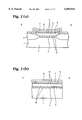
- FIG. 7 is a plan view of a memory cell portion, in which the dotted line represents an interface between an active region and a device isolation region; CG represents a control gate electrode region; and FG represents a floating gate electrode region.
- FIGS. 8(a) to 12(b) show a prior art process for manufacturing a memory cell portion.
- (a) represents an X-X' cross section of FIG. 7
- (b) represents a Y'-Y cross section of FIG. 7.
- a device isolation region 22 comprising a silicon oxide film of 500 nm and an active region 23 are formed on a P-type semiconductor substrate 21 by LOCOS method. Thereafter, a tunnel oxide film 24 is formed to a thickness of about 10 nm on the active region 23 by thermal oxidation, and then a polysilicon film 25 doped with phosphorus as an impurity is deposited to a thickness of about 100 nm as a material for a floating gate electrode.
- the polysilicon film 25 is patterned by reactive ion etching using, as a mask, a resist R11 patterned by means of photolithography so as to form the floating gate electrode, as shown in FIGS. 8(a) and 8(b).
- an ONO film (a three-layer film of first silicon oxide film 26 (SiO 2 )/silicon nitride film 27 (SiN)/second silicon oxide film 28 (SiO 2 )) is formed as an interlayer capacitive film between the floating gate electrode and the control gate electrode, as shown in FIGS. 9(a) and 9(b).
- a first silicon oxide film 26 is formed to a thickness of 8 nm on a surface of the floating gate electrode by thermal oxidation method; then a silicon nitride film 27 is formed to a thickness of 20 nm by CVD (Chemical Vapor Deposition) method; and further a second silicon oxide film 28 is formed to a thickness of 8 nm, successively.
- a polycide film 29 is deposited to a thickness of about 100 nm as a material for the control gate electrode.
- the polycide film 29 is patterned by reactive ion etching using, as a mask, a resist R22 patterned by means of photolithography so as to form the control gate electrode, as shown in FIGS. 10(a) and 10(b). Namely, the polycide film 29 as a material for the control gate electrode, the ONO film, and the polysilicon film 25 as a material for the floating gate electrode are successively removed by etching.
- a side wall of the polysilicon film 25 as a material for the floating gate electrode is covered with a thermal oxide film 30 as shown in FIGS. 11(a) and 11(b), since the side wall of the polysilicon film 25 is exposed during the patterning of the polycide film 29 for the control gate electrode.
- an impurity is implanted with the control gate electrode used as a mask to form source/drain regions 31, and an interlayer dielectric film 32 is deposited.
- the side wall of the polysilicon film as a material for the floating gate must be covered with a thermal oxide film, since the side wall of the polycrystalline film is exposed during the patterning of the polycide film 29 for the control gate electrode.
- the interlayer capacitive film is formed of an ONO film
- oxidation to the floating gate electrode and the control gate electrode proceeds from the interface between the first silicon oxide film 26 and the floating gate electrode, and from the interface between the second silicon oxide film 28 and the control gate electrode, respectively. This causes portions 26a and 28a of the ONO film adjacent the exposed side surface of the polysilicon film to be thickened, as shown in FIGS. 11(a) and 11(b).
- This partial thickening of the ONO film reduces the ratio (coupling ratio) of the potential difference between the floating gate electrode and the substrate relative to the potential difference between the control gate electrode and the substrate, thereby decreasing the efficiency of performing writing and erasing operations to the floating gate electrode by use of electrons.
- the oxidation proceeds also to the floating gate electrode from the interface between the tunnel dielectric film and the floating gate electrode as well as to the interfaces of the interlayer capacitive film, thereby thickening a portion 24a of the tunnel oxide film adjacent the exposed side surface of the polysilicon film 25.
- the electric field strength between the floating gate electrode and the diffusion layers (source/drain) decreases due to the partial thickening of the tunnel dielectric film, whereby the FN current decreases and the writing/erasing efficiency is lowered.
- Japanese Unexamined Patent Publication (Kokai) No. HEI 6(1994)-77493 provides that a side wall of nitride film is formed on a side surface of the gate electrodes.
- this is accompanied by a drawback that the process is complicated, and moreover it is not suited for size reduction of the memory cells because the side wall of nitride film protrudes over the source/drain regions.
- the side surface of the gate electrodes must be covered with a highly dielectric thermal oxide film before the side wall of nitride film is formed, it is not possible to prevent creation of a bird's beak in forming the thermal oxide film.
- Japanese Unexamined Patent Publication (Kokai) HEI 5(1993)-267684 proposes an NONO film.
- this is accompanied by a drawback that, since the control gate electrode is in contact with the oxide film, oxidation proceeds to the control gate electrode, creating a bird's beak.
- the present invention provides a process for manufacturing a non-volatile semiconductor memory device by forming a tunnel dielectric film, a floating gate electrode, an interlayer capacitive film and a control gate electrode successively on a semiconductor substrate, wherein the process comprises introducing nitrogen atoms into at least one of an interface between the semiconductor substrate and the tunnel dielectric film, an interface between the tunnel dielectric film and the floating gate electrode, an interface between the floating gate electrode and the interlayer capacitive film and an interface between the interlayer capacitive film and the control gate electrode.
- the purpose of the present invention is to provide means for preventing the thickening of interlayer capacitive film adjacent an exposed side surface of polysilicon film and the thickening of tunnel oxide film.
- FIGS. 1(a) and 1(b) are views showing a cross section of an essential part of a process for manufacturing a non-volatile semiconductor memory device according to a first embodiment of the present invention
- FIGS. 2(a) and 2(b) are views showing the cross section of the essential part of the process for manufacturing the non-volatile semiconductor memory device according to the first embodiment of the present invention
- FIGS. 3(a) and 3(b) are views showing the cross section of the essential part of the process for manufacturing the non-volatile semiconductor memory device according to the first embodiment of the present invention
- FIGS. 4(a) and 4(b) are views showing the cross section of the essential part of the process for manufacturing the non-volatile semiconductor memory device according to the first embodiment of the present invention.
- FIGS. 5(a) and 5(b) are views showing the cross section of the essential part of the process for manufacturing the non-volatile semiconductor memory device according to the first embodiment of the present invention.
- FIGS. 6(a) and 6(b) are views showing the cross section of the essential part of the process for manufacturing the non-volatile semiconductor memory device according to the first embodiment of the present invention.
- FIG. 7 is a plan view of a memory cell portion of a non-volatile semiconductor memory device
- FIGS. 8(a) and 8(b) are views showing a cross section of an essential part of a prior art process for manufacturing a non-volatile semiconductor memory device
- FIGS. 9(a) and 9(b) are views showing the cross section of the essential part of the prior art process for manufacturing the non-volatile semiconductor memory device
- FIGS. 10(a) and 10(b) are views showing the cross section of the essential part of the prior art process for manufacturing the non-volatile semiconductor memory device
- FIGS. 11(a) and 11(b) are views showing the cross section of the essential part of the prior art process for manufacturing the non-volatile semiconductor memory device.
- FIGS. 12(a) and 12(b) are views showing the cross section of the essential part of the prior art process for manufacturing the non-volatile semiconductor memory device.
- the present invention mainly relates to a process for manufacturing a non-volatile semiconductor memory device comprising a tunnel dielectric film, a floating gate electrode, an interlayer capacitive film and a control gate electrode formed in this order on a semiconductor substrate, wherein the process includes introducing nitrogen atoms into an interface between the semiconductor substrate and the tunnel dielectric film, into an interface between the tunnel dielectric film and the floating gate electrode, into an interface between the floating gate electrode and an interlayer capacitive film or into an interface between the interlayer capacitive film and the control gate electrode, or into two or more of the above interfaces.
- the semiconductor substrate to be used in the present invention may be formed of silicon, germanium, a compound semiconductor such as GaAs or InGaAs, or the like semiconductor, among which silicon substrate is preferably used.
- a device isolation film such as a LOCOS film may be formed to a thickness of about 300 to about 2000 nm on the silicon substrate.
- the material for the tunnel dielectric film is not specifically limited as long as it is a dielectric film.
- the tunnel dielectric film is preferably formed of silicon oxide film or the like, where the thickness of the film may be for example about 5 to about 30 nm.
- the tunnel dielectric film may be formed by a known method, for example, by CVD method or a thermal oxidation method in which the surface of the semiconductor substrate is thermally treated under an oxygen atmosphere at a temperature of about 700 to about 1200° C.
- the introduction of nitrogen atoms may be achieved for example by forming the tunnel dielectric film on the semiconductor substrate to a desired thickness using the above method and then carrying out a thermal treatment under an atmosphere containing nitrogen atoms at a temperature in the range of about 700 to about 1200° C.
- the atmosphere containing nitrogen atoms referred to herein may be for example a nitrogen atmosphere containing N 2 gas or an ammonia nitrogen atmosphere containing ammonia gas.
- the thermal treatment is preferably carried out in accordance with the thickness of the tunnel dielectric film.
- the CVD method or the thermal oxidation method may be carried out under an oxidizing atmosphere containing nitrogen, for example, under an N 2 O gas atmosphere.
- ion implantation may be carried out with the implantation energy being adjusted in accordance with the thickness of the obtained tunnel dielectric film.
- nitrogen atoms are introduced finally into the interface between the semiconductor substrate and the tunnel dielectric film (and/or the interface between the tunnel dielectric film and the later-mentioned floating gate electrode).
- the material for the floating gate electrode is not specifically limited as long as it can be formed into an electrode.
- the floating gate electrode is preferably formed of polysilicon film doped with an N-type impurity such as phosphorus or arsenic, or a P-type impurity such as boron at a concentration of about 1.0 ⁇ 10 19 to about 1.0 ⁇ 10 20 cm -3 , a silicide or a polycide of such polysilicon film with a high melting point metal such as W, Ta, Ti, or the like material.
- the thickness of the floating gate electrode is preferably about 80 to 350 nm.
- the material for the floating gate electrode is polysilicon, it may be formed by a known method such as CVD method using a silane gas or the like; and if the material is a metal film, it may be formed by a known method such as an EB method, a sputtering method, a vacuum vapor deposition method or the like.
- the nitrogen atoms may be introduced, for example, by impurity diffusion or ion implantation into the floating gate electrode material after the floating gate electrode material is deposited to a desired thickness by the above method.
- the dosage is preferably about 1.0 ⁇ 10 19 to about 1.0 ⁇ 10 20 cm -3 with the implantation energy being suitably adjusted in accordance with the thickness of the floating gate electrode.
- a thermal treatment is carried out.
- the thermal treatment at this time may be carried out by a known method such as RTA (Rapid Thermal Annealing), a N 2 O nitrided dielectrics grown method, or the like under an ordinary atmosphere at a temperature of about 700 to about 1200° C.
- RTA Rapid Thermal Annealing
- N 2 O nitrided dielectrics grown method or the like under an ordinary atmosphere at a temperature of about 700 to about 1200° C.
- another thermal treatment is to be carried out at a later step, it is possible to utilize it for carrying out the above-mentioned thermal treatment.
- nitrogen atoms are introduced finally into the interface between the tunnel dielectric film and the floating gate electrode and/or the interface between the floating gate electrode and the later-mentioned interlayer capacitive film.
- the electrode material into which nitrogen atoms are introduced may be patterned into a desired shape by a known method such as photolithography and etching. Alternatively, the patterning may be carried out before the introduction of nitrogen atoms into the electrode material.
- the material for the interlayer capacitive film is not specifically limited as long as it is a material having a dielectric constant of more than a predetermined value.
- the interlayer capacitive film may be formed of a monolayer of a dielectric film such as SiO 2 , SiN, ONO (SiO 2 /SiN/SiO 2 ) film, or ONON film, a ferroelectric film such as PZT or PLZT, or a laminated layer film thereof. Among these, an ONO film is preferable.
- the thickness of the interlayer capacitive film is preferably about 30 to about 100 nm and, in the case of ONO film, it is preferably about 5 to about 30 nm/about 10 to about 50 nm/about 5 to about 30 nm.
- the interlayer capacitive film may be formed by a known method such as a CVD method, a thermal oxidation method, an MOCVD method, a sol-gel method, or the like.
- the introduction may be achieved by forming an interlayer capacitive film having nitrogen atoms as mentioned above on the floating gate electrode.
- the interlayer capacitive film is an ONO film
- nitrogen atoms are introduced into the interlayer capacitive film by first forming an oxide film by a process similar to the above-mentioned method for introducing nitrogen into the tunnel dielectric film, then forming a nitride film thereon by a known method, and further forming an oxide film thereon by a process similar to the above-mentioned method for introducing nitrogen into the tunnel dielectric film.
- nitrogen may be introduced into only one of the lower oxide film and the upper oxide film.
- the interlayer capacitive film is a monolayer film formed of a material liable to be oxidized during the process or a laminated layer film including a material film liable to be oxidized, it is preferable to introduce nitrogen atoms into the material which is liable to be oxidized.
- nitrogen atoms are introduced finally into the interface between the floating gate electrode and the interlayer capacitive film (and/or the interface between the interlayer capacitive film and the later-mentioned control gate electrode).
- the control gate electrode may be formed of a material similar to the one for the floating gate electrode in a similar manner.
- nitrogen atoms are to be introduced into the interface between the interlayer capacitive film and the control gate electrode, it may be achieved by introduction of nitrogen atoms by a method similar to the one for the floating gate electrode. Through these steps, nitrogen atoms are introduced finally into the interface between the interlayer capacitive film and the control gate electrode.
- the thermal treatment may be achieved similar to the above-mentioned method.
- plan view of a memory cell portion according to the present invention is the same as the one shown in FIG. 7.
- FIGS. 1(a) to 6(b) are views showing a cross section of an essential part of a process for manufacturing a non-volatile semiconductor memory device according to an embodiment of the present invention.
- a device isolation region 2 and an active region 3 are formed of silicon oxide film to a thickness of 500 nm on a P-type semiconductor substrate 1 by LOCOS method. Then, after a thermal oxide film is formed to a desired thickness in an oxygen atmosphere at a temperature of about 800 to about 900° C., a tunnel oxide film 4 is formed to a thickness of about 10 nm while allowing the surface of the semiconductor substrate 1 on the active region 3 to contain nitrogen by carrying out a thermal treatment under N 2 atmosphere at a temperature of about 800 to about 900° C. Thereafter, a polysilicon film 5 doped with phosphorus as an impurity is deposited to a thickness of about 100 nm as a material for a floating gate electrode.
- nitrogen is implanted into the polysilicon film 5 at an implantation energy of 20 keV and in a dosage of about 4 ⁇ 10 15 cm -2 .
- the material for the floating gate electrode is etched by reactive ion etching by using, as a mask, a resist R1 patterned by means of photolithography, as shown in FIGS. 1(a) and 1(b).
- an ONO film (a three-layer film of first silicon oxide film 6 (SiO 2 )/silicon nitride film 7 (SiN)/second silicon oxide film 8 (SiO 2 )) is formed as an interlayer capacitive film between the floating gate electrode and the control gate electrode, as shown in FIGS. 2(a) and 2(b).
- the first silicon oxide film 6 is deposited to a thickness of about 8 nm on a surface of the floating gate electrode by thermal oxidation while allowing nitrogen atoms to be contained in the interface between the tunnel oxide film 4 and the floating gate electrode and the interface between the floating gate electrode and the first silicon oxide film 6.
- a silicon nitride film 7 is formed to a thickness of about 20 nm by CVD method and, further, the second silicon oxide film 8 is successively formed to a thickness of about 8 nm.
- a polycide film 9 is deposited to a thickness of about 100 nm as a material for the control gate electrode.
- nitrogen is ion-implanted into the polycide film 9 at an implantation energy of about 20 keV and in a dosage of about 4 ⁇ 10 15 cm -2 , as shown in FIGS. 3(a) and 3(b), followed by a thermal treatment under a nitrogen atmosphere at a temperature of about 800 to about 900° C. for about 30 minutes to allow the interface between the polycide film 9 and the second silicon oxide film 8 of the ONO film to contain nitrogen.
- control gate electrode and the floating gate electrode are formed by reactive ion etching by using, as a mask, a resist R2 patterned by means of photolithography, as shown in FIGS. 4(a) and 4(b).
- the polycide film 9 as a material for the control gate electrode, the ONO film, and the polysilicon film 5 as a material for the floating gate electrode are successively removed by etching.
- the side surface of the polysilicon film 5 as a material for the floating gate electrode is covered with a thermal oxide film 10, as shown in FIGS. 5(a) and 5(b), because the side surface of the polysilicon film 5 is exposed during the patterning of the polycide film 9 for the control gate electrode.
- an interlayer dielectric film 12 is deposited.
- N 2 O lower layer of the interlayer capacitive film is formed by N 2 O oxidation method.
- a device isolation region 2 and an active region 3 are formed of silicon oxide film to a thickness of 500 nm on a P-type semiconductor substrate 1 by LOCOS method in the same manner as in the first embodiment. Then, a tunnel oxide film 4 is formed to a thickness of about 10 nm while allowing nitrogen atoms to be contained in the surface of the semiconductor substrate 1 on the active region 3 by carrying out oxidation under N 2 O atmosphere.
- a polysilicon film 5 doped with phosphorus as an impurity is deposited to a thickness of about 100 nm as a material for a floating gate electrode.
- nitrogen is implanted into the polysilicon film 5 at an implantation energy of about 20 keV and in a dosage of about 4 ⁇ 10 15 cm -2 .
- the material for the floating gate electrode is etched by reactive ion etching by using, as a mask, a resist R1 patterned by means of photolithography, as shown in FIGS. 1(a) and l(b).
- a first silicon oxide film 6 is formed to a thickness of about 8 nm on a surface of the floating gate electrode while allowing nitrogen atoms to be contained in the interface between the floating gate electrode and the first silicon oxide film 6 as a lower layer of the interlayer capacitive film by carrying out thermal oxidation using a known N 2 O oxidation method, or by carrying out thermal oxidation under an oxygen atmosphere at a temperature of about 800 to about 900° C. and then carrying out an annealing treatment under a nitrogen atmosphere at a temperature of about 800 to about 900° C.
- a silicon nitride film 7 is successively deposited to a thickness of about 20 nm by CVD method and, further, a second silicon oxide film 8 is deposited to a thickness of about 8 nm.
- the subsequent steps are carried out in the same manner as in the first embodiment up to the formation of the interlayer dielectric film 12.
- the present invention prevents oxidation at the interface between the semiconductor substrate and the tunnel oxide film, the interface between the tunnel oxide film and the floating gate electrode, the interface between the floating gate electrode and the interlayer capacitive film and/or the interface between the interlayer capacitive film and the control gate electrode, as compared with prior art manufacturing methods.
- partial thickening of the interlayer capacitive film is avoided and the coupling ratio increases, so that the writing and erasing operations to the floating gate electrode by use of electrons are performed with high efficiency.
- the interface between the tunnel dielectric film and the substrate and the interface between the tunnel dielectric film and the floating gate electrode to contain nitrogen, it is possible to prevent thickening of the tunnel dielectric film at a portion where the floating gate electrode overlaps with the diffusion layers (source/drain regions), thereby inhibiting the decrease in writing and erasing efficiency.
- the present invention provides smaller influence of the thermal treatment on the thickness of the tunnel dielectric film or the interlayer capacitive film, thereby restricting the variation in the effective thickness of the tunnel dielectric film and the interlayer capacitive film, so that the present invention provides smaller variation in writing and erasing than prior art methods.
- the effect of the present invention will increase, since the increase in the effective thickness will be more noticeable in the case of the prior art tunnel dielectric film and ONO film due to partial thickening.
Landscapes
- Engineering & Computer Science (AREA)
- Microelectronics & Electronic Packaging (AREA)
- Power Engineering (AREA)
- Condensed Matter Physics & Semiconductors (AREA)
- General Physics & Mathematics (AREA)
- Physics & Mathematics (AREA)
- Computer Hardware Design (AREA)
- Ceramic Engineering (AREA)
- Manufacturing & Machinery (AREA)
- Chemical & Material Sciences (AREA)
- Chemical Kinetics & Catalysis (AREA)
- Crystallography & Structural Chemistry (AREA)
- General Chemical & Material Sciences (AREA)
- Non-Volatile Memory (AREA)
- Semiconductor Memories (AREA)
Abstract
A process for manufacturing a non-volatile semiconductor memory device by forming a tunnel dielectric film, a floating gate electrode, an interlayer capacitive film and a control gate electrode successively on a semiconductor substrate includes introducing nitrogen atoms into at least one of an interface between the floating gate electrode and the interlayer capacitive film and an interface between the interlayer capacitive film and the control gate electrode.
Description
This application is related to Japanese Patent Application No. HEI 8(1996)-315769, filed on Nov. 27, 1996 whose priority is claimed under 35 USC §119, the disclosure of which is incorporated herein by reference in its entirety.
1. Field of the Invention
The present invention relates to a process for manufacturing a non-volatile semiconductor memory device. More particularly, the present invention relates to a process for manufacturing a non-volatile semiconductor memory device comprising memory cells having a tunnel dielectric film, a floating gate electrode, a control gate electrode and an interlayer capacitive film formed between the floating gate electrode and the control gate electrode.
2. Description of the Related Arts
With reference to FIG. 7 to FIG. 12(b), an explanation is given on a general process for manufacturing a non-volatile semiconductor memory device in which memory cells having a floating gate electrode and a control gate electrode are formed on a semiconductor substrate.
FIG. 7 is a plan view of a memory cell portion, in which the dotted line represents an interface between an active region and a device isolation region; CG represents a control gate electrode region; and FG represents a floating gate electrode region. FIGS. 8(a) to 12(b) show a prior art process for manufacturing a memory cell portion. In FIG. 8(a) to FIGS. 12(b), (a) represents an X-X' cross section of FIG. 7, and (b) represents a Y'-Y cross section of FIG. 7.
First, a device isolation region 22 comprising a silicon oxide film of 500 nm and an active region 23 are formed on a P-type semiconductor substrate 21 by LOCOS method. Thereafter, a tunnel oxide film 24 is formed to a thickness of about 10 nm on the active region 23 by thermal oxidation, and then a polysilicon film 25 doped with phosphorus as an impurity is deposited to a thickness of about 100 nm as a material for a floating gate electrode.
Subsequently, the polysilicon film 25 is patterned by reactive ion etching using, as a mask, a resist R11 patterned by means of photolithography so as to form the floating gate electrode, as shown in FIGS. 8(a) and 8(b).
After the resist R11 is removed, an ONO film (a three-layer film of first silicon oxide film 26 (SiO2)/silicon nitride film 27 (SiN)/second silicon oxide film 28 (SiO2)) is formed as an interlayer capacitive film between the floating gate electrode and the control gate electrode, as shown in FIGS. 9(a) and 9(b). Namely, a first silicon oxide film 26 is formed to a thickness of 8 nm on a surface of the floating gate electrode by thermal oxidation method; then a silicon nitride film 27 is formed to a thickness of 20 nm by CVD (Chemical Vapor Deposition) method; and further a second silicon oxide film 28 is formed to a thickness of 8 nm, successively. After the ONO film is formed, a polycide film 29 is deposited to a thickness of about 100 nm as a material for the control gate electrode.
Then, the polycide film 29 is patterned by reactive ion etching using, as a mask, a resist R22 patterned by means of photolithography so as to form the control gate electrode, as shown in FIGS. 10(a) and 10(b). Namely, the polycide film 29 as a material for the control gate electrode, the ONO film, and the polysilicon film 25 as a material for the floating gate electrode are successively removed by etching.
Further, after the resist R22 is removed, a side wall of the polysilicon film 25 as a material for the floating gate electrode is covered with a thermal oxide film 30 as shown in FIGS. 11(a) and 11(b), since the side wall of the polysilicon film 25 is exposed during the patterning of the polycide film 29 for the control gate electrode. Thereafter, as shown in FIGS. 12(a) and 12(b), an impurity is implanted with the control gate electrode used as a mask to form source/drain regions 31, and an interlayer dielectric film 32 is deposited.
According to the above prior art process, the side wall of the polysilicon film as a material for the floating gate must be covered with a thermal oxide film, since the side wall of the polycrystalline film is exposed during the patterning of the polycide film 29 for the control gate electrode. At this time, in the case where the interlayer capacitive film is formed of an ONO film, oxidation to the floating gate electrode and the control gate electrode proceeds from the interface between the first silicon oxide film 26 and the floating gate electrode, and from the interface between the second silicon oxide film 28 and the control gate electrode, respectively. This causes portions 26a and 28a of the ONO film adjacent the exposed side surface of the polysilicon film to be thickened, as shown in FIGS. 11(a) and 11(b).
This partial thickening of the ONO film reduces the ratio (coupling ratio) of the potential difference between the floating gate electrode and the substrate relative to the potential difference between the control gate electrode and the substrate, thereby decreasing the efficiency of performing writing and erasing operations to the floating gate electrode by use of electrons.
Further, as shown in FIGS. 11(a) and 11(b), the oxidation proceeds also to the floating gate electrode from the interface between the tunnel dielectric film and the floating gate electrode as well as to the interfaces of the interlayer capacitive film, thereby thickening a portion 24a of the tunnel oxide film adjacent the exposed side surface of the polysilicon film 25.
Therefore, in performing writing/erasing operations by means of an FN current, the electric field strength between the floating gate electrode and the diffusion layers (source/drain) decreases due to the partial thickening of the tunnel dielectric film, whereby the FN current decreases and the writing/erasing efficiency is lowered.
In order to solve this problem, Japanese Unexamined Patent Publication (Kokai) No. HEI 6(1994)-77493 provides that a side wall of nitride film is formed on a side surface of the gate electrodes. However, this is accompanied by a drawback that the process is complicated, and moreover it is not suited for size reduction of the memory cells because the side wall of nitride film protrudes over the source/drain regions. Also, since the side surface of the gate electrodes must be covered with a highly dielectric thermal oxide film before the side wall of nitride film is formed, it is not possible to prevent creation of a bird's beak in forming the thermal oxide film.
Further, Japanese Unexamined Patent Publication (Kokai) HEI 5(1993)-267684 proposes an NONO film. However, this is accompanied by a drawback that, since the control gate electrode is in contact with the oxide film, oxidation proceeds to the control gate electrode, creating a bird's beak.
The present invention provides a process for manufacturing a non-volatile semiconductor memory device by forming a tunnel dielectric film, a floating gate electrode, an interlayer capacitive film and a control gate electrode successively on a semiconductor substrate, wherein the process comprises introducing nitrogen atoms into at least one of an interface between the semiconductor substrate and the tunnel dielectric film, an interface between the tunnel dielectric film and the floating gate electrode, an interface between the floating gate electrode and the interlayer capacitive film and an interface between the interlayer capacitive film and the control gate electrode.
Namely, the purpose of the present invention is to provide means for preventing the thickening of interlayer capacitive film adjacent an exposed side surface of polysilicon film and the thickening of tunnel oxide film.
FIGS. 1(a) and 1(b) are views showing a cross section of an essential part of a process for manufacturing a non-volatile semiconductor memory device according to a first embodiment of the present invention;
FIGS. 2(a) and 2(b) are views showing the cross section of the essential part of the process for manufacturing the non-volatile semiconductor memory device according to the first embodiment of the present invention;
FIGS. 3(a) and 3(b) are views showing the cross section of the essential part of the process for manufacturing the non-volatile semiconductor memory device according to the first embodiment of the present invention;
FIGS. 4(a) and 4(b) are views showing the cross section of the essential part of the process for manufacturing the non-volatile semiconductor memory device according to the first embodiment of the present invention;
FIGS. 5(a) and 5(b) are views showing the cross section of the essential part of the process for manufacturing the non-volatile semiconductor memory device according to the first embodiment of the present invention;
FIGS. 6(a) and 6(b) are views showing the cross section of the essential part of the process for manufacturing the non-volatile semiconductor memory device according to the first embodiment of the present invention;
FIG. 7 is a plan view of a memory cell portion of a non-volatile semiconductor memory device;
FIGS. 8(a) and 8(b) are views showing a cross section of an essential part of a prior art process for manufacturing a non-volatile semiconductor memory device;
FIGS. 9(a) and 9(b) are views showing the cross section of the essential part of the prior art process for manufacturing the non-volatile semiconductor memory device;
FIGS. 10(a) and 10(b) are views showing the cross section of the essential part of the prior art process for manufacturing the non-volatile semiconductor memory device;
FIGS. 11(a) and 11(b) are views showing the cross section of the essential part of the prior art process for manufacturing the non-volatile semiconductor memory device; and
FIGS. 12(a) and 12(b) are views showing the cross section of the essential part of the prior art process for manufacturing the non-volatile semiconductor memory device.
The present invention mainly relates to a process for manufacturing a non-volatile semiconductor memory device comprising a tunnel dielectric film, a floating gate electrode, an interlayer capacitive film and a control gate electrode formed in this order on a semiconductor substrate, wherein the process includes introducing nitrogen atoms into an interface between the semiconductor substrate and the tunnel dielectric film, into an interface between the tunnel dielectric film and the floating gate electrode, into an interface between the floating gate electrode and an interlayer capacitive film or into an interface between the interlayer capacitive film and the control gate electrode, or into two or more of the above interfaces.
The semiconductor substrate to be used in the present invention may be formed of silicon, germanium, a compound semiconductor such as GaAs or InGaAs, or the like semiconductor, among which silicon substrate is preferably used. A device isolation film such as a LOCOS film may be formed to a thickness of about 300 to about 2000 nm on the silicon substrate.
The material for the tunnel dielectric film is not specifically limited as long as it is a dielectric film. However, the tunnel dielectric film is preferably formed of silicon oxide film or the like, where the thickness of the film may be for example about 5 to about 30 nm.
The tunnel dielectric film may be formed by a known method, for example, by CVD method or a thermal oxidation method in which the surface of the semiconductor substrate is thermally treated under an oxygen atmosphere at a temperature of about 700 to about 1200° C.
In the case where nitrogen atoms are to be introduced into the interface between the semiconductor substrate and the tunnel dielectric film (and/or the interface between the tunnel dielectric film and the later-mentioned floating gate electrode), the introduction of nitrogen atoms may be achieved for example by forming the tunnel dielectric film on the semiconductor substrate to a desired thickness using the above method and then carrying out a thermal treatment under an atmosphere containing nitrogen atoms at a temperature in the range of about 700 to about 1200° C. The atmosphere containing nitrogen atoms referred to herein may be for example a nitrogen atmosphere containing N2 gas or an ammonia nitrogen atmosphere containing ammonia gas. The thermal treatment is preferably carried out in accordance with the thickness of the tunnel dielectric film.
Alternatively, the CVD method or the thermal oxidation method may be carried out under an oxidizing atmosphere containing nitrogen, for example, under an N2 O gas atmosphere.
Still alternatively, after a tunnel dielectric film is formed on the semiconductor substrate to a desired thickness by the above method, ion implantation may be carried out with the implantation energy being adjusted in accordance with the thickness of the obtained tunnel dielectric film.
Through one of these methods, nitrogen atoms are introduced finally into the interface between the semiconductor substrate and the tunnel dielectric film (and/or the interface between the tunnel dielectric film and the later-mentioned floating gate electrode).
The material for the floating gate electrode is not specifically limited as long as it can be formed into an electrode. For example, the floating gate electrode is preferably formed of polysilicon film doped with an N-type impurity such as phosphorus or arsenic, or a P-type impurity such as boron at a concentration of about 1.0×10¹⁹ to about 1.0×1020 cm-3, a silicide or a polycide of such polysilicon film with a high melting point metal such as W, Ta, Ti, or the like material. The thickness of the floating gate electrode is preferably about 80 to 350 nm.
If the material for the floating gate electrode is polysilicon, it may be formed by a known method such as CVD method using a silane gas or the like; and if the material is a metal film, it may be formed by a known method such as an EB method, a sputtering method, a vacuum vapor deposition method or the like.
In the case where nitrogen atoms are to be introduced into the interface between the tunnel dielectric film and the floating gate electrode, and/or the interface between the floating gate electrode and the later-mentioned interlayer capacitive film, the nitrogen atoms may be introduced, for example, by impurity diffusion or ion implantation into the floating gate electrode material after the floating gate electrode material is deposited to a desired thickness by the above method. Specifically, in the case of ion implantation, the dosage is preferably about 1.0×10¹⁹ to about 1.0×1020 cm-3 with the implantation energy being suitably adjusted in accordance with the thickness of the floating gate electrode.
After the introduction of nitrogen atoms, a thermal treatment is carried out. The thermal treatment at this time may be carried out by a known method such as RTA (Rapid Thermal Annealing), a N2 O nitrided dielectrics grown method, or the like under an ordinary atmosphere at a temperature of about 700 to about 1200° C. Here, if another thermal treatment is to be carried out at a later step, it is possible to utilize it for carrying out the above-mentioned thermal treatment.
Through these steps, nitrogen atoms are introduced finally into the interface between the tunnel dielectric film and the floating gate electrode and/or the interface between the floating gate electrode and the later-mentioned interlayer capacitive film.
The electrode material into which nitrogen atoms are introduced may be patterned into a desired shape by a known method such as photolithography and etching. Alternatively, the patterning may be carried out before the introduction of nitrogen atoms into the electrode material.
The material for the interlayer capacitive film is not specifically limited as long as it is a material having a dielectric constant of more than a predetermined value. The interlayer capacitive film may be formed of a monolayer of a dielectric film such as SiO2, SiN, ONO (SiO2 /SiN/SiO2) film, or ONON film, a ferroelectric film such as PZT or PLZT, or a laminated layer film thereof. Among these, an ONO film is preferable. The thickness of the interlayer capacitive film is preferably about 30 to about 100 nm and, in the case of ONO film, it is preferably about 5 to about 30 nm/about 10 to about 50 nm/about 5 to about 30 nm.
The interlayer capacitive film may be formed by a known method such as a CVD method, a thermal oxidation method, an MOCVD method, a sol-gel method, or the like.
In the case where nitrogen atoms are to be introduced into the interface between the floating gate electrode and the interlayer capacitive film (and/or the interface between the interlayer capacitive film and the later-mentioned control gate electrode), the introduction may be achieved by forming an interlayer capacitive film having nitrogen atoms as mentioned above on the floating gate electrode. Specifically, in the case where the interlayer capacitive film is an ONO film, nitrogen atoms are introduced into the interlayer capacitive film by first forming an oxide film by a process similar to the above-mentioned method for introducing nitrogen into the tunnel dielectric film, then forming a nitride film thereon by a known method, and further forming an oxide film thereon by a process similar to the above-mentioned method for introducing nitrogen into the tunnel dielectric film. In this case, nitrogen may be introduced into only one of the lower oxide film and the upper oxide film.
If the interlayer capacitive film is a monolayer film formed of a material liable to be oxidized during the process or a laminated layer film including a material film liable to be oxidized, it is preferable to introduce nitrogen atoms into the material which is liable to be oxidized.
Through these steps, nitrogen atoms are introduced finally into the interface between the floating gate electrode and the interlayer capacitive film (and/or the interface between the interlayer capacitive film and the later-mentioned control gate electrode).
The control gate electrode may be formed of a material similar to the one for the floating gate electrode in a similar manner. In the case where nitrogen atoms are to be introduced into the interface between the interlayer capacitive film and the control gate electrode, it may be achieved by introduction of nitrogen atoms by a method similar to the one for the floating gate electrode. Through these steps, nitrogen atoms are introduced finally into the interface between the interlayer capacitive film and the control gate electrode.
After the introduction of nitrogen atoms, a thermal treatment is carried out. The thermal treatment may be achieved similar to the above-mentioned method.
The present invention is now explained in detail by way of embodiments with reference to the attached drawings.
The plan view of a memory cell portion according to the present invention is the same as the one shown in FIG. 7.
FIGS. 1(a) to 6(b) are views showing a cross section of an essential part of a process for manufacturing a non-volatile semiconductor memory device according to an embodiment of the present invention.
With reference to FIGS. 1(a) to 6(b), a process for manufacturing a non-volatile semiconductor memory device according to the first embodiment of the present invention is hereafter described in detail.
First, a device isolation region 2 and an active region 3 are formed of silicon oxide film to a thickness of 500 nm on a P-type semiconductor substrate 1 by LOCOS method. Then, after a thermal oxide film is formed to a desired thickness in an oxygen atmosphere at a temperature of about 800 to about 900° C., a tunnel oxide film 4 is formed to a thickness of about 10 nm while allowing the surface of the semiconductor substrate 1 on the active region 3 to contain nitrogen by carrying out a thermal treatment under N2 atmosphere at a temperature of about 800 to about 900° C. Thereafter, a polysilicon film 5 doped with phosphorus as an impurity is deposited to a thickness of about 100 nm as a material for a floating gate electrode.
Then, nitrogen is implanted into the polysilicon film 5 at an implantation energy of 20 keV and in a dosage of about 4×1015 cm-2. Further, the material for the floating gate electrode is etched by reactive ion etching by using, as a mask, a resist R1 patterned by means of photolithography, as shown in FIGS. 1(a) and 1(b).
After the resist R1 is removed, an ONO film (a three-layer film of first silicon oxide film 6 (SiO2)/silicon nitride film 7 (SiN)/second silicon oxide film 8 (SiO2)) is formed as an interlayer capacitive film between the floating gate electrode and the control gate electrode, as shown in FIGS. 2(a) and 2(b).
Namely, the first silicon oxide film 6 is deposited to a thickness of about 8 nm on a surface of the floating gate electrode by thermal oxidation while allowing nitrogen atoms to be contained in the interface between the tunnel oxide film 4 and the floating gate electrode and the interface between the floating gate electrode and the first silicon oxide film 6. Then, a silicon nitride film 7 is formed to a thickness of about 20 nm by CVD method and, further, the second silicon oxide film 8 is successively formed to a thickness of about 8 nm. After the ONO film is formed, a polycide film 9 is deposited to a thickness of about 100 nm as a material for the control gate electrode.
Subsequently, nitrogen is ion-implanted into the polycide film 9 at an implantation energy of about 20 keV and in a dosage of about 4×1015 cm-2, as shown in FIGS. 3(a) and 3(b), followed by a thermal treatment under a nitrogen atmosphere at a temperature of about 800 to about 900° C. for about 30 minutes to allow the interface between the polycide film 9 and the second silicon oxide film 8 of the ONO film to contain nitrogen.
Thereafter, the control gate electrode and the floating gate electrode are formed by reactive ion etching by using, as a mask, a resist R2 patterned by means of photolithography, as shown in FIGS. 4(a) and 4(b). Namely, the polycide film 9 as a material for the control gate electrode, the ONO film, and the polysilicon film 5 as a material for the floating gate electrode are successively removed by etching.
Then, after the resist R2 is removed, the side surface of the polysilicon film 5 as a material for the floating gate electrode is covered with a thermal oxide film 10, as shown in FIGS. 5(a) and 5(b), because the side surface of the polysilicon film 5 is exposed during the patterning of the polycide film 9 for the control gate electrode.
Subsequently, after an impurity is implanted with the control gate electrode used as a mask to form source/drain regions 11, an interlayer dielectric film 12 is deposited.
Next, an explanation is hereafter given on a process for manufacturing a non-volatile semiconductor memory device according to the second embodiment of the present invention, in which N2 O lower layer of the interlayer capacitive film is formed by N2 O oxidation method.
First, a device isolation region 2 and an active region 3 are formed of silicon oxide film to a thickness of 500 nm on a P-type semiconductor substrate 1 by LOCOS method in the same manner as in the first embodiment. Then, a tunnel oxide film 4 is formed to a thickness of about 10 nm while allowing nitrogen atoms to be contained in the surface of the semiconductor substrate 1 on the active region 3 by carrying out oxidation under N2 O atmosphere.
Thereafter, a polysilicon film 5 doped with phosphorus as an impurity is deposited to a thickness of about 100 nm as a material for a floating gate electrode. Then, nitrogen is implanted into the polysilicon film 5 at an implantation energy of about 20 keV and in a dosage of about 4×1015 cm-2. Further, the material for the floating gate electrode is etched by reactive ion etching by using, as a mask, a resist R1 patterned by means of photolithography, as shown in FIGS. 1(a) and l(b).
Subsequently, an ONO film is formed, as shown in FIGS. 2(a) and 2(b). Namely, a first silicon oxide film 6 is formed to a thickness of about 8 nm on a surface of the floating gate electrode while allowing nitrogen atoms to be contained in the interface between the floating gate electrode and the first silicon oxide film 6 as a lower layer of the interlayer capacitive film by carrying out thermal oxidation using a known N2 O oxidation method, or by carrying out thermal oxidation under an oxygen atmosphere at a temperature of about 800 to about 900° C. and then carrying out an annealing treatment under a nitrogen atmosphere at a temperature of about 800 to about 900° C. Thereafter, a silicon nitride film 7 is successively deposited to a thickness of about 20 nm by CVD method and, further, a second silicon oxide film 8 is deposited to a thickness of about 8 nm. The subsequent steps are carried out in the same manner as in the first embodiment up to the formation of the interlayer dielectric film 12.
As shown above, the present invention prevents oxidation at the interface between the semiconductor substrate and the tunnel oxide film, the interface between the tunnel oxide film and the floating gate electrode, the interface between the floating gate electrode and the interlayer capacitive film and/or the interface between the interlayer capacitive film and the control gate electrode, as compared with prior art manufacturing methods. As a result, partial thickening of the interlayer capacitive film is avoided and the coupling ratio increases, so that the writing and erasing operations to the floating gate electrode by use of electrons are performed with high efficiency.
Also, by allowing the interface between the tunnel dielectric film and the substrate and the interface between the tunnel dielectric film and the floating gate electrode to contain nitrogen, it is possible to prevent thickening of the tunnel dielectric film at a portion where the floating gate electrode overlaps with the diffusion layers (source/drain regions), thereby inhibiting the decrease in writing and erasing efficiency.
Further, the present invention provides smaller influence of the thermal treatment on the thickness of the tunnel dielectric film or the interlayer capacitive film, thereby restricting the variation in the effective thickness of the tunnel dielectric film and the interlayer capacitive film, so that the present invention provides smaller variation in writing and erasing than prior art methods.
Furthermore, according as the size reduction of the devices proceeds, the effect of the present invention will increase, since the increase in the effective thickness will be more noticeable in the case of the prior art tunnel dielectric film and ONO film due to partial thickening.
Although the present invention has fully been described by way of example with reference to the accompanying drawings, it is to be understood that various changes and modifications will be apparent to those skilled in the art. Therefore, unless otherwise such changes and modifications depart from the spirit and scope of the invention, they should be construed as being included therein.
Claims (4)
1. A process for manufacturing a non-volatile semiconductor memory device by forming a tunnel dielectric film, a floating gate electrode, an interlayer capacitive film and a control gate electrode successively on a semiconductor substrate, wherein the process comprises introducing nitrogen atoms into at least an interface between the floating gate electrode and the interlayer capacitive film and an interface between the interlayer capacitive film and the control gate electrode.
2. A process for manufacturing a non-volatile semiconductor memory device according to claim 1, wherein introduction of nitrogen atoms into the interface between the tunnel dielectric film and the floating gate electrode and the interface between the floating gate electrode and the interlayer capacitive film is performed by the steps of forming the floating gate electrode on the tunnel dielectric film, then doping nitrogen atoms into the floating gate electrode, depositing the interlayer capacitive film on the floating gate electrode and carrying out a thermal treatment.
3. A process for manufacturing a non-volatile semiconductor memory device according to claim 1, wherein introduction of nitrogen atoms into the interface between the interlayer capacitive film and the control gate electrode is performed by the steps of forming the control gate electrode on the interlayer capacitive film, then doping nitrogen atoms into the control gate electrode and carrying out a thermal treatment.
4. A process for manufacturing a non-volatile semiconductor memory device according to claim 3, wherein introduction of nitrogen atoms into the interface between the tunnel dielectric film and the floating gate electrode and into the interface between the floating gate electrode and the interlayer capacitive film is performed by the steps of forming the floating gate electrode on the tunnel dielectric film, then doping nitrogen atoms into the floating gate electrode, depositing the interlayer capacitive film on the floating gate electrode and carrying out a thermal treatment.
Applications Claiming Priority (2)
| Application Number | Priority Date | Filing Date | Title |
|---|---|---|---|
| JP31576996A JP3312102B2 (en) | 1996-11-27 | 1996-11-27 | Manufacturing method of nonvolatile semiconductor memory device |
| JP8-315769 | 1996-11-27 |
Publications (1)
| Publication Number | Publication Date |
|---|---|
| US6069041A true US6069041A (en) | 2000-05-30 |
Family
ID=18069332
Family Applications (1)
| Application Number | Title | Priority Date | Filing Date |
|---|---|---|---|
| US08/974,158 Expired - Lifetime US6069041A (en) | 1996-11-27 | 1997-11-19 | Process for manufacturing non-volatile semiconductor memory device by introducing nitrogen atoms |
Country Status (2)
| Country | Link |
|---|---|
| US (1) | US6069041A (en) |
| JP (1) | JP3312102B2 (en) |
Cited By (27)
| Publication number | Priority date | Publication date | Assignee | Title |
|---|---|---|---|---|
| US6184088B1 (en) * | 1996-03-29 | 2001-02-06 | Sanyo Electric Co., Ltd. | Method for manufacturing a split game type transistor |
| US6248632B1 (en) * | 1998-12-24 | 2001-06-19 | Hyundai Electronics Industries Co., Ltd. | Method of forming gate electrode with polycide structure in semiconductor device |
| US6255169B1 (en) * | 1999-02-22 | 2001-07-03 | Advanced Micro Devices, Inc. | Process for fabricating a high-endurance non-volatile memory device |
| US6294430B1 (en) * | 2000-01-31 | 2001-09-25 | Advanced Micro Devices, Inc. | Nitridization of the pre-ddi screen oxide |
| US6319775B1 (en) * | 1999-10-25 | 2001-11-20 | Advanced Micro Devices, Inc. | Nitridation process for fabricating an ONO floating-gate electrode in a two-bit EEPROM device |
| WO2001097291A1 (en) | 2000-06-14 | 2001-12-20 | Infineon Technologies Ag | Method for producing a field effect transistor having a floating gate |
| US6399519B1 (en) * | 1999-12-07 | 2002-06-04 | Advanced Micro Devices, Inc. | Method for establishing ultra-thin gate insulator having annealed oxide and oxidized nitride |
| US6399984B1 (en) * | 2000-07-03 | 2002-06-04 | Advanced Micro Devices, Inc. | Species implantation for minimizing interface defect density in flash memory devices |
| US6498374B1 (en) * | 1999-07-01 | 2002-12-24 | Kabushiki Kaisha Toshiba | MOS semiconductor device having gate insulating film containing nitrogen |
| US20020195668A1 (en) * | 2001-06-22 | 2002-12-26 | Tetsuo Endoh | Semiconductor memory and its production process |
| US6614081B2 (en) * | 2000-04-05 | 2003-09-02 | Nec Electronics Corporation | High-performance MOS transistor of LDD structure having a gate insulating film with a nitride central portion and oxide end portions |
| US6737689B1 (en) * | 1998-12-10 | 2004-05-18 | Infineon Technologies Ag | FEMFET device and method for producing same |
| US6989319B1 (en) * | 1998-08-28 | 2006-01-24 | Advanced Micro Devices, Inc. | Methods for forming nitrogen-rich regions in non-volatile semiconductor memory devices |
| US20060151824A1 (en) * | 2002-07-05 | 2006-07-13 | Chang-Hyun Lee | Flash memory devices having self aligned shallow trench isolation structures |
| US20060202259A1 (en) * | 2005-03-09 | 2006-09-14 | Yoshio Ozawa | Semiconductor device and method of fabricating the same |
| US20070196985A1 (en) * | 2005-04-26 | 2007-08-23 | Yoshio Ozawa | Semiconductor memory device and method of manufacturing the same |
| FR2899377A1 (en) * | 2006-03-30 | 2007-10-05 | Centre Nat Rech Scient | Multilayer thin film microstructure and nanostructure forming method for photonics field, involves implanting ionic elements on active layers across resist to modify properties of layers to obtain structure with controlled properties |
| US20080014729A1 (en) * | 2006-07-12 | 2008-01-17 | Samsung Electronics Co., Ltd. | Method of manufacturing a memory device |
| CN100378964C (en) * | 2005-01-13 | 2008-04-02 | 海力士半导体有限公司 | Method of manufacturing a flash memory device |
| US20080157175A1 (en) * | 2006-12-27 | 2008-07-03 | Dae Young Kim | Flash Memory Device and Method for Manufacturing Thereof |
| US20090039406A1 (en) * | 2005-04-15 | 2009-02-12 | Tokyo Electron Limited | Semiconductor device manufacturing method, semiconductor device, plasma nitriding treatment method, control program and computer storage medium |
| US20090045472A1 (en) * | 2007-08-13 | 2009-02-19 | Texas Instruments Incorporated | Methodology for Reducing Post Burn-In Vmin Drift |
| US7566929B2 (en) | 2002-07-05 | 2009-07-28 | Samsung Electronics Co., Ltd. | Nonvolatile memory devices having floating gate electrodes with nitrogen-doped layers on portions thereof |
| US20090309150A1 (en) * | 2008-06-13 | 2009-12-17 | Infineon Technologies Ag | Semiconductor Device And Method For Making Semiconductor Device |
| US20100009503A1 (en) * | 2008-07-09 | 2010-01-14 | Kai James K | Method of forming dielectric layer above floating gate for reducing leakage current |
| US20100006915A1 (en) * | 2008-07-09 | 2010-01-14 | Dana Lee | Dielectric layer above floating gate for reducing leakage current |
| US20100081267A1 (en) * | 2008-09-30 | 2010-04-01 | Vinod Robert Purayath | Method for forming self-aligned dielectric cap above floating gate |
Families Citing this family (6)
| Publication number | Priority date | Publication date | Assignee | Title |
|---|---|---|---|---|
| KR100426482B1 (en) * | 2001-12-22 | 2004-04-14 | 주식회사 하이닉스반도체 | Method of manufacturing a flash memory cell |
| KR100466312B1 (en) * | 2002-08-07 | 2005-01-13 | 삼성전자주식회사 | Method of manufacturing semiconductor device having an ONO layer |
| KR100644397B1 (en) | 2005-04-07 | 2006-11-10 | 삼성전자주식회사 | Method of Treating Thin Layer and Method of Manufacturing Non-Volatile Memory Cell Using the same |
| JP4764267B2 (en) * | 2006-06-27 | 2011-08-31 | 株式会社東芝 | Semiconductor device and manufacturing method thereof |
| JP2008211022A (en) * | 2007-02-27 | 2008-09-11 | Toshiba Corp | Nonvolatile semiconductor memory device and method of manufacturing the same |
| JP5313547B2 (en) * | 2008-05-09 | 2013-10-09 | 東京エレクトロン株式会社 | Manufacturing method of semiconductor device |
Citations (7)
| Publication number | Priority date | Publication date | Assignee | Title |
|---|---|---|---|---|
| US4774197A (en) * | 1986-06-17 | 1988-09-27 | Advanced Micro Devices, Inc. | Method of improving silicon dioxide |
| JPH05267684A (en) * | 1992-03-18 | 1993-10-15 | Rohm Co Ltd | Nonvolatile storage element |
| JPH0629314A (en) * | 1992-07-08 | 1994-02-04 | Hitachi Ltd | Semiconductor device and manufacture thereof |
| JPH0677493A (en) * | 1992-08-27 | 1994-03-18 | Mitsubishi Electric Corp | Semiconductor device and its manufacture |
| US5464792A (en) * | 1993-06-07 | 1995-11-07 | Motorola, Inc. | Process to incorporate nitrogen at an interface of a dielectric layer in a semiconductor device |
| US5571734A (en) * | 1994-10-03 | 1996-11-05 | Motorola, Inc. | Method for forming a fluorinated nitrogen containing dielectric |
| US5837585A (en) * | 1996-07-23 | 1998-11-17 | Vanguard International Semiconductor Corporation | Method of fabricating flash memory cell |
-
1996
- 1996-11-27 JP JP31576996A patent/JP3312102B2/en not_active Expired - Fee Related
-
1997
- 1997-11-19 US US08/974,158 patent/US6069041A/en not_active Expired - Lifetime
Patent Citations (7)
| Publication number | Priority date | Publication date | Assignee | Title |
|---|---|---|---|---|
| US4774197A (en) * | 1986-06-17 | 1988-09-27 | Advanced Micro Devices, Inc. | Method of improving silicon dioxide |
| JPH05267684A (en) * | 1992-03-18 | 1993-10-15 | Rohm Co Ltd | Nonvolatile storage element |
| JPH0629314A (en) * | 1992-07-08 | 1994-02-04 | Hitachi Ltd | Semiconductor device and manufacture thereof |
| JPH0677493A (en) * | 1992-08-27 | 1994-03-18 | Mitsubishi Electric Corp | Semiconductor device and its manufacture |
| US5464792A (en) * | 1993-06-07 | 1995-11-07 | Motorola, Inc. | Process to incorporate nitrogen at an interface of a dielectric layer in a semiconductor device |
| US5571734A (en) * | 1994-10-03 | 1996-11-05 | Motorola, Inc. | Method for forming a fluorinated nitrogen containing dielectric |
| US5837585A (en) * | 1996-07-23 | 1998-11-17 | Vanguard International Semiconductor Corporation | Method of fabricating flash memory cell |
Non-Patent Citations (2)
| Title |
|---|
| T. Kuroi, et al., 1994, Symposium on VLSI Technology Digest of Technical Papers, "The Effects of Nitrogen Implantation of into P Poly-Silicon Gate on Gate Oxide Properties", pp. 107-108. |
| T. Kuroi, et al., 1994, Symposium on VLSI Technology Digest of Technical Papers, The Effects of Nitrogen Implantation of into P Poly Silicon Gate on Gate Oxide Properties , pp. 107 108. * |
Cited By (49)
| Publication number | Priority date | Publication date | Assignee | Title |
|---|---|---|---|---|
| US6184088B1 (en) * | 1996-03-29 | 2001-02-06 | Sanyo Electric Co., Ltd. | Method for manufacturing a split game type transistor |
| US6989319B1 (en) * | 1998-08-28 | 2006-01-24 | Advanced Micro Devices, Inc. | Methods for forming nitrogen-rich regions in non-volatile semiconductor memory devices |
| US6737689B1 (en) * | 1998-12-10 | 2004-05-18 | Infineon Technologies Ag | FEMFET device and method for producing same |
| US6248632B1 (en) * | 1998-12-24 | 2001-06-19 | Hyundai Electronics Industries Co., Ltd. | Method of forming gate electrode with polycide structure in semiconductor device |
| US6255169B1 (en) * | 1999-02-22 | 2001-07-03 | Advanced Micro Devices, Inc. | Process for fabricating a high-endurance non-volatile memory device |
| US6498374B1 (en) * | 1999-07-01 | 2002-12-24 | Kabushiki Kaisha Toshiba | MOS semiconductor device having gate insulating film containing nitrogen |
| US6319775B1 (en) * | 1999-10-25 | 2001-11-20 | Advanced Micro Devices, Inc. | Nitridation process for fabricating an ONO floating-gate electrode in a two-bit EEPROM device |
| US6399519B1 (en) * | 1999-12-07 | 2002-06-04 | Advanced Micro Devices, Inc. | Method for establishing ultra-thin gate insulator having annealed oxide and oxidized nitride |
| US6294430B1 (en) * | 2000-01-31 | 2001-09-25 | Advanced Micro Devices, Inc. | Nitridization of the pre-ddi screen oxide |
| US20040026752A1 (en) * | 2000-04-05 | 2004-02-12 | Nec Electronics Corporation | High-performance MOS transistor of LDD structure having a gate insulating film with a nitride central portion and oxide end portions |
| US6794258B2 (en) | 2000-04-05 | 2004-09-21 | Nec Electronics Corporation | High-performance MOS transistor of LDD structure having a gate insulating film with a nitride central portion and oxide end portions |
| US6614081B2 (en) * | 2000-04-05 | 2003-09-02 | Nec Electronics Corporation | High-performance MOS transistor of LDD structure having a gate insulating film with a nitride central portion and oxide end portions |
| US20030119261A1 (en) * | 2000-06-14 | 2003-06-26 | Franz Hofmann | Method for fabricating a field-effect transistor having a floating gate |
| WO2001097291A1 (en) | 2000-06-14 | 2001-12-20 | Infineon Technologies Ag | Method for producing a field effect transistor having a floating gate |
| US7060558B2 (en) * | 2000-06-14 | 2006-06-13 | Infineon Technologies Ag | Method for fabricating a field-effect transistor having a floating gate |
| US6399984B1 (en) * | 2000-07-03 | 2002-06-04 | Advanced Micro Devices, Inc. | Species implantation for minimizing interface defect density in flash memory devices |
| US20020195668A1 (en) * | 2001-06-22 | 2002-12-26 | Tetsuo Endoh | Semiconductor memory and its production process |
| US6933556B2 (en) * | 2001-06-22 | 2005-08-23 | Fujio Masuoka | Semiconductor memory with gate at least partially located in recess defined in vertically oriented semiconductor layer |
| US20060151824A1 (en) * | 2002-07-05 | 2006-07-13 | Chang-Hyun Lee | Flash memory devices having self aligned shallow trench isolation structures |
| US8552488B2 (en) | 2002-07-05 | 2013-10-08 | Samsung Electronics Co., Ltd. | Nonvolatile memory devices having gate structures doped by nitrogen |
| US8008153B2 (en) | 2002-07-05 | 2011-08-30 | Samsung Electronics Co., Ltd. | Methods of fabricating nonvolatile memory devices having gate structures doped by nitrogen |
| US7566929B2 (en) | 2002-07-05 | 2009-07-28 | Samsung Electronics Co., Ltd. | Nonvolatile memory devices having floating gate electrodes with nitrogen-doped layers on portions thereof |
| US7445994B2 (en) | 2002-07-05 | 2008-11-04 | Samsung Electronics Co., Ltd. | Methods of forming non-volatile memory devices using selective nitridation techniques |
| CN100378964C (en) * | 2005-01-13 | 2008-04-02 | 海力士半导体有限公司 | Method of manufacturing a flash memory device |
| US20060202259A1 (en) * | 2005-03-09 | 2006-09-14 | Yoshio Ozawa | Semiconductor device and method of fabricating the same |
| US8026133B2 (en) | 2005-03-09 | 2011-09-27 | Kabushiki Kaisha Toshiba | Method of fabricating a semiconductor device with a non-uniform gate insulating film |
| US20090269894A1 (en) * | 2005-03-09 | 2009-10-29 | Kabushiki Kaisha Toshiba | Semiconductor device and method of fabricating the same cross-reference to related applications |
| CN101069274B (en) * | 2005-04-15 | 2010-05-19 | 东京毅力科创株式会社 | Semiconductor device manufacturing method, plasma nitriding treatment method |
| CN101908484B (en) * | 2005-04-15 | 2012-06-13 | 东京毅力科创株式会社 | Plasma nitridation treatment method |
| US20090039406A1 (en) * | 2005-04-15 | 2009-02-12 | Tokyo Electron Limited | Semiconductor device manufacturing method, semiconductor device, plasma nitriding treatment method, control program and computer storage medium |
| US7910493B2 (en) | 2005-04-15 | 2011-03-22 | Tokyo Electron Limited | Semiconductor device manufacturing method, semiconductor device, plasma nitriding treatment method, control program and computer storage medium |
| US7723772B2 (en) | 2005-04-26 | 2010-05-25 | Kabushiki Kaisha Toshiba | Semiconductor memory device and method of manufacturing the same |
| US7927949B2 (en) | 2005-04-26 | 2011-04-19 | Kabushiki Kaisha Toshiba | Semiconductor memory device and method of manufacturing the same |
| US20070196985A1 (en) * | 2005-04-26 | 2007-08-23 | Yoshio Ozawa | Semiconductor memory device and method of manufacturing the same |
| US20100197130A1 (en) * | 2005-04-26 | 2010-08-05 | Kabushiki Kaisha Toshiba | Semiconductor memory device and method of manufacturing the same |
| WO2007113194A1 (en) * | 2006-03-30 | 2007-10-11 | Centre National De La Recherche Scientifique (Cnrs) | Method of producing multilayer structures having controlled properties |
| US20100291315A1 (en) * | 2006-03-30 | 2010-11-18 | Centre National De La Recherche Scientifique (Cnrs | Method of Producing Multilayer Structures Having Controlled Properties |
| FR2899377A1 (en) * | 2006-03-30 | 2007-10-05 | Centre Nat Rech Scient | Multilayer thin film microstructure and nanostructure forming method for photonics field, involves implanting ionic elements on active layers across resist to modify properties of layers to obtain structure with controlled properties |
| US20080014729A1 (en) * | 2006-07-12 | 2008-01-17 | Samsung Electronics Co., Ltd. | Method of manufacturing a memory device |
| US20080157175A1 (en) * | 2006-12-27 | 2008-07-03 | Dae Young Kim | Flash Memory Device and Method for Manufacturing Thereof |
| US20090045472A1 (en) * | 2007-08-13 | 2009-02-19 | Texas Instruments Incorporated | Methodology for Reducing Post Burn-In Vmin Drift |
| US20090309150A1 (en) * | 2008-06-13 | 2009-12-17 | Infineon Technologies Ag | Semiconductor Device And Method For Making Semiconductor Device |
| DE102009011880B4 (en) | 2008-06-13 | 2019-08-14 | Infineon Technologies Ag | Memory device with a high-k dielectric layer and method for its production |
| US7919809B2 (en) | 2008-07-09 | 2011-04-05 | Sandisk Corporation | Dielectric layer above floating gate for reducing leakage current |
| US7915124B2 (en) * | 2008-07-09 | 2011-03-29 | Sandisk Corporation | Method of forming dielectric layer above floating gate for reducing leakage current |
| US20100009503A1 (en) * | 2008-07-09 | 2010-01-14 | Kai James K | Method of forming dielectric layer above floating gate for reducing leakage current |
| US20100006915A1 (en) * | 2008-07-09 | 2010-01-14 | Dana Lee | Dielectric layer above floating gate for reducing leakage current |
| US20100081267A1 (en) * | 2008-09-30 | 2010-04-01 | Vinod Robert Purayath | Method for forming self-aligned dielectric cap above floating gate |
| US8207036B2 (en) | 2008-09-30 | 2012-06-26 | Sandisk Technologies Inc. | Method for forming self-aligned dielectric cap above floating gate |
Also Published As
| Publication number | Publication date |
|---|---|
| JPH10163348A (en) | 1998-06-19 |
| JP3312102B2 (en) | 2002-08-05 |
Similar Documents
| Publication | Publication Date | Title |
|---|---|---|
| US6069041A (en) | Process for manufacturing non-volatile semiconductor memory device by introducing nitrogen atoms | |
| US6074917A (en) | LPCVD oxide and RTA for top oxide of ONO film to improve reliability for flash memory devices | |
| US5661056A (en) | Non-volatile semiconductor memory device and method of manufacturing the same | |
| US5861347A (en) | Method for forming a high voltage gate dielectric for use in integrated circuit | |
| US5836772A (en) | Interpoly dielectric process | |
| EP1247299B1 (en) | Encapsulated tungsten gate mos transistor and memory cell and method of making same | |
| US5767558A (en) | Structures for preventing gate oxide degradation | |
| US6309927B1 (en) | Method of forming high K tantalum pentoxide Ta2O5 instead of ONO stacked films to increase coupling ratio and improve reliability for flash memory devices | |
| JPH0259633B2 (en) | ||
| US6043124A (en) | Method for forming high density nonvolatile memories with high capacitive-coupling ratio | |
| US5716891A (en) | Fabrication process of semiconductor device | |
| US6143608A (en) | Barrier layer decreases nitrogen contamination of peripheral gate regions during tunnel oxide nitridation | |
| KR100466312B1 (en) | Method of manufacturing semiconductor device having an ONO layer | |
| US6399466B2 (en) | Method of manufacturing non-volatile semiconductor memory device storing charge in gate insulating layer therein | |
| US6362045B1 (en) | Method to form non-volatile memory cells | |
| JP2004179624A (en) | Method of manufacturing semiconductor device | |
| JP2001308207A (en) | Method for fabricating nonvolatile semiconductor memory device | |
| EP0195902B1 (en) | Dual electron injection structure and process with self-limiting oxidation barrier | |
| US6171927B1 (en) | Device with differential field isolation thicknesses and related methods | |
| US6380029B1 (en) | Method of forming ono stacked films and DCS tungsten silicide gate to improve polycide gate performance for flash memory devices | |
| US4735919A (en) | Method of making a floating gate memory cell | |
| US6759296B2 (en) | Method of manufacturing a flash memory cell | |
| US6162684A (en) | Ammonia annealed and wet oxidized LPCVD oxide to replace ono films for high integrated flash memory devices | |
| JP3406811B2 (en) | Semiconductor device and manufacturing method thereof | |
| US6140246A (en) | In-situ P doped amorphous silicon by NH3 to form oxidation resistant and finer grain floating gates |
Legal Events
| Date | Code | Title | Description |
|---|---|---|---|
| AS | Assignment |
Owner name: SHARP KABUSHIKI KAISHA, JAPAN Free format text: ASSIGNMENT OF ASSIGNORS INTEREST;ASSIGNORS:TANIGAMI, TAKUJI;SATO, SHINICHI;AZUMA, KENICHI;REEL/FRAME:008878/0754 Effective date: 19971114 |
|
| STCF | Information on status: patent grant |
Free format text: PATENTED CASE |
|
| FEPP | Fee payment procedure |
Free format text: PAYOR NUMBER ASSIGNED (ORIGINAL EVENT CODE: ASPN); ENTITY STATUS OF PATENT OWNER: LARGE ENTITY |
|
| FPAY | Fee payment |
Year of fee payment: 4 |
|
| FPAY | Fee payment |
Year of fee payment: 8 |
|
| FPAY | Fee payment |
Year of fee payment: 12 |