US6054883A - High accuracy 90° phase shift circuit error detection - Google Patents
High accuracy 90° phase shift circuit error detection Download PDFInfo
- Publication number
- US6054883A US6054883A US09/104,107 US10410798A US6054883A US 6054883 A US6054883 A US 6054883A US 10410798 A US10410798 A US 10410798A US 6054883 A US6054883 A US 6054883A
- Authority
- US
- United States
- Prior art keywords
- pair
- amplitude
- phase
- signals
- output
- Prior art date
- Legal status (The legal status is an assumption and is not a legal conclusion. Google has not performed a legal analysis and makes no representation as to the accuracy of the status listed.)
- Expired - Lifetime
Links
Images


Classifications
-
- H—ELECTRICITY
- H03—ELECTRONIC CIRCUITRY
- H03H—IMPEDANCE NETWORKS, e.g. RESONANT CIRCUITS; RESONATORS
- H03H11/00—Networks using active elements
- H03H11/02—Multiple-port networks
- H03H11/16—Networks for phase shifting
- H03H11/18—Two-port phase shifters providing a predetermined phase shift, e.g. "all-pass" filters
-
- H—ELECTRICITY
- H03—ELECTRONIC CIRCUITRY
- H03K—PULSE TECHNIQUE
- H03K5/00—Manipulating of pulses not covered by one of the other main groups of this subclass
- H03K5/15—Arrangements in which pulses are delivered at different times at several outputs, i.e. pulse distributors
-
- H—ELECTRICITY
- H03—ELECTRONIC CIRCUITRY
- H03L—AUTOMATIC CONTROL, STARTING, SYNCHRONISATION, OR STABILISATION OF GENERATORS OF ELECTRONIC OSCILLATIONS OR PULSES
- H03L7/00—Automatic control of frequency or phase; Synchronisation
Definitions
- the present invention relates to a phase shift circuit and, more particularly, to a 90° phase shift circuit for use in quadrature modulation/demodulation in communication systems.
- a phase shift circuit for generating a pair of carrier waves having a 90° phase difference therebetween is generally used in a quadrature modulator/demodulator in communication systems.
- An example of the phase shift circuits is described in JP-A-5-110369. Referring to FIG.
- the phase shift circuit comprises an CR-RC phase shifter PS1 for receiving an input signal through an input terminal 15 to deliver a pair of output signals 11 and 12 having a 90° phase difference therebetween, first and second amplitude equalizers EQ18 and EQ19 for clipping the amplitudes of the pair of signals 11 and 12, respectively, to deliver amplitude-equalized signals 181 and 191, a first subtracter SU4 and first adder AD5 for receiving output signals 181 and 191 from the amplitude equalizers EQ18 and EQ19 to deliver a first difference signal 41 and a first sum signal 51, respectively, third and fourth amplitude equalizers EQ20 and EQ21 for clipping the amplitudes of the first difference signal 41 and the first sum signal 51, respectively, to output amplitude-equalized signals 201 and 211, respectively, a second subtracter SU9 and a second adder AD10 for receiving amplitude-equalized signals 201 and 211, respectively, to deliver a second
- amplitude-equalized signals 181 and 191 delivered from the amplitude equalizers EQ18 and EQ19 can be generally represented by 2cos( ⁇ t+ ⁇ ) and 2cos( ⁇ t- ⁇ ), respectively, with the phase difference therebetween being 2 ⁇ .
- sum signal (S 51 ) 51 and difference signal (D 41 ) 41 output from the first adder AD5 and the first subtracter SU4 are expressed by: ##EQU1##
- the first subtracter SU4 and the first adder AD5 substantially act as phase/amplitude converters, the outputs of which have a phase difference of 90° therebetween.
- the difference signal 41 and the sum signal 51 are subjected to amplitude equalization by the amplitude equalizers EQ20 and EQ21 and further subtraction and addition by the second subtracter SU9 and the second adder AD10, respectively, a pair of carrier signals 91 and 101 can be obtained theoretically having an exact phase difference of 90° therebetween and an equal amplitude.
- the parasitic capacitance and the parasitic resistance have more significant influences upon the output signals and thereby degrade the modulation and/or demodulation in communications systems using the carrier signals output from the conventional phase shift circuit.
- the present invention provides a phase shift circuit comprising a phase shifter for receiving an input signal to output a pair of first signals having a first phase difference therebetween, a pair of variable-gain amplifiers for receiving the pair of first signals, respectively, to output a pair of second signals, respectively, an adder for receiving the pair of second signals to output a sum signal, a subtracter for receiving the pair of second signals to output a difference signal, a pair of amplitude equalizers for receiving the sum signal and the difference signal, respectively, to output an amplitude-limited sum signal and an amplitude-limited difference signal, respectively, the amplitude-limited sum signal and the amplitude-limited difference signal having substantially an equal amplitude, and a phase error detector for detecting a phase difference between the amplitude-limited sum signal and the amplitude-limited difference signal to output a pair of gain control signals based on the phase difference, the gain control signals controlling the ratio between gains of the pair of variable-gain amplifiers.
- phase shifter and the pair of variable-gain amplifiers may be reversed in the above configuration.
- the phase difference caused by the amplitude equalizers can be eliminated by the feed-back scheme of the phase shift circuit, wherein the gain control signals based on the phase error between the outputs of the phase equalizers are fed-back to the variable-gain amplifiers to eliminate the phase error, whereby a pair of output signals having an accurate phase difference therebetween can be obtained.
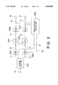
- FIG. 1 is a block diagram of a conventional phase shift circuit
- FIG. 2 is a block diagram of a phase shift circuit according to a first embodiment of the present invention
- FIG. 3 is a graph for showing amplitude ratio dependency of phase difference and amplitude ratio between the output signals in the phase shift circuit of FIG. 2;
- FIG. 4 is a block diagram of a phase shift circuit according to a second embodiment of the present invention.
- a phase shift circuit comprises an CR-RC phase shifter PSI for receiving an input signal through an input terminal 15 to deliver a pair of output signals 11 and 12 having a substantially 900 phase difference therebetween and a substantially equal amplitude, first and second variable-gain amplifiers AM2 and AM3 for amplifying the pair of signals 11 and 12, respectively, with variable gains controlled by gain control signals 81 and 82 to deliver amplified signals 21 and 31, respectively, a pair of subtracter SU4 and adder AD5 for receiving the amplified signals 21 and 31, respectively, from the amplifiers AM2 and AM3 to deliver a difference signal 41 and a sum signal 51, respectively, first and second amplitude equalizers EQ6 and EQ7 for clipping the amplitudes of the difference signal 41 and the sum signal 51, respectively, to output amplitude-equalized signals 61 and 71 through output terminals 16 and 17, respectively, and a phase error detector PD8 for detecting a phase difference or phase error between the
- Phase shifter PS1 may be implemented by a CR-RC phase shifter pair comprising a first CR circuit having a first capacitor inserted between the input 15 and the first output 11 of the phase shifter PSI and a first resistor connected between the first output 11 and the ground, and a second CR circuit having a second resistor inserted between the input 15 and the second output 12 of the phase shifter PS1 and a second capacitor connected between the second output 12 and the ground.
- the amplitude equalizers EQ6 and EQ7 may be implemented by a pair of nonlinear amplifiers having equal characteristics to clip the amplitudes of the difference signal 41 and the sum signal 51, respectively.
- the pair of output signals 11 and 12 from the phase shifter PS1 are expressed by a ⁇ cos ⁇ t and sin( ⁇ t+ ⁇ ), wherein "a” represents amplitude ratio between the signals 11 and 12 and ⁇ is a phase error deviated from 90° in the phase difference between the signals 11 and 12.
- the sum signal 51 (S 51 ) output from the adder AD5 is expressed by: ##EQU2## wherein "k” represents the ratio between the gains by the variable-gain amplifiers AM2 and AM3, and
- Phase difference ⁇ between the sum signal 51 and the difference signal 41 is expressed by:
- FIG. 3 shows gain ratio (k) dependency of the phase difference ⁇ (degrees) and amplitude ratio ⁇ V (dB), wherein 201 ogk (dB) is plotted on abscissa and both phase difference ( ⁇ ) in degrees and amplitude ratio ( ⁇ V) in decibel are plotted on ordinate.
- the phase error detector PD8 detects phase difference ( ⁇ ) between the outputs 61 and 71 from the equalizers EQ6 and EQ7 which clip the amplitude of the output 51 from the adder AD5 and the amplitude of the output 41 from the subtracter SU4 to equalize the amplitudes of the signals 61 and 71.
- the detected phase difference ( ⁇ ) is converted to amplitude control signals 81 and 82 having a ratio of "k" therebetween, which is specified by the graph in FIG. 2.
- the amplitude control signals 81 and 82 are fed-back to the variable gain amplifiers AM2 and AM3, wherein the gains for the amplification are controlled based on the amplitude control signals 81 and 82 to obtain output signals 61 and 71 having an accurate phase difference of 90° therebetween.
- the amplitude control signals 81 and 82 fed-back to the variable-gain amplifiers AM2 and AM3 include a component caused by the phase error; and accordingly, allows the phase shift circuit of the present embodiment to output a pair of output signals 61 and 71 having a correct phase difference of 90° therebetween and an equal amplitude.
- a phase shift circuit according to a second embodiment of the present invention is similar to the first embodiment except that a pair of variable-gain amplifiers AM2 and AM3 receiving the gain control signals 81 and 82 from the phase error detector PD8 are disposed for receiving the input signal through the input terminal 15 to deliver the amplified signals to the CR-RC phase shifter PS1 including a pair of CR phase shift elements, wherein the amplified signals 21 and 31 are subjected to phase shift to have a phase difference of 90° therebetween.
- the outputs 11 and 12 of the phase shifter PS1 are delivered to the adder AD5 and the subtracter SU4.
- Other configuration of the present embodiment is similar to the configuration of the first embodiment.
- the sum signal (S 51 ) 51 output from the adder AD5 and the difference signal (D 41 ) 41 output from the subtracter SU4 are expressed by:
- phase difference ( ⁇ ) between the sum signal 51 and the difference signal 41 and phase ratio ⁇ V are expressed by:
- the amplitude error can be corrected by provision of the variable-gain amplifiers receiving the gain control signals generated based on the phase difference between the output carrier signals.
- the phase shift circuit is preferably used for obtaining a pair of high frequency carrier signals in a communication system.
Abstract
Description
sin(ΔΦ)/cos(ΔΦ)=tan(ΔΦ) (3).
tamΦ.sub.A =ka/cos(ΔΦ)+tan(ΔΦ)
Φ=Φ.sub.A -Φ.sub.S =tan.sup.-1 {ka/cos(ΔΦ)+tan(ΔΦ)}-tan.sup.-1 {-ka/cos(ΔΦ)+tan(ΔΦ)} (6)
ΔV=[cos.sup.2 (ΔΦ)+{ka+sin(ΔΦ)}.sup.2 ].sup.1/2 /[cos.sup.2 (ΔΦ)+{ka-sin(ΔΦ)}.sup.2 ].sup.1/2(7)
S.sub.51 =[cos.sup.2 (ΔΦ)+{ka+sin(ΔΦ)}.sup.2 ].sup.1/2 ·sin(ωt+Φ.sub.A),
D.sub.41 =[cos.sup.2 (ΔΦ)+{ka-sin(ΔΦ)}.sup.2 ].sup.1/2 ·sin(ωt+Φ.sub.S).
Φ=tan.sup.-1 {ka/cos(ΔΦ)+tan(ΔΦ)}-tan.sup.-1 {-ka/cos(ΔΦ)+tan(ΔΦ),
ΔV=[cos.sup.2 (ΔΦ)+{ka+sin(ΔΦ)}.sup.2 ].sup.1/2 /[cos.sup.2 (ΔΦ)+{ka-sin(ΔΦ)}.sup.2 ].sup.1/2.
Claims (6)
Applications Claiming Priority (2)
| Application Number | Priority Date | Filing Date | Title |
|---|---|---|---|
| JP09170402A JP3098464B2 (en) | 1997-06-26 | 1997-06-26 | 90 degree phase shift circuit |
| JP9-170402 | 1997-06-26 |
Publications (1)
| Publication Number | Publication Date |
|---|---|
| US6054883A true US6054883A (en) | 2000-04-25 |
Family
ID=15904270
Family Applications (1)
| Application Number | Title | Priority Date | Filing Date |
|---|---|---|---|
| US09/104,107 Expired - Lifetime US6054883A (en) | 1997-06-26 | 1998-06-25 | High accuracy 90° phase shift circuit error detection |
Country Status (2)
| Country | Link |
|---|---|
| US (1) | US6054883A (en) |
| JP (1) | JP3098464B2 (en) |
Cited By (10)
| Publication number | Priority date | Publication date | Assignee | Title |
|---|---|---|---|---|
| US6340908B1 (en) * | 1999-04-21 | 2002-01-22 | Sony Corporation | Phase adjusting circuit, scaling signal generation circuit using phase adjusting circuit, and position measuring apparatus using scaling signal generation circuit |
| US6356131B1 (en) * | 1999-10-19 | 2002-03-12 | Nec Corporation | 90-degree phase shifter |
| US6396328B2 (en) * | 1999-12-16 | 2002-05-28 | General Research Of Electronics Inc. | Variable capacitance circuit |
| WO2002065638A1 (en) * | 2001-02-12 | 2002-08-22 | Koninklijke Philips Electronics N.V. | Tunable quadrature phase shifter |
| WO2003017483A1 (en) * | 2001-08-16 | 2003-02-27 | Koninklijke Philips Electronics N.V. | Tunable quadrature phase shifter |
| US20080238515A1 (en) * | 2007-03-26 | 2008-10-02 | Kim Hyun-Seok | Signal generation apparatus for frequency conversion in communication system |
| CN1925051B (en) * | 2005-08-30 | 2010-08-25 | 国际商业机器公司 | Read channel and memory driver for dynamically adapting a read channel equalizer |
| US20130038351A1 (en) * | 2011-08-09 | 2013-02-14 | National Semiconductor Corporation | Phase detector |
| US8942621B2 (en) | 2010-03-29 | 2015-01-27 | Asahi Kasei Microdevices Corporation | Phase adjustment circuit and phase adjustment method |
| EP3055927B1 (en) * | 2013-10-11 | 2017-10-04 | Telefonaktiebolaget LM Ericsson (publ) | Signal generator and associated phase shift apparatus and method |
Families Citing this family (10)
| Publication number | Priority date | Publication date | Assignee | Title |
|---|---|---|---|---|
| KR100465912B1 (en) * | 2002-07-30 | 2005-01-13 | 한국과학기술원 | Quadrature signal generator |
| JP2007104007A (en) * | 2005-09-30 | 2007-04-19 | Toshiba Corp | Orthogonal modulator, and vector correction method in the same |
| TW200816661A (en) * | 2006-09-25 | 2008-04-01 | Alcor Micro Corp | Method for I/Q signal adjustment |
| JP2010016702A (en) * | 2008-07-04 | 2010-01-21 | Mitsubishi Electric Corp | High frequency circuit |
| KR20110024236A (en) * | 2009-09-01 | 2011-03-09 | 삼성전자주식회사 | Method and circuit for calibrating phase, and signal processing apparatus having the same |
| JP5582986B2 (en) * | 2010-09-22 | 2014-09-03 | シチズンホールディングス株式会社 | Proximity sensor |
| JP5834577B2 (en) * | 2011-07-21 | 2015-12-24 | 株式会社リコー | Orthogonal signal generation circuit, method for adjusting orthogonal signal generation circuit, and wireless communication apparatus |
| CN102960451A (en) * | 2012-11-29 | 2013-03-13 | 吴柠君 | Sakura strawberry milk and producing method thereof |
| WO2017149699A1 (en) * | 2016-03-02 | 2017-09-08 | 三菱電機株式会社 | Phase shift precision calibration circuit, vector synthesis phase shifter, and wireless communication device |
| WO2022249426A1 (en) * | 2021-05-28 | 2022-12-01 | 三菱電機株式会社 | Phase detection circuit |
Citations (6)
| Publication number | Priority date | Publication date | Assignee | Title |
|---|---|---|---|---|
| US4109102A (en) * | 1975-12-02 | 1978-08-22 | Nippon Electric Company, Ltd. | Phase synchronizing circuit |
| JPH05110369A (en) * | 1991-09-02 | 1993-04-30 | American Teleph & Telegr Co <Att> | Phase shifter |
| JPH06283966A (en) * | 1993-03-30 | 1994-10-07 | Toshiba Corp | Pi/2 phase control circuit |
| JPH07303028A (en) * | 1994-05-09 | 1995-11-14 | Hitachi Ltd | 90× phase shift circuit |
| JPH0818397A (en) * | 1994-06-27 | 1996-01-19 | Hitachi Ltd | 90-degree phase shifter |
| US5886584A (en) * | 1996-05-31 | 1999-03-23 | Ando Electric Co., Ltd. | Method and apparatus for adjusting modulation accuracy of an orthogonal modulation |
-
1997
- 1997-06-26 JP JP09170402A patent/JP3098464B2/en not_active Expired - Fee Related
-
1998
- 1998-06-25 US US09/104,107 patent/US6054883A/en not_active Expired - Lifetime
Patent Citations (6)
| Publication number | Priority date | Publication date | Assignee | Title |
|---|---|---|---|---|
| US4109102A (en) * | 1975-12-02 | 1978-08-22 | Nippon Electric Company, Ltd. | Phase synchronizing circuit |
| JPH05110369A (en) * | 1991-09-02 | 1993-04-30 | American Teleph & Telegr Co <Att> | Phase shifter |
| JPH06283966A (en) * | 1993-03-30 | 1994-10-07 | Toshiba Corp | Pi/2 phase control circuit |
| JPH07303028A (en) * | 1994-05-09 | 1995-11-14 | Hitachi Ltd | 90× phase shift circuit |
| JPH0818397A (en) * | 1994-06-27 | 1996-01-19 | Hitachi Ltd | 90-degree phase shifter |
| US5886584A (en) * | 1996-05-31 | 1999-03-23 | Ando Electric Co., Ltd. | Method and apparatus for adjusting modulation accuracy of an orthogonal modulation |
Cited By (17)
| Publication number | Priority date | Publication date | Assignee | Title |
|---|---|---|---|---|
| US6340908B1 (en) * | 1999-04-21 | 2002-01-22 | Sony Corporation | Phase adjusting circuit, scaling signal generation circuit using phase adjusting circuit, and position measuring apparatus using scaling signal generation circuit |
| US6356131B1 (en) * | 1999-10-19 | 2002-03-12 | Nec Corporation | 90-degree phase shifter |
| US6396328B2 (en) * | 1999-12-16 | 2002-05-28 | General Research Of Electronics Inc. | Variable capacitance circuit |
| WO2002065638A1 (en) * | 2001-02-12 | 2002-08-22 | Koninklijke Philips Electronics N.V. | Tunable quadrature phase shifter |
| US20020158678A1 (en) * | 2001-02-12 | 2002-10-31 | Sanduleanu Mihai Adrian Tiberiu | Tunable quadrature phase shifter |
| US6873198B2 (en) | 2001-02-12 | 2005-03-29 | Mihai Adrian Tiberiu Sanduleanu | Tunable quadrature phase shifter |
| WO2003017483A1 (en) * | 2001-08-16 | 2003-02-27 | Koninklijke Philips Electronics N.V. | Tunable quadrature phase shifter |
| US6747499B2 (en) | 2001-08-16 | 2004-06-08 | Koninklijke Philips Electronics N.V. | Tunable quadrature phase shifter using an all-pass circuit |
| CN1541448B (en) * | 2001-08-16 | 2010-11-24 | Nxp股份有限公司 | Tunable quadrature phase shifter |
| CN1925051B (en) * | 2005-08-30 | 2010-08-25 | 国际商业机器公司 | Read channel and memory driver for dynamically adapting a read channel equalizer |
| US20080238515A1 (en) * | 2007-03-26 | 2008-10-02 | Kim Hyun-Seok | Signal generation apparatus for frequency conversion in communication system |
| US7633325B2 (en) * | 2007-03-26 | 2009-12-15 | Samsung Electronics Co., Ltd. | Signal generation apparatus for frequency conversion in communication system |
| US8942621B2 (en) | 2010-03-29 | 2015-01-27 | Asahi Kasei Microdevices Corporation | Phase adjustment circuit and phase adjustment method |
| EP2555483A4 (en) * | 2010-03-29 | 2017-06-28 | Asahi Kasei Microdevices Corporation | Phase adjustment circuit and phase adjustment method |
| US20130038351A1 (en) * | 2011-08-09 | 2013-02-14 | National Semiconductor Corporation | Phase detector |
| US9030236B2 (en) * | 2011-08-09 | 2015-05-12 | National Semiconductor Corporation | Phase detector |
| EP3055927B1 (en) * | 2013-10-11 | 2017-10-04 | Telefonaktiebolaget LM Ericsson (publ) | Signal generator and associated phase shift apparatus and method |
Also Published As
| Publication number | Publication date |
|---|---|
| JPH1117757A (en) | 1999-01-22 |
| JP3098464B2 (en) | 2000-10-16 |
Similar Documents
| Publication | Publication Date | Title |
|---|---|---|
| US6054883A (en) | High accuracy 90° phase shift circuit error detection | |
| US8792545B2 (en) | Balancing amplitude and phase | |
| US5802451A (en) | Non-linear compensation circuit for a power amplifier | |
| JP3340341B2 (en) | Level identification circuit | |
| US7196579B2 (en) | Gain-controlled amplifier, receiver circuit and radio communication device | |
| US7598805B2 (en) | Load insensitive balanced power amplifier and related operating method | |
| WO2001082473A1 (en) | Distortion compensation apparatus | |
| US5533064A (en) | Digital radio receiver having limiter amplifiers and logarithmic detector | |
| US5521548A (en) | Phase detector | |
| JPH1022758A (en) | Temperature compensated power detection circuit of wide operation range for portable rf transmission terminal equipment | |
| US8670728B2 (en) | Phase correction apparatus and phase correction method | |
| US4742565A (en) | Radio receiver with field intensity detector | |
| US5628059A (en) | DC offset circuit for cartesian loop | |
| US4054840A (en) | FM demodulator using multiplier to which delayed and undelayed input signals are applied | |
| US11411312B2 (en) | Phase adjusting circuit and phase adjusting method | |
| JP3429395B2 (en) | Adaptive equalizer for analog optical signal transmission | |
| JP3228358B2 (en) | Quadrature phase error compensation circuit | |
| US4172966A (en) | AM stereophonic receiver | |
| US4833340A (en) | Phase shifter | |
| JPH0552084B2 (en) | ||
| JP3420613B2 (en) | Quadrature modulator | |
| US5625321A (en) | Variable gain amplifier apparatus | |
| US6525568B2 (en) | Circuit for the demodulation of the logic signal transmitted by analog channels | |
| US3975699A (en) | Linear roll-off filter network | |
| GB1576684A (en) | Demodulating apparatus |
Legal Events
| Date | Code | Title | Description |
|---|---|---|---|
| AS | Assignment |
Owner name: NEC CORPORATION, JAPAN Free format text: ASSIGNMENT OF ASSIGNORS INTEREST;ASSIGNOR:ISHIHARA, HISAYA;REEL/FRAME:009292/0515 Effective date: 19980619 |
|
| FEPP | Fee payment procedure |
Free format text: PAYOR NUMBER ASSIGNED (ORIGINAL EVENT CODE: ASPN); ENTITY STATUS OF PATENT OWNER: LARGE ENTITY |
|
| STCF | Information on status: patent grant |
Free format text: PATENTED CASE |
|
| AS | Assignment |
Owner name: NEC ELECTRONICS CORPORATION, JAPAN Free format text: ASSIGNMENT OF ASSIGNORS INTEREST;ASSIGNOR:NEC CORPORATION;REEL/FRAME:013751/0721 Effective date: 20021101 |
|
| FPAY | Fee payment |
Year of fee payment: 4 |
|
| AS | Assignment |
Owner name: NEC COMPOUND SEMICONDUCTOR DEVICES, LTD., JAPAN Free format text: ASSIGNMENT OF ASSIGNORS INTEREST;ASSIGNOR:NEC ELECTRONICS CORPORATION;REEL/FRAME:014186/0811 Effective date: 20031101 |
|
| AS | Assignment |
Owner name: NEC ELECTRONICS CORPORATION, JAPAN Free format text: ASSIGNMENT OF ASSIGNORS INTEREST;ASSIGNOR:NEC COMPOUND SEMICONDUCTOR DEVICES, LTD.;REEL/FRAME:017422/0528 Effective date: 20060315 |
|
| FPAY | Fee payment |
Year of fee payment: 8 |
|
| AS | Assignment |
Owner name: RENESAS ELECTRONICS CORPORATION, JAPAN Free format text: CHANGE OF NAME;ASSIGNOR:NEC ELECTRONICS CORPORATION;REEL/FRAME:025183/0574 Effective date: 20100401 |
|
| FPAY | Fee payment |
Year of fee payment: 12 |
|
| AS | Assignment |
Owner name: RENESAS ELECTRONICS CORPORATION, JAPAN Free format text: CHANGE OF ADDRESS;ASSIGNOR:RENESAS ELECTRONICS CORPORATION;REEL/FRAME:044928/0001 Effective date: 20150806 |