US5982003A - Silicon-on-insulator transistors having improved current characteristics and reduced electrostatic discharge susceptibility - Google Patents
Silicon-on-insulator transistors having improved current characteristics and reduced electrostatic discharge susceptibility Download PDFInfo
- Publication number
- US5982003A US5982003A US08/461,355 US46135595A US5982003A US 5982003 A US5982003 A US 5982003A US 46135595 A US46135595 A US 46135595A US 5982003 A US5982003 A US 5982003A
- Authority
- US
- United States
- Prior art keywords
- soi
- silicon
- source
- region
- transistors
- Prior art date
- Legal status (The legal status is an assumption and is not a legal conclusion. Google has not performed a legal analysis and makes no representation as to the accuracy of the status listed.)
- Expired - Fee Related
Links
- 239000012212 insulator Substances 0.000 title claims description 5
- 239000004065 semiconductor Substances 0.000 claims description 6
- 230000005669 field effect Effects 0.000 claims description 4
- 239000000463 material Substances 0.000 claims description 4
- XUIMIQQOPSSXEZ-UHFFFAOYSA-N Silicon Chemical compound [Si] XUIMIQQOPSSXEZ-UHFFFAOYSA-N 0.000 abstract description 39
- 229910052710 silicon Inorganic materials 0.000 abstract description 39
- 239000010703 silicon Substances 0.000 abstract description 39
- 239000010408 film Substances 0.000 abstract description 27
- 239000000758 substrate Substances 0.000 abstract description 18
- 230000004888 barrier function Effects 0.000 abstract description 17
- 239000007943 implant Substances 0.000 abstract description 10
- 239000000969 carrier Substances 0.000 abstract description 7
- 239000002019 doping agent Substances 0.000 abstract description 5
- 238000009413 insulation Methods 0.000 abstract description 2
- 239000010409 thin film Substances 0.000 abstract description 2
- 238000005516 engineering process Methods 0.000 description 14
- 238000004519 manufacturing process Methods 0.000 description 9
- 229910021420 polycrystalline silicon Inorganic materials 0.000 description 9
- 229920005591 polysilicon Polymers 0.000 description 9
- 238000000034 method Methods 0.000 description 8
- 239000000872 buffer Substances 0.000 description 6
- 230000000694 effects Effects 0.000 description 6
- 230000008569 process Effects 0.000 description 6
- VYPSYNLAJGMNEJ-UHFFFAOYSA-N Silicium dioxide Chemical compound O=[Si]=O VYPSYNLAJGMNEJ-UHFFFAOYSA-N 0.000 description 4
- 230000008901 benefit Effects 0.000 description 4
- 238000002955 isolation Methods 0.000 description 4
- 229910052814 silicon oxide Inorganic materials 0.000 description 4
- 230000005641 tunneling Effects 0.000 description 4
- 230000015556 catabolic process Effects 0.000 description 3
- 230000009977 dual effect Effects 0.000 description 3
- 230000010354 integration Effects 0.000 description 3
- 229910021421 monocrystalline silicon Inorganic materials 0.000 description 3
- 150000004767 nitrides Chemical class 0.000 description 3
- 230000003071 parasitic effect Effects 0.000 description 3
- 235000012431 wafers Nutrition 0.000 description 3
- 229910052581 Si3N4 Inorganic materials 0.000 description 2
- 238000005530 etching Methods 0.000 description 2
- 238000010438 heat treatment Methods 0.000 description 2
- 150000002500 ions Chemical class 0.000 description 2
- 229910052751 metal Inorganic materials 0.000 description 2
- 239000002184 metal Substances 0.000 description 2
- 230000009467 reduction Effects 0.000 description 2
- HQVNEWCFYHHQES-UHFFFAOYSA-N silicon nitride Chemical compound N12[Si]34N5[Si]62N3[Si]51N64 HQVNEWCFYHHQES-UHFFFAOYSA-N 0.000 description 2
- 238000012421 spiking Methods 0.000 description 2
- 230000001629 suppression Effects 0.000 description 2
- 230000005856 abnormality Effects 0.000 description 1
- 229910052782 aluminium Inorganic materials 0.000 description 1
- XAGFODPZIPBFFR-UHFFFAOYSA-N aluminium Chemical compound [Al] XAGFODPZIPBFFR-UHFFFAOYSA-N 0.000 description 1
- QVGXLLKOCUKJST-UHFFFAOYSA-N atomic oxygen Chemical compound [O] QVGXLLKOCUKJST-UHFFFAOYSA-N 0.000 description 1
- 239000012141 concentrate Substances 0.000 description 1
- 230000003247 decreasing effect Effects 0.000 description 1
- 230000001934 delay Effects 0.000 description 1
- 238000013461 design Methods 0.000 description 1
- 238000009792 diffusion process Methods 0.000 description 1
- 238000002513 implantation Methods 0.000 description 1
- 230000000873 masking effect Effects 0.000 description 1
- 230000007246 mechanism Effects 0.000 description 1
- 238000002844 melting Methods 0.000 description 1
- 230000008018 melting Effects 0.000 description 1
- 238000001465 metallisation Methods 0.000 description 1
- 238000012986 modification Methods 0.000 description 1
- 230000004048 modification Effects 0.000 description 1
- 230000007935 neutral effect Effects 0.000 description 1
- 229910052760 oxygen Inorganic materials 0.000 description 1
- 239000001301 oxygen Substances 0.000 description 1
- 238000012856 packing Methods 0.000 description 1
- 229920002120 photoresistant polymer Polymers 0.000 description 1
- 238000005036 potential barrier Methods 0.000 description 1
- 238000012545 processing Methods 0.000 description 1
- 238000001953 recrystallisation Methods 0.000 description 1
- 238000011160 research Methods 0.000 description 1
- 229920006395 saturated elastomer Polymers 0.000 description 1
- 238000000926 separation method Methods 0.000 description 1
- 238000012546 transfer Methods 0.000 description 1
- 238000009827 uniform distribution Methods 0.000 description 1
- 238000004857 zone melting Methods 0.000 description 1
Images


Classifications
-
- H—ELECTRICITY
- H01—ELECTRIC ELEMENTS
- H01L—SEMICONDUCTOR DEVICES NOT COVERED BY CLASS H10
- H01L29/00—Semiconductor devices specially adapted for rectifying, amplifying, oscillating or switching and having potential barriers; Capacitors or resistors having potential barriers, e.g. a PN-junction depletion layer or carrier concentration layer; Details of semiconductor bodies or of electrodes thereof ; Multistep manufacturing processes therefor
- H01L29/40—Electrodes ; Multistep manufacturing processes therefor
- H01L29/41—Electrodes ; Multistep manufacturing processes therefor characterised by their shape, relative sizes or dispositions
- H01L29/423—Electrodes ; Multistep manufacturing processes therefor characterised by their shape, relative sizes or dispositions not carrying the current to be rectified, amplified or switched
- H01L29/42312—Gate electrodes for field effect devices
- H01L29/42316—Gate electrodes for field effect devices for field-effect transistors
- H01L29/4232—Gate electrodes for field effect devices for field-effect transistors with insulated gate
- H01L29/42384—Gate electrodes for field effect devices for field-effect transistors with insulated gate for thin film field effect transistors, e.g. characterised by the thickness or the shape of the insulator or the dimensions, the shape or the lay-out of the conductor
-
- H—ELECTRICITY
- H01—ELECTRIC ELEMENTS
- H01L—SEMICONDUCTOR DEVICES NOT COVERED BY CLASS H10
- H01L29/00—Semiconductor devices specially adapted for rectifying, amplifying, oscillating or switching and having potential barriers; Capacitors or resistors having potential barriers, e.g. a PN-junction depletion layer or carrier concentration layer; Details of semiconductor bodies or of electrodes thereof ; Multistep manufacturing processes therefor
- H01L29/66—Types of semiconductor device ; Multistep manufacturing processes therefor
- H01L29/66007—Multistep manufacturing processes
- H01L29/66075—Multistep manufacturing processes of devices having semiconductor bodies comprising group 14 or group 13/15 materials
- H01L29/66227—Multistep manufacturing processes of devices having semiconductor bodies comprising group 14 or group 13/15 materials the devices being controllable only by the electric current supplied or the electric potential applied, to an electrode which does not carry the current to be rectified, amplified or switched, e.g. three-terminal devices
- H01L29/66409—Unipolar field-effect transistors
- H01L29/66477—Unipolar field-effect transistors with an insulated gate, i.e. MISFET
- H01L29/66537—Unipolar field-effect transistors with an insulated gate, i.e. MISFET using a self aligned punch through stopper or threshold implant under the gate region
-
- H—ELECTRICITY
- H01—ELECTRIC ELEMENTS
- H01L—SEMICONDUCTOR DEVICES NOT COVERED BY CLASS H10
- H01L29/00—Semiconductor devices specially adapted for rectifying, amplifying, oscillating or switching and having potential barriers; Capacitors or resistors having potential barriers, e.g. a PN-junction depletion layer or carrier concentration layer; Details of semiconductor bodies or of electrodes thereof ; Multistep manufacturing processes therefor
- H01L29/66—Types of semiconductor device ; Multistep manufacturing processes therefor
- H01L29/66007—Multistep manufacturing processes
- H01L29/66075—Multistep manufacturing processes of devices having semiconductor bodies comprising group 14 or group 13/15 materials
- H01L29/66227—Multistep manufacturing processes of devices having semiconductor bodies comprising group 14 or group 13/15 materials the devices being controllable only by the electric current supplied or the electric potential applied, to an electrode which does not carry the current to be rectified, amplified or switched, e.g. three-terminal devices
- H01L29/66409—Unipolar field-effect transistors
- H01L29/66477—Unipolar field-effect transistors with an insulated gate, i.e. MISFET
- H01L29/66742—Thin film unipolar transistors
- H01L29/66772—Monocristalline silicon transistors on insulating substrates, e.g. quartz substrates
-
- H—ELECTRICITY
- H01—ELECTRIC ELEMENTS
- H01L—SEMICONDUCTOR DEVICES NOT COVERED BY CLASS H10
- H01L29/00—Semiconductor devices specially adapted for rectifying, amplifying, oscillating or switching and having potential barriers; Capacitors or resistors having potential barriers, e.g. a PN-junction depletion layer or carrier concentration layer; Details of semiconductor bodies or of electrodes thereof ; Multistep manufacturing processes therefor
- H01L29/66—Types of semiconductor device ; Multistep manufacturing processes therefor
- H01L29/68—Types of semiconductor device ; Multistep manufacturing processes therefor controllable by only the electric current supplied, or only the electric potential applied, to an electrode which does not carry the current to be rectified, amplified or switched
- H01L29/76—Unipolar devices, e.g. field effect transistors
- H01L29/772—Field effect transistors
- H01L29/78—Field effect transistors with field effect produced by an insulated gate
- H01L29/786—Thin film transistors, i.e. transistors with a channel being at least partly a thin film
- H01L29/78606—Thin film transistors, i.e. transistors with a channel being at least partly a thin film with supplementary region or layer in the thin film or in the insulated bulk substrate supporting it for controlling or increasing the safety of the device
- H01L29/78612—Thin film transistors, i.e. transistors with a channel being at least partly a thin film with supplementary region or layer in the thin film or in the insulated bulk substrate supporting it for controlling or increasing the safety of the device for preventing the kink- or the snapback effect, e.g. discharging the minority carriers of the channel region for preventing bipolar effect
- H01L29/78615—Thin film transistors, i.e. transistors with a channel being at least partly a thin film with supplementary region or layer in the thin film or in the insulated bulk substrate supporting it for controlling or increasing the safety of the device for preventing the kink- or the snapback effect, e.g. discharging the minority carriers of the channel region for preventing bipolar effect with a body contact
-
- H—ELECTRICITY
- H01—ELECTRIC ELEMENTS
- H01L—SEMICONDUCTOR DEVICES NOT COVERED BY CLASS H10
- H01L29/00—Semiconductor devices specially adapted for rectifying, amplifying, oscillating or switching and having potential barriers; Capacitors or resistors having potential barriers, e.g. a PN-junction depletion layer or carrier concentration layer; Details of semiconductor bodies or of electrodes thereof ; Multistep manufacturing processes therefor
- H01L29/66—Types of semiconductor device ; Multistep manufacturing processes therefor
- H01L29/68—Types of semiconductor device ; Multistep manufacturing processes therefor controllable by only the electric current supplied, or only the electric potential applied, to an electrode which does not carry the current to be rectified, amplified or switched
- H01L29/76—Unipolar devices, e.g. field effect transistors
- H01L29/772—Field effect transistors
- H01L29/78—Field effect transistors with field effect produced by an insulated gate
- H01L29/786—Thin film transistors, i.e. transistors with a channel being at least partly a thin film
- H01L29/78606—Thin film transistors, i.e. transistors with a channel being at least partly a thin film with supplementary region or layer in the thin film or in the insulated bulk substrate supporting it for controlling or increasing the safety of the device
- H01L29/78618—Thin film transistors, i.e. transistors with a channel being at least partly a thin film with supplementary region or layer in the thin film or in the insulated bulk substrate supporting it for controlling or increasing the safety of the device characterised by the drain or the source properties, e.g. the doping structure, the composition, the sectional shape or the contact structure
- H01L29/78621—Thin film transistors, i.e. transistors with a channel being at least partly a thin film with supplementary region or layer in the thin film or in the insulated bulk substrate supporting it for controlling or increasing the safety of the device characterised by the drain or the source properties, e.g. the doping structure, the composition, the sectional shape or the contact structure with LDD structure or an extension or an offset region or characterised by the doping profile
- H01L29/78624—Thin film transistors, i.e. transistors with a channel being at least partly a thin film with supplementary region or layer in the thin film or in the insulated bulk substrate supporting it for controlling or increasing the safety of the device characterised by the drain or the source properties, e.g. the doping structure, the composition, the sectional shape or the contact structure with LDD structure or an extension or an offset region or characterised by the doping profile the source and the drain regions being asymmetrical
-
- H—ELECTRICITY
- H01—ELECTRIC ELEMENTS
- H01L—SEMICONDUCTOR DEVICES NOT COVERED BY CLASS H10
- H01L29/00—Semiconductor devices specially adapted for rectifying, amplifying, oscillating or switching and having potential barriers; Capacitors or resistors having potential barriers, e.g. a PN-junction depletion layer or carrier concentration layer; Details of semiconductor bodies or of electrodes thereof ; Multistep manufacturing processes therefor
- H01L29/66—Types of semiconductor device ; Multistep manufacturing processes therefor
- H01L29/68—Types of semiconductor device ; Multistep manufacturing processes therefor controllable by only the electric current supplied, or only the electric potential applied, to an electrode which does not carry the current to be rectified, amplified or switched
- H01L29/76—Unipolar devices, e.g. field effect transistors
- H01L29/772—Field effect transistors
- H01L29/78—Field effect transistors with field effect produced by an insulated gate
- H01L29/786—Thin film transistors, i.e. transistors with a channel being at least partly a thin film
- H01L29/78696—Thin film transistors, i.e. transistors with a channel being at least partly a thin film characterised by the structure of the channel, e.g. multichannel, transverse or longitudinal shape, length or width, doping structure, or the overlap or alignment between the channel and the gate, the source or the drain, or the contacting structure of the channel
-
- H—ELECTRICITY
- H01—ELECTRIC ELEMENTS
- H01L—SEMICONDUCTOR DEVICES NOT COVERED BY CLASS H10
- H01L27/00—Devices consisting of a plurality of semiconductor or other solid-state components formed in or on a common substrate
- H01L27/02—Devices consisting of a plurality of semiconductor or other solid-state components formed in or on a common substrate including semiconductor components specially adapted for rectifying, oscillating, amplifying or switching and having potential barriers; including integrated passive circuit elements having potential barriers
- H01L27/12—Devices consisting of a plurality of semiconductor or other solid-state components formed in or on a common substrate including semiconductor components specially adapted for rectifying, oscillating, amplifying or switching and having potential barriers; including integrated passive circuit elements having potential barriers the substrate being other than a semiconductor body, e.g. an insulating body
- H01L27/1203—Devices consisting of a plurality of semiconductor or other solid-state components formed in or on a common substrate including semiconductor components specially adapted for rectifying, oscillating, amplifying or switching and having potential barriers; including integrated passive circuit elements having potential barriers the substrate being other than a semiconductor body, e.g. an insulating body the substrate comprising an insulating body on a semiconductor body, e.g. SOI
- H01L27/1207—Devices consisting of a plurality of semiconductor or other solid-state components formed in or on a common substrate including semiconductor components specially adapted for rectifying, oscillating, amplifying or switching and having potential barriers; including integrated passive circuit elements having potential barriers the substrate being other than a semiconductor body, e.g. an insulating body the substrate comprising an insulating body on a semiconductor body, e.g. SOI combined with devices in contact with the semiconductor body, i.e. bulk/SOI hybrid circuits
Definitions
- This invention relates generally to semiconductor devices, and more particular the invention relates to field effect devices fabricated in silicon-on-insulator structures.
- Silicon-on-insulator (SOI) technology employs a layer of semiconductor material overlying an insulation layer on a supporting bulk wafer.
- the structure can be formed by a number of well-known techniques, such as zone melting and recrystallization (ZMR), separation by implanted oxygen (SIMOX), or Bonded and Etchback (BESOI).
- ZMR zone melting and recrystallization
- SIMOX separation by implanted oxygen
- BESOI Bonded and Etchback
- the structure comprises a film of monocrystalline silicon on a buried layer of silicon oxide in a monocrystalline silicon substrate.
- Field effect transistors such as MOSFETs fabricated in the silicon film of an SOI structure have many advantages over MOSFETs fabricated on the traditional bulk silicon substrates including resistance to short-channel effect, steeper subthreshold slopes, increased current drive, higher packing density, reduced parasitic capacitance, and simpler processing steps.
- the range of SOI applications has been limited due to high cost and inferior crystalline quality of SOI wafers.
- recent advancements in the SOI silicon film quality, buried oxide quality, and manufacturing throughput have opened the door to a multitude of ultra large scale integration (ULSI) applications.
- ULSI ultra large scale integration
- MOSFETs fabricated with SOI technology include non-fully depleted MOSFETs with silicon film thickness greater than the maximum channel depletion width and fully-depleted MOSFETs having silicon film thickness less than the maximum channel depletion width.
- the substrate of an SOI MOSFET is usually electrically floating.
- carriers holes in nMOSFETs and electrons in pMOSFETs
- Extra current will start flowing resulting in a "kink" in the I-V characteristics as shown in FIG. 1. This reduces the achievable gain and dynamic swing in analog circuits, and gives rise to abnormality in the transfer characteristics in digital circuits.
- the channel In a fully-depleted SOI MOSFET, the channel is depleted completely under normal operations.
- the source/channel junction has a lower potential barrier, and the carriers generated by impact ionization have smaller effect on the body and channel potential, thus the "kink" softens.
- the resulting output resistance as illustrated in FIG. 2 is poor, thus making SOI technology less attractive than conventional bulk technology in analog circuits.
- the depletion charge is reduced for a given body doping concentration, leading to a smaller threshold voltage.
- Threshold voltage becomes very sensitive to variations in the silicon film thickness, which makes the fabrication of high performance circuits very difficult. Additionally, the reduction of silicon film thickness in a fully-depleted MOSFET gives rise to high source/drain series resistance which in turn lowers the device operation speed. Silicidation can help improve the series resistance, but it will create mechanical stress and the process is hard to control on thin film silicon.
- One solution to the series resistance problem is to selectively reduce the silicon film thickness over the channel region. However, the resulting recessed region and the polysilicon gate are not automatically aligned. To allow for the possible misalignment, the recessed thin silicon region must be made longer than the gate. This reduces the device performance and density, and results in asymmetrical devices.
- Another problem common to both fully-depleted and non-fully-depleted SOI MOSFETs is the parasitic floating-base lateral bipolar transistor existing in parallel with SOI MOSFETs.
- Band-to-band tunneling generated (GIDL) drain leakage and drain/body junction leakage due to thermal generation are multiplied by the gain of the parasitic bipolar junction transistor, which might be as high as 100.
- Low breakdown voltage and anomalously steep subthreshold slope due to a decreasing threshold voltage has been observed.
- the structure is not compatible with VLSI junction and contact technology such as silicidation.
- ESD electrostatic discharge
- the present invention is directed to providing SOI transistors which overcome or reduce the above problems.
- a low barrier body contact is provided under at least the source of an SOI transistor to collect current generated by impact ionization, junction leakage, and tunneling.
- a P-doped region is provided under the N - source region.
- a side contact can be provided to the underlying current collecting region, or tunneling conduction from the underlying region to the overlying source region can accommodate the collected current.
- thicker source/drain regions are provided with the channel region therebetween recessed to reduce series resistance and increase operating speed of the transistor.
- Transistors with different conduction voltages, V T can be accommodated by the channel thinning and by threshold dopant implant into the channel region.
- Fully-depleted SOI MOSFETs and non-fully-depleted SOI MOSFETs can be integrated on the same chip.
- Fully depleted SOI transistors with recessed channel structures are suitable for digital circuits because of suppression of punch-through and the kink effect.
- Non-fully-depleted SOI MOSFETs with the low barrier body contact are ideal for analog applications, but require a thicker body.
- a self-aligned gate and recessed channel process is provided in accordance with the invention.
- buffer transistors can be fabricated directly in the substrate adjacent to an SOI transistor by first removing the semiconductor film and buried oxide layer. The fundamental problem of thermal isolation due to the buried oxide is thus eliminated.
- the transistor is fabricated in electrically isolated islands or in physically isolated mesas, so that each island or mesa can have at least one conducting filament and absorbs some amount of ESD energy. The total ESD energy is thus spread among the isolated regions, whereas in a bulk SOI transistor the ESD current tents to concentrate at a few hot filaments which can lead to device failure.
- FIG. 1 is a plot of I-V characteristics for a non-fully-depleted SOI device.
- FIG. 2 is a plot of I-V characteristics for a fully-depleted SOI device.
- FIG. 3 is a section view of an SOI MOSFET in accordance with one embodiment of the invention.
- FIG. 4 is a graph illustrating a comparison of performance between conventional and SOI MOSFETs in accordance with the structure of FIG. 3.
- FIG. 5 is a section view of another embodiment of an SOI MOSFET in accordance with the invention.
- FIGS. 6A-6F are section views illustrating the fabrication of a self-aligned recessed channel SOI MOSFET in accordance with the invention.
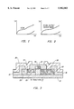
- FIG. 7 is a section view of an SOI MOSFET and a bulk MOSFET for ESD protection in accordance with the invention.
- FIGS. 8 and 9 are graphs illustrating ESD failure voltage of nMOSFETs having different L eff under positive ESD stress.
- FIG. 10 is a plot of ESD failure voltage as a function of channel width.
- FIGS. 11 and 12 are plan views of multiple island ESD production devices in accordance with the invention.
- FIGS. 13 and 14 are plan views of conventional SOI ESD protection devices comprising a single silicon island.
- FIG. 15 is a section view illustrating the fabrication of resistors in the SOI ESD multiple island devices of FIGS. 11 and 12 fabricated in lightly-doped polysilicon films using a light-doped drain implant or source/drain diffusion.
- nMOSFET having a low barrier body contact source region in accordance with the invention is illustrated in cross-section.
- a silicon substrate 10 has a buried silicon oxide layer 12 therein with the transistor fabricated in an overlying monocrystalline silicon film.
- the transistor includes an N + doped drain region 14 and an N + doped source region 16 formed over a P doped body contact 18.
- P + region 20 abutting the source 16 and body contact 18 provides a current path for the impact ionization current accumulated in region 18 near the source/body junction.
- the source region 16 and drain region 14 are separated by a channel region 22 with a polysilicon gate contact 24 overlying the channel region 22 and insulated therefrom by silicon oxide.
- Metal or polysilicon interconnect lines 26, 28 are interconnected with the source and drain, respectively, with the P + region 20 also connected to the source contact line 26.
- the P region 18 underlying the source region provides a low resistance path to collected hole current generated by impact ionization, junction leakage, and GIDL.
- the P implant for the underlying P region 18 is on the order of 1 ⁇ 10 14 to 1 ⁇ 10 16 dopant atoms per cm -2 .
- the N+ implant for the source and drain is higher in dopant concentration with a lower implant energy level to form the shallower N+ doped regions.
- the P- doped low barrier contact can be provided under both the source and drain for a simpler fabrication process.
- the P+ contact 20 is formed after the N+ implant.
- FIG. 4 is a plot illustrating a comparison of performance-between conventional SOI MOSFETs and MOSFETs with the low barrier body contact, as illustrated in FIG. 3.
- the kink effect in non-fully-depleted SOI MOSFETs is completely removed and the bipolar induced problems are suppressed.
- the low barrier body contact MOSFETs exhibit higher breakdown voltage, especially for low gate voltages, and a very constant saturated drain current which is free of the kink.
- the resulting device has all of the advantages of a bulk MOSFET in addition to the better short channel behavior and lower capacitance advantages of SOI structures, which is ideal for analog circuits.
- the low barrier body contact structure in accordance with the invention is capable of collecting carriers uniformly across the channel with a much higher efficiency than the conventional side substrate contact or the mosaic source while requiring less surface area than the conventional schemes.
- Some transistors in a circuit can be designed to have the low barrier body contact structures while others have floating bodies in order to perform pass-gate functions or have the larger current of a floating body MOSFET. Even without the current collection P region (N region for P MOSFETs) beneath the source, the carriers can still be collected by the source if the doping concentration at the bottom of the source is sufficiently low to provide a low barrier for collecting the impact ionization generated carriers.
- FIG. 5 is a section view of another embodiment of the invention in which the P + layer is placed beneath the N + source, and contact is made only to the N + source.
- Like elements in FIGS. 3 and 5 have the same reference numerals.
- the electrical current between the N + and P + regions is carried out by uniform tunneling conduction between the N + and P + silicon as is the well-known mechanism of the operation of a tunnel diode. Even though the N + regions at the source and drain are of different depths, they can be created by the same N + implantation.
- the low barrier body contact is provided only under the source region of the SOI MOSFET.
- a similar low barrier body contact can be provided under the drain region thereby providing a symmetrical transistor structure which is desirable for applications such as a pass-gate circuit.
- FIGS. 6A-6F are section views illustrating a method of fabricating a self-aligned gate and recessed channel structure in accordance with a feature of the invention.
- a substrate (not shown) has a barrier oxide 40 therein with a thicker silicon film 42 thereon.
- a thin layer of silicon oxide 44 is grown on the surface of the silicon film and a layer of silicon nitride 46 is deposited on the oxide layer.
- a window 48 is then etched through the nitride and oxide layers. Thereafter, a sacrificial LOCOS oxide 50 is grown through window 48 into the silicon layer 42 to thin the silicon film where the MOSFET channel will be. An oxide etch is then employed using the nitride layer 46 as a mask to expose the channel region of the silicon film, as shown in FIG. 6C.
- gate oxide is grown on the exposed surface of the silicon film and a polysilicon layer 52 is then formed in the etched hole and over the surface of the silicon nitride.
- the polysilicon film and nitride are removed, leaving the polysilicon gate electrode 53 aligned over the channel region and separated therefrom by the gate oxide from FIG. 6D.
- dopant ions are implanted in the source and drain regions using the gate electrode for self-alignment, oxide 56 is deposited and selectively etched, and metal source and drain interconnect lines 57 and 58 interconnect the transistor structure.
- ultrathin film SOI transistors down to 10 nm can be fabricated using this technique without a problem of the source and drain regions being consumed during contact opening and metallization.
- V T MOSFET threshold voltage
- MOSFETs in a speed-sensitive and leakage-insensitive portion of the circuit can have lower V T while other MOSFETs have a higher V T through use of dual silicon film thickness produced in the recessed channel structure.
- Differences in V T can be controlled by performing threshold adjust implants before or after the LOCOS thinning step (FIG. 6B) and by adjusting the amount of additional uniform thinning after the LOCOS thinning step.
- V T for each of P and N channel transistors can be obtained by masking the V T implant for some transistors with a photoresist mask and using the dual silicon film thickness. Two additional V T can be obtained by implanting P channel threshold adjust ions into N channel transistors, and vice versa for pMOSFETs.
- the use of different silicon film thicknesses on the same chip makes device design very flexible.
- Fully-depleted SOI MOSFETs and non-fully-depleted SOI MOSFETs can be integrated on the same chip with the fully-SOI transistors with a recessed channel structure being particularly useful for digital circuits because of suppression of punch-through and the kink effect.
- Non-fully-depleted SOI MOSFETs with a low barrier body contact are ideal for analog applications but require a thicker body, all of which being accommodated on the same chip in accordance with the invention to give ultimate integration covering a wide range of applications.
- electrostatic discharge (ESD) protection can be incorporated in SOI MOSFET circuits.
- an SOI MOSFET 64 can be fabricated on the oxide layer 68 of substrate 70, while adjacent to transistor 64 a bulk MOSFET 66 is fabricated directly in substrate 70 by etching through the silicon film and buried oxide to create an opening to expose the silicon substrate in which the transistor 66 is fabricated.
- ESD protection circuits including nMOS buffers, pMOS buffers or CMOS buffers can then be fabricated on the silicon substrate at these openings.
- an ESD protection device can be built into the silicon film in thermally isolated segments to increase the ESD current handing capability.
- FIG. 10 is a plot illustrating a special problem of SOI ESD protection, namely, SOI ESD failure voltage does not increase significantly with increasing protection device width. This prevents the attainment of good ESD protection by simply enlarging the device width of an SOI transistor as is routinely done for bulk IC ESD protection.
- the problem lies in the filamentary current flow in the ESD devices under the condition of secondary breakdown. Current is concentrated at hot filaments while cold regions of a transistor carry no current. In a wide bulk transistor, there are many hot spots (filaments) and each filament can absorb certain ESD current or energy without failure.
- the SOI ESD protection device is divided into a plurality of mesas or in silicon islands, each separated by oxide, as illustrated in the plan views of FIGS. 11, 12.
- Each island can have at least one conducting filament and absorb a certain amount of ESD energy so that the 250 ⁇ m-wide SOI device would have about 5 times larger ESD voltage as a 50 ⁇ m-wide device, rather than a similar ESD failure voltage as shown in FIG. 10.
- the use of multiple islands requires little more area than conventional SOI protection devices shown in FIGS. 13 and 14.
- the silicon islands illustrated in FIGS. 11, 12 can be created by field oxide isolation or by physical isolation through etching of mesas.
- the resistors in the subject of FIGS. 11 and 12 can comprise part of a lightly doped drain (LDD) structure as illustrated in FIG. 15 and are added to promote uniform distribution of the ESD current.
- LDD lightly doped drain
- SOI MOSFETs in accordance with the invention improve operating characteristics and speed through use of the low barrier body contact, and the inclusion of non-fully-depleted SOI MOSFETs along with fully-depleted SOI MOSFETs in one SOI integrated circuit can be accommodated using the recessed channel structures along with multiple threshold voltage implants. Further, improved ESD for protection for SOI circuits is readily provided by forming bulk transistors directly in the underlying substrate and through the use of device segmented islands or mesas.
Landscapes
- Engineering & Computer Science (AREA)
- Microelectronics & Electronic Packaging (AREA)
- Power Engineering (AREA)
- Physics & Mathematics (AREA)
- Ceramic Engineering (AREA)
- Condensed Matter Physics & Semiconductors (AREA)
- General Physics & Mathematics (AREA)
- Computer Hardware Design (AREA)
- Manufacturing & Machinery (AREA)
- Thin Film Transistor (AREA)
Abstract
An SOI MOSFET having improved electrical characteristics includes a low barrier body contact under the source region, and alternatively under the drain region, to facilitate collection and removal of current carriers generated by impact ionization. Fully-depleted and non-fully-depleted SOI MOSFETs can be integrated on the same chip by providing some transistors with thicker source and drain regions with a recessed channel therebetween and by selective channel dopant implant. Accordingly, digital circuitry and analog circuitry can be combined on one substrate. Improved electrostatic discharge protection is provided by fabricating transistors for the protection circuit directly in the supporting substrate by first removing the silicon thin film and underlying insulation barrier. Alternatively, improved transistors for electrostatic discharge protection can be formed in the silicon film by fabricating the transistor in a plurality of electrically isolated segments, each segment having source and drain regions separated by a channel region with the regions being electrically interconnected with like regions in other segments. Increased ESD current can be realized as compared to the ESD current for a wider unsegmented device.
Description
This invention was made with Government support under Contract No. F49620-93-C-0014 awarded by the Air Force Office of Scientific Research/Joint Services Electronics Program. The Government has certain rights to this invention.
This is a Division of application Ser. No. 08/224,363, filed Apr. 7, 1994 now U.S. Pat. No. 5,48,9792.
This invention relates generally to semiconductor devices, and more particular the invention relates to field effect devices fabricated in silicon-on-insulator structures.
Silicon-on-insulator (SOI) technology employs a layer of semiconductor material overlying an insulation layer on a supporting bulk wafer. The structure can be formed by a number of well-known techniques, such as zone melting and recrystallization (ZMR), separation by implanted oxygen (SIMOX), or Bonded and Etchback (BESOI). Typically, the structure comprises a film of monocrystalline silicon on a buried layer of silicon oxide in a monocrystalline silicon substrate.
Field effect transistors such as MOSFETs fabricated in the silicon film of an SOI structure have many advantages over MOSFETs fabricated on the traditional bulk silicon substrates including resistance to short-channel effect, steeper subthreshold slopes, increased current drive, higher packing density, reduced parasitic capacitance, and simpler processing steps. In the past, the range of SOI applications has been limited due to high cost and inferior crystalline quality of SOI wafers. However, recent advancements in the SOI silicon film quality, buried oxide quality, and manufacturing throughput have opened the door to a multitude of ultra large scale integration (ULSI) applications. Combined with the continually increasing cost of bulk silicon submicron integrated circuit processes and the lower complexity/cost of SOI integrated circuit processes, SOI technology shows great potential to become the low cost mainstream production technology.
Despite all of the attractiveness of SOI technology, there are obstacles which cancel part of the benefit of using SOI for high-performance, high-density ULSI circuits. The problem is especially severe for analog circuits or mixed-mode circuits, which contain both analog and digital circuits.
MOSFETs fabricated with SOI technology include non-fully depleted MOSFETs with silicon film thickness greater than the maximum channel depletion width and fully-depleted MOSFETs having silicon film thickness less than the maximum channel depletion width. Unlike bulk silicon MOSFETs, the substrate of an SOI MOSFET is usually electrically floating. In a non-fully depleted MOSFET, carriers (holes in nMOSFETs and electrons in pMOSFETs) generated by impact ionization accumulate near the source/body junction of the MOS transistor, and eventually sufficient carriers will accumulate to forward bias the body with respect to the source thus lowering the threshold voltage through the body-bias effect. Extra current will start flowing resulting in a "kink" in the I-V characteristics as shown in FIG. 1. This reduces the achievable gain and dynamic swing in analog circuits, and gives rise to abnormality in the transfer characteristics in digital circuits.
In a fully-depleted SOI MOSFET, the channel is depleted completely under normal operations. The source/channel junction has a lower potential barrier, and the carriers generated by impact ionization have smaller effect on the body and channel potential, thus the "kink" softens. But the resulting output resistance as illustrated in FIG. 2 is poor, thus making SOI technology less attractive than conventional bulk technology in analog circuits.
Furthermore, in fully-depleted MOSFETs, the depletion charge is reduced for a given body doping concentration, leading to a smaller threshold voltage.
Threshold voltage becomes very sensitive to variations in the silicon film thickness, which makes the fabrication of high performance circuits very difficult. Additionally, the reduction of silicon film thickness in a fully-depleted MOSFET gives rise to high source/drain series resistance which in turn lowers the device operation speed. Silicidation can help improve the series resistance, but it will create mechanical stress and the process is hard to control on thin film silicon. One solution to the series resistance problem is to selectively reduce the silicon film thickness over the channel region. However, the resulting recessed region and the polysilicon gate are not automatically aligned. To allow for the possible misalignment, the recessed thin silicon region must be made longer than the gate. This reduces the device performance and density, and results in asymmetrical devices.
Another problem common to both fully-depleted and non-fully-depleted SOI MOSFETs is the parasitic floating-base lateral bipolar transistor existing in parallel with SOI MOSFETs. Band-to-band tunneling generated (GIDL) drain leakage and drain/body junction leakage due to thermal generation are multiplied by the gain of the parasitic bipolar junction transistor, which might be as high as 100. Low breakdown voltage and anomalously steep subthreshold slope due to a decreasing threshold voltage has been observed.
Problems due to the floating body can be solved by providing a contact to the body for hole current collection. However, the currently available hole collection schemes, including the use of a side-contact or the use of a mosaic source are very inefficient and consume significant amounts of device area. A dual source structure has been proposed which depends on an aluminum spiking phenomenon to make contact to the P region, which is sensitive to process variations.
Further, the structure is not compatible with VLSI junction and contact technology such as silicidation.
Another major obstacle to the use of SOI technology in production is electrostatic discharge (ESD) susceptibility. In bulk-substrate technology, good ESD protection levels have been demonstrated by using nMOS/CMOS buffers. However, this protection scheme is not compatible with SOI structures. For example, thick-field-oxide devices are not available on an SOI substrate. Large-area low-series-resistance (vertical) PN junctions are not available as the silicon film can be thinner than 100nm. Experimental results demonstrate that ESD performance on SOI wafers are much worse than bulk technology. This can be due to two reasons, namely the poor thermal conductivity of the buried oxide enhances the failure due to Joule heating, and the reduction of silicon film thickness and junction depth increases the ESD current density. Severe localized silicon heating can result, which causes junction melting and polysilicon melt filaments to form, which cause electrical shorts among the gate, source, drain and body of the transistors and result in device failure. ESD protection schemes designed for SOI circuits have been proposed using additional circuits constructed with diodes and polysilicon resistors, however these devices consume large silicon area, introduce large delays, and are far from adequate.
The present invention is directed to providing SOI transistors which overcome or reduce the above problems.
Briefly, in accordance with the invention, a low barrier body contact is provided under at least the source of an SOI transistor to collect current generated by impact ionization, junction leakage, and tunneling. For an nMOSFET, a P-doped region is provided under the N- source region. A side contact can be provided to the underlying current collecting region, or tunneling conduction from the underlying region to the overlying source region can accommodate the collected current.
In accordance with another feature of the invention, thicker source/drain regions are provided with the channel region therebetween recessed to reduce series resistance and increase operating speed of the transistor. Transistors with different conduction voltages, VT, can be accommodated by the channel thinning and by threshold dopant implant into the channel region. Thus, fully-depleted SOI MOSFETs and non-fully-depleted SOI MOSFETs can be integrated on the same chip. Fully depleted SOI transistors with recessed channel structures are suitable for digital circuits because of suppression of punch-through and the kink effect. Non-fully-depleted SOI MOSFETs with the low barrier body contact are ideal for analog applications, but require a thicker body.
Both analog and digital transistors can thus be accommodated on the same chip giving ultimate integration for a wide range of circuit applications. A self-aligned gate and recessed channel process is provided in accordance with the invention.
To provide electrostatic discharge (ESD) protection, buffer transistors can be fabricated directly in the substrate adjacent to an SOI transistor by first removing the semiconductor film and buried oxide layer. The fundamental problem of thermal isolation due to the buried oxide is thus eliminated. In an alternative embodiment using an SOI transistor for ESD protection, the transistor is fabricated in electrically isolated islands or in physically isolated mesas, so that each island or mesa can have at least one conducting filament and absorbs some amount of ESD energy. The total ESD energy is thus spread among the isolated regions, whereas in a bulk SOI transistor the ESD current tents to concentrate at a few hot filaments which can lead to device failure.
The invention and objects and features thereof will be more fully understood from the following detailed description and appended claims when taken with the drawing.
FIG. 1 is a plot of I-V characteristics for a non-fully-depleted SOI device.
FIG. 2 is a plot of I-V characteristics for a fully-depleted SOI device.
FIG. 3 is a section view of an SOI MOSFET in accordance with one embodiment of the invention.
FIG. 4 is a graph illustrating a comparison of performance between conventional and SOI MOSFETs in accordance with the structure of FIG. 3.
FIG. 5 is a section view of another embodiment of an SOI MOSFET in accordance with the invention.
FIGS. 6A-6F are section views illustrating the fabrication of a self-aligned recessed channel SOI MOSFET in accordance with the invention.
FIG. 7 is a section view of an SOI MOSFET and a bulk MOSFET for ESD protection in accordance with the invention.
FIGS. 8 and 9 are graphs illustrating ESD failure voltage of nMOSFETs having different Leff under positive ESD stress.
FIG. 10 is a plot of ESD failure voltage as a function of channel width.
FIGS. 11 and 12 are plan views of multiple island ESD production devices in accordance with the invention.
FIGS. 13 and 14 are plan views of conventional SOI ESD protection devices comprising a single silicon island.
FIG. 15 is a section view illustrating the fabrication of resistors in the SOI ESD multiple island devices of FIGS. 11 and 12 fabricated in lightly-doped polysilicon films using a light-doped drain implant or source/drain diffusion.
Features of the invention will be described with reference to specific nMOSFET embodiments, but it will be appreciated that the invention applies to pMOSFETs as well.
Referring to FIG. 3, an nMOSFET having a low barrier body contact source region in accordance with the invention is illustrated in cross-section. As in a typical SIMOX structure, a silicon substrate 10 has a buried silicon oxide layer 12 therein with the transistor fabricated in an overlying monocrystalline silicon film. The transistor includes an N+ doped drain region 14 and an N+ doped source region 16 formed over a P doped body contact 18. P+ region 20 abutting the source 16 and body contact 18 provides a current path for the impact ionization current accumulated in region 18 near the source/body junction. The source region 16 and drain region 14 are separated by a channel region 22 with a polysilicon gate contact 24 overlying the channel region 22 and insulated therefrom by silicon oxide. Metal or polysilicon interconnect lines 26, 28 are interconnected with the source and drain, respectively, with the P+ region 20 also connected to the source contact line 26.
The P region 18 underlying the source region, either neutral or depleted, provides a low resistance path to collected hole current generated by impact ionization, junction leakage, and GIDL. The P implant for the underlying P region 18 is on the order of 1×10¹⁴ to 1×10¹⁶ dopant atoms per cm-2. The N+ implant for the source and drain is higher in dopant concentration with a lower implant energy level to form the shallower N+ doped regions. The P- doped low barrier contact can be provided under both the source and drain for a simpler fabrication process. The P+ contact 20 is formed after the N+ implant.
FIG. 4 is a plot illustrating a comparison of performance-between conventional SOI MOSFETs and MOSFETs with the low barrier body contact, as illustrated in FIG. 3. The kink effect in non-fully-depleted SOI MOSFETs is completely removed and the bipolar induced problems are suppressed. The low barrier body contact MOSFETs exhibit higher breakdown voltage, especially for low gate voltages, and a very constant saturated drain current which is free of the kink. The resulting device has all of the advantages of a bulk MOSFET in addition to the better short channel behavior and lower capacitance advantages of SOI structures, which is ideal for analog circuits.
The low barrier body contact structure in accordance with the invention is capable of collecting carriers uniformly across the channel with a much higher efficiency than the conventional side substrate contact or the mosaic source while requiring less surface area than the conventional schemes. Some transistors in a circuit can be designed to have the low barrier body contact structures while others have floating bodies in order to perform pass-gate functions or have the larger current of a floating body MOSFET. Even without the current collection P region (N region for P MOSFETs) beneath the source, the carriers can still be collected by the source if the doping concentration at the bottom of the source is sufficiently low to provide a low barrier for collecting the impact ionization generated carriers.
FIG. 5 is a section view of another embodiment of the invention in which the P+ layer is placed beneath the N+ source, and contact is made only to the N+ source. Like elements in FIGS. 3 and 5 have the same reference numerals. Instead of relying on the non-uniform, therefore uncontrolled, spiking of contact, the electrical current between the N+ and P+ regions is carried out by uniform tunneling conduction between the N+ and P+ silicon as is the well-known mechanism of the operation of a tunnel diode. Even though the N+ regions at the source and drain are of different depths, they can be created by the same N+ implantation.
In the embodiments of FIGS. 3 and 5, the low barrier body contact is provided only under the source region of the SOI MOSFET. However, a similar low barrier body contact can be provided under the drain region thereby providing a symmetrical transistor structure which is desirable for applications such as a pass-gate circuit.
In accordance with another feature of the invention, a thicker film of silicon is employed for the source and drain regions to reduce series source/drain resistance and increase operation speed. Further, non-fully-depleted SOI MOSFETs require a thicker body. However, the thicker source and drain regions require a thinning of the channel region therebetween. FIGS. 6A-6F are section views illustrating a method of fabricating a self-aligned gate and recessed channel structure in accordance with a feature of the invention. In FIG. 6A a substrate (not shown) has a barrier oxide 40 therein with a thicker silicon film 42 thereon. A thin layer of silicon oxide 44 is grown on the surface of the silicon film and a layer of silicon nitride 46 is deposited on the oxide layer. A window 48 is then etched through the nitride and oxide layers. Thereafter, a sacrificial LOCOS oxide 50 is grown through window 48 into the silicon layer 42 to thin the silicon film where the MOSFET channel will be. An oxide etch is then employed using the nitride layer 46 as a mask to expose the channel region of the silicon film, as shown in FIG. 6C. In FIG. 6D, gate oxide is grown on the exposed surface of the silicon film and a polysilicon layer 52 is then formed in the etched hole and over the surface of the silicon nitride. In FIG. 6E, the polysilicon film and nitride are removed, leaving the polysilicon gate electrode 53 aligned over the channel region and separated therefrom by the gate oxide from FIG. 6D. Finally, in FIG. 6F, dopant ions are implanted in the source and drain regions using the gate electrode for self-alignment, oxide 56 is deposited and selectively etched, and metal source and drain interconnect lines 57 and 58 interconnect the transistor structure. In addition to the thicker source/drain regions which can be provided, ultrathin film SOI transistors down to 10 nm can be fabricated using this technique without a problem of the source and drain regions being consumed during contact opening and metallization.
Circuit operating voltage must be reduced in order to reduce power consumption. When the operating voltage is lowered, the MOSFET threshold voltage (VT) must be lowered in order to obtain larger currents and higher circuit speed. Unfortunately, a low VT leads to large transistor leakage, which increases power consumption. By using the low barrier body contact and recessed channel structure of the invention, MOSFETs in a speed-sensitive and leakage-insensitive portion of the circuit can have lower VT while other MOSFETs have a higher VT through use of dual silicon film thickness produced in the recessed channel structure. Differences in VT can be controlled by performing threshold adjust implants before or after the LOCOS thinning step (FIG. 6B) and by adjusting the amount of additional uniform thinning after the LOCOS thinning step. Different VT for each of P and N channel transistors can be obtained by masking the VT implant for some transistors with a photoresist mask and using the dual silicon film thickness. Two additional VT can be obtained by implanting P channel threshold adjust ions into N channel transistors, and vice versa for pMOSFETs. The use of different silicon film thicknesses on the same chip makes device design very flexible. Fully-depleted SOI MOSFETs and non-fully-depleted SOI MOSFETs can be integrated on the same chip with the fully-SOI transistors with a recessed channel structure being particularly useful for digital circuits because of suppression of punch-through and the kink effect. Non-fully-depleted SOI MOSFETs with a low barrier body contact are ideal for analog applications but require a thicker body, all of which being accommodated on the same chip in accordance with the invention to give ultimate integration covering a wide range of applications.
In accordance with another aspect of the invention, electrostatic discharge (ESD) protection can be incorporated in SOI MOSFET circuits. In accordance with one embodiment shown in cross-section in FIG. 7, an SOI MOSFET 64 can be fabricated on the oxide layer 68 of substrate 70, while adjacent to transistor 64 a bulk MOSFET 66 is fabricated directly in substrate 70 by etching through the silicon film and buried oxide to create an opening to expose the silicon substrate in which the transistor 66 is fabricated. ESD protection circuits including nMOS buffers, pMOS buffers or CMOS buffers can then be fabricated on the silicon substrate at these openings. Accordingly, most of the bulk ESD protection circuits are directly transferred to the SOI technology, thus saving time and effort of developing special circuits for SOI ESD protection. The fundamental problem of thermal isolation due to the buried oxide in SOI technology is eliminated, hence giving more flexibility for building the ESD protection circuits. Experimental results demonstrate that ESD protection circuits built directly in the substrate are capable of withstanding higher ESD discharge voltage during the human-body-model stress compared with ESD protection circuits build on conventional SOI circuits for both positive and negative discharge pulses. For negative discharges, conventional SOI NMOS transistors in the buffer are operated in the so-called transistor-diode mode. The series resistance in this operating mode is too large for SOI technology to provide satisfactory ESD protection. However, with bulk MOSFETs, the negative discharge pulses are absorbed by the large drain-to-substrate diode which can accommodate larger ESD currents. The results are summarized in the plots of FIGS. 8 and 9 which show ESD failure voltage of different nMOSFETs with different Leff under positive ESD stress. The transistors have Weff of 250 μm, Tox of 9 nm, and 2 μm contact-to-gate spacing.
In accordance with another feature of the invention, an ESD protection device can be built into the silicon film in thermally isolated segments to increase the ESD current handing capability. FIG. 10 is a plot illustrating a special problem of SOI ESD protection, namely, SOI ESD failure voltage does not increase significantly with increasing protection device width. This prevents the attainment of good ESD protection by simply enlarging the device width of an SOI transistor as is routinely done for bulk IC ESD protection. The problem lies in the filamentary current flow in the ESD devices under the condition of secondary breakdown. Current is concentrated at hot filaments while cold regions of a transistor carry no current. In a wide bulk transistor, there are many hot spots (filaments) and each filament can absorb certain ESD current or energy without failure. However, in an SOI device, it is unlikely to have multiple hot spots since the temperature in a silicon island tends to be more uniform even in a wide transistor because the thermally-conductive silicon island is surrounded by thermally insulating oxide. In accordance with the invention, the SOI ESD protection device is divided into a plurality of mesas or in silicon islands, each separated by oxide, as illustrated in the plan views of FIGS. 11, 12. Each island can have at least one conducting filament and absorb a certain amount of ESD energy so that the 250 μm-wide SOI device would have about 5 times larger ESD voltage as a 50 μm-wide device, rather than a similar ESD failure voltage as shown in FIG. 10. The use of multiple islands requires little more area than conventional SOI protection devices shown in FIGS. 13 and 14. The silicon islands illustrated in FIGS. 11, 12 can be created by field oxide isolation or by physical isolation through etching of mesas. The resistors in the subject of FIGS. 11 and 12 can comprise part of a lightly doped drain (LDD) structure as illustrated in FIG. 15 and are added to promote uniform distribution of the ESD current.
SOI MOSFETs in accordance with the invention improve operating characteristics and speed through use of the low barrier body contact, and the inclusion of non-fully-depleted SOI MOSFETs along with fully-depleted SOI MOSFETs in one SOI integrated circuit can be accommodated using the recessed channel structures along with multiple threshold voltage implants. Further, improved ESD for protection for SOI circuits is readily provided by forming bulk transistors directly in the underlying substrate and through the use of device segmented islands or mesas.
While the invention has been described with reference to specific embodiments, the description is illustrative of the invention and is not to be construed as limiting the invention. Various modifications and applications may occur to those skilled in the art without departing from the true spirit and scope of the invention as defined by the appended claims.
Claims (2)
1. A silicon-on-insulator field effect transistor for use in an electrostatic discharge protection circuit comprising
an insulating layer,
a semiconductor material layer on said insulating layer,
a plurality of phsically and electrically isolated regions of semiconductor material formed from said semiconductor material region, each isolated region having a source region spaced from a drain region by a channel region,
a first interconnect means for electrically connecting all of said source regions,
a second interconnect means for electrically connecting all of said drain regions, and
a third interconnect means overlying all of said channel regions and functioning as a common gate.
2. The silicon-on-insulator field effect transistor as defined by claim 1 wherein said plurality of electrically isolated regions comprise physically isolated mesa structures.
Priority Applications (3)
| Application Number | Priority Date | Filing Date | Title |
|---|---|---|---|
| US08/461,355 US5982003A (en) | 1994-04-07 | 1995-06-05 | Silicon-on-insulator transistors having improved current characteristics and reduced electrostatic discharge susceptibility |
| US09/393,767 US6121077A (en) | 1994-04-07 | 1999-09-10 | Silicon-on-insulator transistors having improved current characteristics and reduced electrostatic discharge susceptibility |
| US09/632,456 US6300649B1 (en) | 1994-04-07 | 2000-08-04 | Silicon-on-insulator transistors having improved current characteristics and reduced electrostatic discharge susceptibility |
Applications Claiming Priority (2)
| Application Number | Priority Date | Filing Date | Title |
|---|---|---|---|
| US08/224,363 US5489792A (en) | 1994-04-07 | 1994-04-07 | Silicon-on-insulator transistors having improved current characteristics and reduced electrostatic discharge susceptibility |
| US08/461,355 US5982003A (en) | 1994-04-07 | 1995-06-05 | Silicon-on-insulator transistors having improved current characteristics and reduced electrostatic discharge susceptibility |
Related Parent Applications (1)
| Application Number | Title | Priority Date | Filing Date |
|---|---|---|---|
| US08/224,363 Division US5489792A (en) | 1994-04-07 | 1994-04-07 | Silicon-on-insulator transistors having improved current characteristics and reduced electrostatic discharge susceptibility |
Related Child Applications (1)
| Application Number | Title | Priority Date | Filing Date |
|---|---|---|---|
| US09/393,767 Division US6121077A (en) | 1994-04-07 | 1999-09-10 | Silicon-on-insulator transistors having improved current characteristics and reduced electrostatic discharge susceptibility |
Publications (1)
| Publication Number | Publication Date |
|---|---|
| US5982003A true US5982003A (en) | 1999-11-09 |
Family
ID=22840347
Family Applications (4)
| Application Number | Title | Priority Date | Filing Date |
|---|---|---|---|
| US08/224,363 Expired - Lifetime US5489792A (en) | 1994-04-07 | 1994-04-07 | Silicon-on-insulator transistors having improved current characteristics and reduced electrostatic discharge susceptibility |
| US08/461,355 Expired - Fee Related US5982003A (en) | 1994-04-07 | 1995-06-05 | Silicon-on-insulator transistors having improved current characteristics and reduced electrostatic discharge susceptibility |
| US09/393,767 Expired - Fee Related US6121077A (en) | 1994-04-07 | 1999-09-10 | Silicon-on-insulator transistors having improved current characteristics and reduced electrostatic discharge susceptibility |
| US09/632,456 Expired - Fee Related US6300649B1 (en) | 1994-04-07 | 2000-08-04 | Silicon-on-insulator transistors having improved current characteristics and reduced electrostatic discharge susceptibility |
Family Applications Before (1)
| Application Number | Title | Priority Date | Filing Date |
|---|---|---|---|
| US08/224,363 Expired - Lifetime US5489792A (en) | 1994-04-07 | 1994-04-07 | Silicon-on-insulator transistors having improved current characteristics and reduced electrostatic discharge susceptibility |
Family Applications After (2)
| Application Number | Title | Priority Date | Filing Date |
|---|---|---|---|
| US09/393,767 Expired - Fee Related US6121077A (en) | 1994-04-07 | 1999-09-10 | Silicon-on-insulator transistors having improved current characteristics and reduced electrostatic discharge susceptibility |
| US09/632,456 Expired - Fee Related US6300649B1 (en) | 1994-04-07 | 2000-08-04 | Silicon-on-insulator transistors having improved current characteristics and reduced electrostatic discharge susceptibility |
Country Status (1)
| Country | Link |
|---|---|
| US (4) | US5489792A (en) |
Cited By (73)
| Publication number | Priority date | Publication date | Assignee | Title |
|---|---|---|---|---|
| US6063672A (en) * | 1999-02-05 | 2000-05-16 | Lsi Logic Corporation | NMOS electrostatic discharge protection device and method for CMOS integrated circuit |
| US6121077A (en) * | 1994-04-07 | 2000-09-19 | The Regents Of The University Of California | Silicon-on-insulator transistors having improved current characteristics and reduced electrostatic discharge susceptibility |
| US6365463B2 (en) * | 1999-05-21 | 2002-04-02 | Nat Semiconductor Corp | Method for forming a high-precision analog transistor with a low threshold voltage roll-up and a digital transistor with a high threshold voltage roll-up |
| US6426244B2 (en) * | 1999-01-08 | 2002-07-30 | International Business Machines Corporation | Process of forming a thick oxide field effect transistor |
| US6509613B1 (en) | 2001-05-04 | 2003-01-21 | Advanced Micro Devices, Inc. | Self-aligned floating body control for SOI device through leakage enhanced buried oxide |
| US6563172B2 (en) * | 1998-01-13 | 2003-05-13 | Mitsubishi Denki Kabushiki Kaisha | Semiconductor substrate processing method |
| US6593624B2 (en) * | 2001-09-25 | 2003-07-15 | Matrix Semiconductor, Inc. | Thin film transistors with vertically offset drain regions |
| US6677645B2 (en) | 2002-01-31 | 2004-01-13 | International Business Machines Corporation | Body contact MOSFET |
| US20040021137A1 (en) * | 2001-06-18 | 2004-02-05 | Pierre Fazan | Semiconductor device |
| US6867103B1 (en) | 2002-05-24 | 2005-03-15 | Taiwan Semiconductor Manufacturing Company | Method of fabricating an ESD device on SOI |
| US6912150B2 (en) | 2003-05-13 | 2005-06-28 | Lionel Portman | Reference current generator, and method of programming, adjusting and/or operating same |
| US6982918B2 (en) | 2002-04-18 | 2006-01-03 | Pierre Fazan | Data storage device and refreshing method for use with such device |
| US20060006468A1 (en) * | 2002-04-18 | 2006-01-12 | Pierre Fazan | Semiconductor device |
| US7085156B2 (en) | 2003-05-13 | 2006-08-01 | Innovative Silicon S.A. | Semiconductor memory device and method of operating same |
| US7085153B2 (en) | 2003-05-13 | 2006-08-01 | Innovative Silicon S.A. | Semiconductor memory cell, array, architecture and device, and method of operating same |
| US20060176628A1 (en) * | 2005-02-04 | 2006-08-10 | Hisashi Hasegawa | Semiconductor integrated circuit device and method of manufacturing the same |
| US7122863B1 (en) | 2001-05-07 | 2006-10-17 | Advanced Micro Devices, Inc. | SOI device with structure for enhancing carrier recombination and method of fabricating same |
| US7177175B2 (en) | 2003-09-24 | 2007-02-13 | Innovative Silicon S.A. | Low power programming technique for a floating body memory transistor, memory cell, and memory array |
| US7251164B2 (en) | 2004-11-10 | 2007-07-31 | Innovative Silicon S.A. | Circuitry for and method of improving statistical distribution of integrated circuits |
| US7301803B2 (en) | 2004-12-22 | 2007-11-27 | Innovative Silicon S.A. | Bipolar reading technique for a memory cell having an electrically floating body transistor |
| US7301838B2 (en) | 2004-12-13 | 2007-11-27 | Innovative Silicon S.A. | Sense amplifier circuitry and architecture to write data into and/or read from memory cells |
| US7335934B2 (en) | 2003-07-22 | 2008-02-26 | Innovative Silicon S.A. | Integrated circuit device, and method of fabricating same |
| US7355916B2 (en) | 2005-09-19 | 2008-04-08 | Innovative Silicon S.A. | Method and circuitry to generate a reference current for reading a memory cell, and device implementing same |
| US7405982B1 (en) | 1997-04-23 | 2008-07-29 | International Business Machines Corporation | Methods to improve the operation of SOI devices |
| US7476939B2 (en) | 2004-11-04 | 2009-01-13 | Innovative Silicon Isi Sa | Memory cell having an electrically floating body transistor and programming technique therefor |
| US7492632B2 (en) | 2006-04-07 | 2009-02-17 | Innovative Silicon Isi Sa | Memory array having a programmable word length, and method of operating same |
| US7542345B2 (en) | 2006-02-16 | 2009-06-02 | Innovative Silicon Isi Sa | Multi-bit memory cell having electrically floating body transistor, and method of programming and reading same |
| US7542340B2 (en) | 2006-07-11 | 2009-06-02 | Innovative Silicon Isi Sa | Integrated circuit including memory array having a segmented bit line architecture and method of controlling and/or operating same |
| US7606098B2 (en) | 2006-04-18 | 2009-10-20 | Innovative Silicon Isi Sa | Semiconductor memory array architecture with grouped memory cells, and method of controlling same |
| US7606066B2 (en) | 2005-09-07 | 2009-10-20 | Innovative Silicon Isi Sa | Memory cell and memory cell array having an electrically floating body transistor, and methods of operating same |
| US7683430B2 (en) | 2005-12-19 | 2010-03-23 | Innovative Silicon Isi Sa | Electrically floating body memory cell and array, and method of operating or controlling same |
| US7825455B2 (en) | 2000-08-14 | 2010-11-02 | Sandisk 3D Llc | Three terminal nonvolatile memory device with vertical gated diode |
| US7924630B2 (en) | 2008-10-15 | 2011-04-12 | Micron Technology, Inc. | Techniques for simultaneously driving a plurality of source lines |
| US7933140B2 (en) | 2008-10-02 | 2011-04-26 | Micron Technology, Inc. | Techniques for reducing a voltage swing |
| US7933142B2 (en) | 2006-05-02 | 2011-04-26 | Micron Technology, Inc. | Semiconductor memory cell and array using punch-through to program and read same |
| US7947543B2 (en) | 2008-09-25 | 2011-05-24 | Micron Technology, Inc. | Recessed gate silicon-on-insulator floating body device with self-aligned lateral isolation |
| US7957206B2 (en) | 2008-04-04 | 2011-06-07 | Micron Technology, Inc. | Read circuitry for an integrated circuit having memory cells and/or a memory cell array, and method of operating same |
| US8014195B2 (en) | 2008-02-06 | 2011-09-06 | Micron Technology, Inc. | Single transistor memory cell |
| US8064274B2 (en) | 2007-05-30 | 2011-11-22 | Micron Technology, Inc. | Integrated circuit having voltage generation circuitry for memory cell array, and method of operating and/or controlling same |
| US8069377B2 (en) | 2006-06-26 | 2011-11-29 | Micron Technology, Inc. | Integrated circuit having memory array including ECC and column redundancy and method of operating the same |
| US8085594B2 (en) | 2007-06-01 | 2011-12-27 | Micron Technology, Inc. | Reading technique for memory cell with electrically floating body transistor |
| US8139418B2 (en) | 2009-04-27 | 2012-03-20 | Micron Technology, Inc. | Techniques for controlling a direct injection semiconductor memory device |
| US8174881B2 (en) | 2009-11-24 | 2012-05-08 | Micron Technology, Inc. | Techniques for reducing disturbance in a semiconductor device |
| US8189376B2 (en) | 2008-02-08 | 2012-05-29 | Micron Technology, Inc. | Integrated circuit having memory cells including gate material having high work function, and method of manufacturing same |
| US8194487B2 (en) | 2007-09-17 | 2012-06-05 | Micron Technology, Inc. | Refreshing data of memory cells with electrically floating body transistors |
| US8199595B2 (en) | 2009-09-04 | 2012-06-12 | Micron Technology, Inc. | Techniques for sensing a semiconductor memory device |
| US8213226B2 (en) | 2008-12-05 | 2012-07-03 | Micron Technology, Inc. | Vertical transistor memory cell and array |
| US8223574B2 (en) | 2008-11-05 | 2012-07-17 | Micron Technology, Inc. | Techniques for block refreshing a semiconductor memory device |
| US8264041B2 (en) | 2007-01-26 | 2012-09-11 | Micron Technology, Inc. | Semiconductor device with electrically floating body |
| US8310893B2 (en) | 2009-12-16 | 2012-11-13 | Micron Technology, Inc. | Techniques for reducing impact of array disturbs in a semiconductor memory device |
| US8315099B2 (en) | 2009-07-27 | 2012-11-20 | Micron Technology, Inc. | Techniques for providing a direct injection semiconductor memory device |
| US8319294B2 (en) | 2009-02-18 | 2012-11-27 | Micron Technology, Inc. | Techniques for providing a source line plane |
| US8349662B2 (en) | 2007-12-11 | 2013-01-08 | Micron Technology, Inc. | Integrated circuit having memory cell array, and method of manufacturing same |
| US8369177B2 (en) | 2010-03-05 | 2013-02-05 | Micron Technology, Inc. | Techniques for reading from and/or writing to a semiconductor memory device |
| US8411524B2 (en) | 2010-05-06 | 2013-04-02 | Micron Technology, Inc. | Techniques for refreshing a semiconductor memory device |
| US8411513B2 (en) | 2010-03-04 | 2013-04-02 | Micron Technology, Inc. | Techniques for providing a semiconductor memory device having hierarchical bit lines |
| US8416636B2 (en) | 2010-02-12 | 2013-04-09 | Micron Technology, Inc. | Techniques for controlling a semiconductor memory device |
| US8498157B2 (en) | 2009-05-22 | 2013-07-30 | Micron Technology, Inc. | Techniques for providing a direct injection semiconductor memory device |
| US8508994B2 (en) | 2009-04-30 | 2013-08-13 | Micron Technology, Inc. | Semiconductor device with floating gate and electrically floating body |
| US8518774B2 (en) | 2007-03-29 | 2013-08-27 | Micron Technology, Inc. | Manufacturing process for zero-capacitor random access memory circuits |
| US8531878B2 (en) | 2011-05-17 | 2013-09-10 | Micron Technology, Inc. | Techniques for providing a semiconductor memory device |
| US8537610B2 (en) | 2009-07-10 | 2013-09-17 | Micron Technology, Inc. | Techniques for providing a semiconductor memory device |
| US8536628B2 (en) | 2007-11-29 | 2013-09-17 | Micron Technology, Inc. | Integrated circuit having memory cell array including barriers, and method of manufacturing same |
| US8547738B2 (en) | 2010-03-15 | 2013-10-01 | Micron Technology, Inc. | Techniques for providing a semiconductor memory device |
| US8576631B2 (en) | 2010-03-04 | 2013-11-05 | Micron Technology, Inc. | Techniques for sensing a semiconductor memory device |
| US8610217B2 (en) | 2010-12-14 | 2013-12-17 | International Business Machines Corporation | Self-protected electrostatic discharge field effect transistor (SPESDFET), an integrated circuit incorporating the SPESDFET as an input/output (I/O) pad driver and associated methods of forming the SPESDFET and the integrated circuit |
| US8710566B2 (en) | 2009-03-04 | 2014-04-29 | Micron Technology, Inc. | Techniques for forming a contact to a buried diffusion layer in a semiconductor memory device |
| US8748959B2 (en) | 2009-03-31 | 2014-06-10 | Micron Technology, Inc. | Semiconductor memory device |
| US8773933B2 (en) | 2012-03-16 | 2014-07-08 | Micron Technology, Inc. | Techniques for accessing memory cells |
| US20140191319A1 (en) * | 2013-01-04 | 2014-07-10 | GlobalFoundries, Inc. | Finfet compatible diode for esd protection |
| US9478495B1 (en) | 2015-10-26 | 2016-10-25 | Sandisk Technologies Llc | Three dimensional memory device containing aluminum source contact via structure and method of making thereof |
| US9559216B2 (en) | 2011-06-06 | 2017-01-31 | Micron Technology, Inc. | Semiconductor memory device and method for biasing same |
| US9627395B2 (en) | 2015-02-11 | 2017-04-18 | Sandisk Technologies Llc | Enhanced channel mobility three-dimensional memory structure and method of making thereof |
Families Citing this family (117)
| Publication number | Priority date | Publication date | Assignee | Title |
|---|---|---|---|---|
| JPH0888323A (en) * | 1994-09-19 | 1996-04-02 | Nippondenso Co Ltd | Semiconductor integrated circuit device |
| JPH08125152A (en) * | 1994-10-28 | 1996-05-17 | Canon Inc | Semiconductor device, correlation operating unit empolying it, ad converter, da converter, and signal processing system |
| JP3240258B2 (en) * | 1996-03-21 | 2001-12-17 | シャープ株式会社 | Semiconductor device, thin film transistor and method for manufacturing the same, and liquid crystal display device and method for manufacturing the same |
| KR0176202B1 (en) * | 1996-04-09 | 1999-04-15 | 김광호 | Soi transistor and its fabrication method |
| KR100253699B1 (en) * | 1996-06-29 | 2000-05-01 | 김영환 | Soi device and its manufacturing method |
| US5767549A (en) * | 1996-07-03 | 1998-06-16 | International Business Machines Corporation | SOI CMOS structure |
| US5770881A (en) * | 1996-09-12 | 1998-06-23 | International Business Machines Coproration | SOI FET design to reduce transient bipolar current |
| JP4103968B2 (en) * | 1996-09-18 | 2008-06-18 | 株式会社半導体エネルギー研究所 | Insulated gate type semiconductor device |
| TW320772B (en) * | 1996-09-23 | 1997-11-21 | United Microelectronics Corp | Protection component and production method for low voltage static discharge |
| JP3006520B2 (en) * | 1996-11-22 | 2000-02-07 | 日本電気株式会社 | Semiconductor device |
| US6034399A (en) * | 1997-03-06 | 2000-03-07 | Lockheed Martin Corporation | Electrostatic discharge protection for silicon-on-insulator |
| US6147362A (en) * | 1997-03-17 | 2000-11-14 | Honeywell International Inc. | High performance display pixel for electronics displays |
| JP2870635B2 (en) * | 1997-04-17 | 1999-03-17 | 日本電気株式会社 | Semiconductor device |
| US5949108A (en) * | 1997-06-30 | 1999-09-07 | Intel Corporation | Semiconductor device with reduced capacitance |
| KR100246602B1 (en) * | 1997-07-31 | 2000-03-15 | 정선종 | A mosfet and method for fabricating the same |
| KR100248507B1 (en) * | 1997-09-04 | 2000-03-15 | 윤종용 | A silicon-on-insulator transistors and fabricating method of the same |
| JPH1187727A (en) | 1997-09-12 | 1999-03-30 | Mitsubishi Electric Corp | Semiconductor device |
| US5811855A (en) * | 1997-12-29 | 1998-09-22 | United Technologies Corporation | SOI combination body tie |
| US6191451B1 (en) * | 1998-01-30 | 2001-02-20 | International Business Machines Corporation | Semiconductor device with decoupling capacitance |
| US6111293A (en) * | 1998-02-16 | 2000-08-29 | United Silicon Incorporated | Silicon-on-insulator MOS structure |
| US5953601A (en) * | 1998-02-17 | 1999-09-14 | Taiwan Semiconductor Manufacturing Company, Ltd. | ESD implantation scheme for 0.35 μm 3.3V 70A gate oxide process |
| US6078058A (en) * | 1998-03-05 | 2000-06-20 | International Business Machine Corporation | SOI floating body charge monitor circuit and method |
| KR100261165B1 (en) * | 1998-05-14 | 2000-07-01 | 김영환 | Semiconductor device and method for fabricating the same |
| US6060900A (en) * | 1998-06-30 | 2000-05-09 | United Semicondutor Circuit Corp. | Method for measuring current density in a semiconductor device with kink effect |
| US6369994B1 (en) | 1998-07-31 | 2002-04-09 | International Business Machines Corporation | Method and apparatus for handling an ESD event on an SOI integrated circuit |
| US6387739B1 (en) * | 1998-08-07 | 2002-05-14 | International Business Machines Corporation | Method and improved SOI body contact structure for transistors |
| US6093947A (en) * | 1998-08-19 | 2000-07-25 | International Business Machines Corporation | Recessed-gate MOSFET with out-diffused source/drain extension |
| US6063699A (en) * | 1998-08-19 | 2000-05-16 | International Business Machines Corporation | Methods for making high-aspect ratio holes in semiconductor and its application to a gate damascene process for sub- 0.05 micron mosfets |
| JP3484354B2 (en) | 1998-09-14 | 2004-01-06 | 三菱電機株式会社 | Thermal infrared detector array and method of manufacturing the same |
| US5959335A (en) * | 1998-09-23 | 1999-09-28 | International Business Machines Corporation | Device design for enhanced avalanche SOI CMOS |
| US6100564A (en) * | 1998-09-30 | 2000-08-08 | International Business Machines Corporation | SOI pass-gate disturb solution |
| US5965917A (en) * | 1999-01-04 | 1999-10-12 | Advanced Micro Devices, Inc. | Structure and method of formation of body contacts in SOI MOSFETS to elimate floating body effects |
| US6420761B1 (en) * | 1999-01-20 | 2002-07-16 | International Business Machines Corporation | Asymmetrical semiconductor device for ESD protection |
| US6521947B1 (en) * | 1999-01-28 | 2003-02-18 | International Business Machines Corporation | Method of integrating substrate contact on SOI wafers with STI process |
| US6268630B1 (en) * | 1999-03-16 | 2001-07-31 | Sandia Corporation | Silicon-on-insulator field effect transistor with improved body ties for rad-hard applications |
| US6452233B1 (en) * | 1999-03-23 | 2002-09-17 | Citizen Watch Co., Ltd. | SOI device having a leakage stopping layer |
| US6387736B1 (en) * | 1999-04-26 | 2002-05-14 | Agilent Technologies, Inc. | Method and structure for bonding layers in a semiconductor device |
| US6245600B1 (en) | 1999-07-01 | 2001-06-12 | International Business Machines Corporation | Method and structure for SOI wafers to avoid electrostatic discharge |
| US6046062A (en) * | 1999-08-12 | 2000-04-04 | Taiwan Semiconductor Manufacturing Company | Method to monitor the kink effect |
| US6376286B1 (en) | 1999-10-20 | 2002-04-23 | Advanced Micro Devices, Inc. | Field effect transistor with non-floating body and method for forming same on a bulk silicon wafer |
| US6465852B1 (en) | 1999-10-20 | 2002-10-15 | Advanced Micro Devices, Inc. | Silicon wafer including both bulk and SOI regions and method for forming same on a bulk silicon wafer |
| US6229187B1 (en) | 1999-10-20 | 2001-05-08 | Advanced Micro Devices, Inc. | Field effect transistor with non-floating body and method for forming same on a bulk silicon wafer |
| US6177324B1 (en) * | 1999-10-28 | 2001-01-23 | Chartered Semiconductor Manufacturing, Ltd. | ESD protection device for STI deep submicron technology |
| US6798061B2 (en) * | 1999-11-15 | 2004-09-28 | Koninklijke Philips Electronics N.V. | Multiple semiconductor chip (multi-chip) module for use in power applications |
| US6903373B1 (en) * | 1999-11-23 | 2005-06-07 | Agere Systems Inc. | SiC MOSFET for use as a power switch and a method of manufacturing the same |
| US6281593B1 (en) | 1999-12-06 | 2001-08-28 | International Business Machines Corporation | SOI MOSFET body contact and method of fabrication |
| US6504212B1 (en) * | 2000-02-03 | 2003-01-07 | International Business Machines Corporation | Method and apparatus for enhanced SOI passgate operations |
| US6395587B1 (en) | 2000-02-11 | 2002-05-28 | International Business Machines Corporation | Fully amorphized source/drain for leaky junctions |
| US6368903B1 (en) | 2000-03-17 | 2002-04-09 | International Business Machines Corporation | SOI low capacitance body contact |
| US6331726B1 (en) | 2000-03-21 | 2001-12-18 | International Business Machines Corporation | SOI voltage dependent negative-saturation-resistance resistor ballasting element for ESD protection of receivers and driver circuitry |
| US6525381B1 (en) | 2000-03-31 | 2003-02-25 | Advanced Micro Devices, Inc. | Semiconductor-on-insulator body-source contact using shallow-doped source, and method |
| US6373103B1 (en) | 2000-03-31 | 2002-04-16 | Advanced Micro Devices, Inc. | Semiconductor-on-insulator body-source contact using additional drain-side spacer, and method |
| US6441434B1 (en) | 2000-03-31 | 2002-08-27 | Advanced Micro Devices, Inc. | Semiconductor-on-insulator body-source contact and method |
| TW506110B (en) * | 2000-05-04 | 2002-10-11 | United Microelectronics Corp | Electrostatic discharge protection circuit of silicon controller rectifying structure |
| US6437375B1 (en) | 2000-06-05 | 2002-08-20 | Micron Technology, Inc. | PD-SOI substrate with suppressed floating body effect and method for its fabrication |
| JP2002026311A (en) * | 2000-07-04 | 2002-01-25 | Miyazaki Oki Electric Co Ltd | Soi type mos element and manufacturing method thereof |
| US7397085B2 (en) * | 2000-12-31 | 2008-07-08 | Texas Instruments Incorporated | Thermal coupling of matched SOI device bodies |
| US6558994B2 (en) * | 2001-03-01 | 2003-05-06 | Chartered Semiconductors Maufacturing Ltd. | Dual silicon-on-insulator device wafer die |
| KR100369361B1 (en) * | 2001-03-30 | 2003-01-30 | 주식회사 하이닉스반도체 | Integration circuit with self-aligned silicided ESD protection transistors |
| US6709904B2 (en) * | 2001-09-28 | 2004-03-23 | Agere Systems Inc. | Vertical replacement-gate silicon-on-insulator transistor |
| US6870225B2 (en) * | 2001-11-02 | 2005-03-22 | International Business Machines Corporation | Transistor structure with thick recessed source/drain structures and fabrication process of same |
| JP4275336B2 (en) * | 2001-11-16 | 2009-06-10 | 株式会社半導体エネルギー研究所 | Method for manufacturing semiconductor device |
| US6642133B2 (en) | 2001-12-20 | 2003-11-04 | Intel Corporation | Silicon-on-insulator structure and method of reducing backside drain-induced barrier lowering |
| US6660598B2 (en) | 2002-02-26 | 2003-12-09 | International Business Machines Corporation | Method of forming a fully-depleted SOI ( silicon-on-insulator) MOSFET having a thinned channel region |
| US7132348B2 (en) * | 2002-03-25 | 2006-11-07 | Micron Technology, Inc. | Low k interconnect dielectric using surface transformation |
| US6960810B2 (en) * | 2002-05-30 | 2005-11-01 | Honeywell International Inc. | Self-aligned body tie for a partially depleted SOI device structure |
| US7662701B2 (en) * | 2003-05-21 | 2010-02-16 | Micron Technology, Inc. | Gettering of silicon on insulator using relaxed silicon germanium epitaxial proximity layers |
| US6929984B2 (en) * | 2003-07-21 | 2005-08-16 | Micron Technology Inc. | Gettering using voids formed by surface transformation |
| US7153753B2 (en) * | 2003-08-05 | 2006-12-26 | Micron Technology, Inc. | Strained Si/SiGe/SOI islands and processes of making same |
| GB2409383B (en) * | 2003-12-17 | 2006-06-21 | Wolfson Ltd | Clock synchroniser |
| US6958516B2 (en) * | 2004-01-08 | 2005-10-25 | International Business Machines Corporation | Discriminative SOI with oxide holes underneath DC source/drain |
| FR2867606B1 (en) * | 2004-03-10 | 2006-06-02 | Soitec Silicon On Insulator | METHOD AND DEVICE FOR PROCESSING THE USEFUL LAYER OF A MULTILAYER STRUCTURE |
| GB2413043B (en) * | 2004-04-06 | 2006-11-15 | Wolfson Ltd | Clock synchroniser and clock and data recovery apparatus and method |
| US7166876B2 (en) * | 2004-04-28 | 2007-01-23 | Taiwan Semiconductor Manufacturing Company, Ltd. | MOSFET with electrostatic discharge protection structure and method of fabrication |
| US7453122B2 (en) * | 2005-02-08 | 2008-11-18 | Taiwan Semiconductor Manufacturing Co., Ltd. | SOI MOSFET device with reduced polysilicon loading on active area |
| US7410840B2 (en) * | 2005-03-28 | 2008-08-12 | Texas Instruments Incorporated | Building fully-depleted and bulk transistors on same chip |
| US20070023833A1 (en) * | 2005-07-28 | 2007-02-01 | Serguei Okhonin | Method for reading a memory cell having an electrically floating body transistor, and memory cell and array implementing same |
| US20070085140A1 (en) * | 2005-10-19 | 2007-04-19 | Cedric Bassin | One transistor memory cell having strained electrically floating body region, and method of operating same |
| US7544584B2 (en) | 2006-02-16 | 2009-06-09 | Micron Technology, Inc. | Localized compressive strained semiconductor |
| TWI317558B (en) * | 2006-03-07 | 2009-11-21 | Ind Tech Res Inst | Structure of thin film transistor and method for making the same |
| JP2007294857A (en) * | 2006-03-28 | 2007-11-08 | Elpida Memory Inc | Semiconductor device and manufacturing method therefor |
| US7414289B2 (en) * | 2006-07-17 | 2008-08-19 | Advanced Micro Devices, Inc. | SOI Device with charging protection and methods of making same |
| US7684666B2 (en) * | 2006-11-10 | 2010-03-23 | International Business Machines Corporation | Method and apparatus for tuning an optical delay line |
| FR2910709B1 (en) * | 2006-12-20 | 2009-06-05 | St Microelectronics Sa | METHOD FOR MANUFACTURING A SENSOR COMPRISING A PHOTODIODE AND A CHARGE TRANSFER TRANSISTOR. |
| EP1965437A1 (en) * | 2007-02-28 | 2008-09-03 | K.N. Toosi University of Technology | Nano-scale transistor device with large current handling capability |
| EP2079111A1 (en) | 2008-01-10 | 2009-07-15 | Khaje Nasir Toosi University of Technology Seyyed Khandan Brdg. | Nanoscale CMOS transister with an intrinsic bulk |
| US8674434B2 (en) | 2008-03-24 | 2014-03-18 | Micron Technology, Inc. | Impact ionization devices |
| KR101818556B1 (en) * | 2009-07-15 | 2018-01-15 | 퀄컴 인코포레이티드 | Semiconductor-on-insulator with back side body connection |
| US9496227B2 (en) | 2009-07-15 | 2016-11-15 | Qualcomm Incorporated | Semiconductor-on-insulator with back side support layer |
| TWI619235B (en) | 2009-07-15 | 2018-03-21 | 高通公司 | Semiconductor-on-insulator with back side heat dissipation |
| US8921168B2 (en) | 2009-07-15 | 2014-12-30 | Silanna Semiconductor U.S.A., Inc. | Thin integrated circuit chip-on-board assembly and method of making |
| US9466719B2 (en) | 2009-07-15 | 2016-10-11 | Qualcomm Incorporated | Semiconductor-on-insulator with back side strain topology |
| US9390974B2 (en) | 2012-12-21 | 2016-07-12 | Qualcomm Incorporated | Back-to-back stacked integrated circuit assembly and method of making |
| US9356144B1 (en) * | 2009-08-11 | 2016-05-31 | Rf Micro Devices, Inc. | Remote gate protection diode for field effect transistors |
| US9577079B2 (en) | 2009-12-17 | 2017-02-21 | Infineon Technologies Ag | Tunnel field effect transistors |
| US8421165B2 (en) | 2010-05-11 | 2013-04-16 | Sematech, Inc. | Apparatus, system, and method for tunneling MOSFETs using self-aligned heterostructure source and isolated drain |
| CN101916726B (en) * | 2010-07-06 | 2012-10-10 | 中国科学院上海微系统与信息技术研究所 | Method for manufacturing signal operation instruction (SOI) metal oxide semiconductor (MOS) apparatus structure for restraining floating body effect |
| US8669146B2 (en) | 2011-01-13 | 2014-03-11 | International Business Machines Corporation | Semiconductor structures with thinned junctions and methods of manufacture |
| RU2477904C1 (en) * | 2011-07-25 | 2013-03-20 | Учреждение Российской академии наук Научно-исследовательский институт системных исследований РАН (НИИСИ РАН) | Transistor with metal-oxide-semiconductor structure on silicon-on-insulator substrate |
| FR2993394B1 (en) * | 2012-07-11 | 2014-08-22 | Commissariat Energie Atomique | CURRENT STRONG TUNNEL TRANSISTOR BY BIPOLAR AMPLIFICATION |
| US9882012B2 (en) | 2013-05-13 | 2018-01-30 | Taiwan Semiconductor Manufacturing Company, Ltd. | Junction gate field-effect transistor (JFET) having source/drain and gate isolation regions |
| US9214561B2 (en) * | 2013-06-27 | 2015-12-15 | Globalfoundries Inc. | Thin body switch transistor |
| US10134729B2 (en) * | 2013-09-27 | 2018-11-20 | Taiwan Semiconductor Manufacturing Co., Ltd. | Vertical noise reduction in 3D stacked semiconductor devices |
| CN104733537B (en) * | 2013-12-24 | 2018-05-22 | 昆山国显光电有限公司 | Thin film transistor (TFT) and manufacturing method and its organic LED display device |
| US9515181B2 (en) | 2014-08-06 | 2016-12-06 | Qualcomm Incorporated | Semiconductor device with self-aligned back side features |
| US9673805B2 (en) | 2014-08-21 | 2017-06-06 | International Business Machines Corporation | Leakage current reduction in stacked field-effect transistors |
| US20170141134A1 (en) * | 2015-11-18 | 2017-05-18 | Peregrine Semiconductor Corporation | Butted Body Contact for SOI Transistor |
| US9842858B2 (en) | 2015-11-18 | 2017-12-12 | Peregrine Semiconductor Corporation | Butted body contact for SOI transistor |
| CN106952913A (en) * | 2016-01-07 | 2017-07-14 | 中国科学院上海微系统与信息技术研究所 | A kind of SOI six-transistor static random access memory units and preparation method thereof |
| CN106952915A (en) * | 2016-01-07 | 2017-07-14 | 中国科学院上海微系统与信息技术研究所 | A kind of SOI eight-transistor static random access memory units and preparation method thereof |
| DE112016006634T5 (en) * | 2016-03-23 | 2018-12-06 | Psemi Corporation | CONCERNING BODY CONTACT FOR SOI TRANSISTOR |
| FR3051973B1 (en) | 2016-05-24 | 2018-10-19 | X-Fab France | PROCESS FOR FORMING TRANSISTORS PDSOI AND FDSOI ON THE SAME SUBSTRATE |
| US10109740B2 (en) * | 2016-07-18 | 2018-10-23 | International Business Machines Corporation | Programmable bulk FinFET antifuses |
| DE102016115286A1 (en) * | 2016-08-17 | 2018-02-22 | Infineon Technologies Ag | Integrated circuit with amplifier MOSFET |
| US9837965B1 (en) | 2016-09-16 | 2017-12-05 | Peregrine Semiconductor Corporation | Standby voltage condition for fast RF amplifier bias recovery |
| US9960737B1 (en) | 2017-03-06 | 2018-05-01 | Psemi Corporation | Stacked PA power control |
| US20230009677A1 (en) * | 2021-07-07 | 2023-01-12 | Skyworks Solutions, Inc. | Body contact fet |
Citations (9)
| Publication number | Priority date | Publication date | Assignee | Title |
|---|---|---|---|---|
| US4954855A (en) * | 1985-04-08 | 1990-09-04 | Hitachi, Ltd. | Thin film transistor formed on insulating substrate |
| US5095348A (en) * | 1989-10-02 | 1992-03-10 | Texas Instruments Incorporated | Semiconductor on insulator transistor |
| US5116771A (en) * | 1989-03-20 | 1992-05-26 | Massachusetts Institute Of Technology | Thick contacts for ultra-thin silicon on insulator films |
| US5159416A (en) * | 1990-04-27 | 1992-10-27 | Nec Corporation | Thin-film-transistor having schottky barrier |
| US5164805A (en) * | 1988-08-22 | 1992-11-17 | Massachusetts Institute Of Technology | Near-intrinsic thin-film SOI FETS |
| EP0523800A1 (en) * | 1991-07-19 | 1993-01-20 | Philips Electronics Uk Limited | An overvoltage protected semiconductor switch |
| US5187113A (en) * | 1991-05-17 | 1993-02-16 | United Technologies Corporation | Field oxide termination and gate oxide formation |
| US5212574A (en) * | 1989-07-05 | 1993-05-18 | Sharp Kabushiki Kaisha | Active matrix board having double-layer scan lines and capacity lines with discontinuous lower scan lines and lower capacity lines |
| US5293053A (en) * | 1986-10-08 | 1994-03-08 | Texas Instruments Incorporated | Elevated CMOS |
Family Cites Families (20)
| Publication number | Priority date | Publication date | Assignee | Title |
|---|---|---|---|---|
| FR2527385B1 (en) * | 1982-04-13 | 1987-05-22 | Suwa Seikosha Kk | THIN FILM TRANSISTOR AND LIQUID CRYSTAL DISPLAY PANEL USING THIS TYPE OF TRANSISTOR |
| US4746960A (en) * | 1987-07-27 | 1988-05-24 | General Motors Corporation | Vertical depletion-mode j-MOSFET |
| JP2812388B2 (en) * | 1988-01-18 | 1998-10-22 | 富士通株式会社 | Method of manufacturing SOI semiconductor device |
| US4985744A (en) * | 1988-01-29 | 1991-01-15 | Texas Instruments Incorporated | Method for forming a recessed contact bipolar transistor and field effect transistor |
| US4899202A (en) * | 1988-07-08 | 1990-02-06 | Texas Instruments Incorporated | High performance silicon-on-insulator transistor with body node to source node connection |
| JP2507567B2 (en) * | 1988-11-25 | 1996-06-12 | 三菱電機株式会社 | MOS field effect transistor formed in semiconductor layer on insulator substrate |
| US5264721A (en) * | 1989-04-29 | 1993-11-23 | Fujitsu Limited | Insulated-gate FET on an SOI-structure |
| US5160989A (en) * | 1989-06-13 | 1992-11-03 | Texas Instruments Incorporated | Extended body contact for semiconductor over insulator transistor |
| JPH0824162B2 (en) * | 1989-07-10 | 1996-03-06 | 日本電装株式会社 | Semiconductor device and manufacturing method thereof |
| US5047356A (en) * | 1990-02-16 | 1991-09-10 | Hughes Aircraft Company | High speed silicon-on-insulator device and process of fabricating same |
| US5212397A (en) * | 1990-08-13 | 1993-05-18 | Motorola, Inc. | BiCMOS device having an SOI substrate and process for making the same |
| US5102809A (en) * | 1990-10-11 | 1992-04-07 | Texas Instruments Incorporated | SOI BICMOS process |
| US5185535A (en) * | 1991-06-17 | 1993-02-09 | Hughes Aircraft Company | Control of backgate bias for low power high speed CMOS/SOI devices |
| FR2679380B1 (en) * | 1991-07-16 | 1997-11-21 | Thomson Composants Militaires | METHOD FOR MANUFACTURING INTEGRATED CIRCUITS WITH JUXTAPOSED ELECTRODES AND CORRESPONDING INTEGRATED CIRCUIT. |
| US5258318A (en) * | 1992-05-15 | 1993-11-02 | International Business Machines Corporation | Method of forming a BiCMOS SOI wafer having thin and thick SOI regions of silicon |
| FR2708142B1 (en) * | 1993-07-22 | 1995-08-18 | Commissariat Energie Atomique | Method of manufacturing a transistor in silicon on insulator technology. |
| US5567966A (en) * | 1993-09-29 | 1996-10-22 | Texas Instruments Incorporated | Local thinning of channel region for ultra-thin film SOI MOSFET with elevated source/drain |
| US5599728A (en) * | 1994-04-07 | 1997-02-04 | Regents Of The University Of California | Method of fabricating a self-aligned high speed MOSFET device |
| US5489792A (en) * | 1994-04-07 | 1996-02-06 | Regents Of The University Of California | Silicon-on-insulator transistors having improved current characteristics and reduced electrostatic discharge susceptibility |
| JP3382840B2 (en) * | 1997-05-23 | 2003-03-04 | シャープ株式会社 | Method for manufacturing semiconductor device |
-
1994
- 1994-04-07 US US08/224,363 patent/US5489792A/en not_active Expired - Lifetime
-
1995
- 1995-06-05 US US08/461,355 patent/US5982003A/en not_active Expired - Fee Related
-
1999
- 1999-09-10 US US09/393,767 patent/US6121077A/en not_active Expired - Fee Related
-
2000
- 2000-08-04 US US09/632,456 patent/US6300649B1/en not_active Expired - Fee Related
Patent Citations (9)
| Publication number | Priority date | Publication date | Assignee | Title |
|---|---|---|---|---|
| US4954855A (en) * | 1985-04-08 | 1990-09-04 | Hitachi, Ltd. | Thin film transistor formed on insulating substrate |
| US5293053A (en) * | 1986-10-08 | 1994-03-08 | Texas Instruments Incorporated | Elevated CMOS |
| US5164805A (en) * | 1988-08-22 | 1992-11-17 | Massachusetts Institute Of Technology | Near-intrinsic thin-film SOI FETS |
| US5116771A (en) * | 1989-03-20 | 1992-05-26 | Massachusetts Institute Of Technology | Thick contacts for ultra-thin silicon on insulator films |
| US5212574A (en) * | 1989-07-05 | 1993-05-18 | Sharp Kabushiki Kaisha | Active matrix board having double-layer scan lines and capacity lines with discontinuous lower scan lines and lower capacity lines |
| US5095348A (en) * | 1989-10-02 | 1992-03-10 | Texas Instruments Incorporated | Semiconductor on insulator transistor |
| US5159416A (en) * | 1990-04-27 | 1992-10-27 | Nec Corporation | Thin-film-transistor having schottky barrier |
| US5187113A (en) * | 1991-05-17 | 1993-02-16 | United Technologies Corporation | Field oxide termination and gate oxide formation |
| EP0523800A1 (en) * | 1991-07-19 | 1993-01-20 | Philips Electronics Uk Limited | An overvoltage protected semiconductor switch |
Cited By (160)
| Publication number | Priority date | Publication date | Assignee | Title |
|---|---|---|---|---|
| US6121077A (en) * | 1994-04-07 | 2000-09-19 | The Regents Of The University Of California | Silicon-on-insulator transistors having improved current characteristics and reduced electrostatic discharge susceptibility |
| US7405982B1 (en) | 1997-04-23 | 2008-07-29 | International Business Machines Corporation | Methods to improve the operation of SOI devices |
| US6872979B2 (en) | 1998-01-13 | 2005-03-29 | Renesas Technology Corp. | Semiconductor substrate with stacked oxide and SOI layers with a molten or epitaxial layer formed on an edge of the stacked layers |
| US6563172B2 (en) * | 1998-01-13 | 2003-05-13 | Mitsubishi Denki Kabushiki Kaisha | Semiconductor substrate processing method |
| US6426244B2 (en) * | 1999-01-08 | 2002-07-30 | International Business Machines Corporation | Process of forming a thick oxide field effect transistor |
| US6063672A (en) * | 1999-02-05 | 2000-05-16 | Lsi Logic Corporation | NMOS electrostatic discharge protection device and method for CMOS integrated circuit |
| US6365463B2 (en) * | 1999-05-21 | 2002-04-02 | Nat Semiconductor Corp | Method for forming a high-precision analog transistor with a low threshold voltage roll-up and a digital transistor with a high threshold voltage roll-up |
| US10008511B2 (en) | 2000-08-14 | 2018-06-26 | Sandisk Technologies Llc | Dense arrays and charge storage devices |
| US8853765B2 (en) | 2000-08-14 | 2014-10-07 | Sandisk 3D Llc | Dense arrays and charge storage devices |
| US7825455B2 (en) | 2000-08-14 | 2010-11-02 | Sandisk 3D Llc | Three terminal nonvolatile memory device with vertical gated diode |
| US10644021B2 (en) | 2000-08-14 | 2020-05-05 | Sandisk Technologies Llc | Dense arrays and charge storage devices |
| US9559110B2 (en) | 2000-08-14 | 2017-01-31 | Sandisk Technologies Llc | Dense arrays and charge storage devices |
| US8823076B2 (en) | 2000-08-14 | 2014-09-02 | Sandisk 3D Llc | Dense arrays and charge storage devices |
| US9171857B2 (en) | 2000-08-14 | 2015-10-27 | Sandisk 3D Llc | Dense arrays and charge storage devices |
| US8981457B2 (en) | 2000-08-14 | 2015-03-17 | Sandisk 3D Llc | Dense arrays and charge storage devices |
| US6509613B1 (en) | 2001-05-04 | 2003-01-21 | Advanced Micro Devices, Inc. | Self-aligned floating body control for SOI device through leakage enhanced buried oxide |
| US7122863B1 (en) | 2001-05-07 | 2006-10-17 | Advanced Micro Devices, Inc. | SOI device with structure for enhancing carrier recombination and method of fabricating same |
| US6934186B2 (en) | 2001-06-18 | 2005-08-23 | Innovative Silicon S.A. | Semiconductor device |
| US20080165577A1 (en) * | 2001-06-18 | 2008-07-10 | Pierre Fazan | Semiconductor device |
| US6969662B2 (en) | 2001-06-18 | 2005-11-29 | Pierre Fazan | Semiconductor device |
| US6937516B2 (en) | 2001-06-18 | 2005-08-30 | Innovative Silicon S.A. | Semiconductor device |
| US7732816B2 (en) | 2001-06-18 | 2010-06-08 | Innovative Silicon Isi Sa | Semiconductor device |
| US20080073719A1 (en) * | 2001-06-18 | 2008-03-27 | Pierre Fazan | Semiconductor device |
| US7541616B2 (en) | 2001-06-18 | 2009-06-02 | Innovative Silicon Isi Sa | Semiconductor device |
| US20040021137A1 (en) * | 2001-06-18 | 2004-02-05 | Pierre Fazan | Semiconductor device |
| US6930918B2 (en) | 2001-06-18 | 2005-08-16 | Innovative Silicon S.A. | Semiconductor device |
| US7239549B2 (en) | 2001-06-18 | 2007-07-03 | Innovative Silicon S.A. | Semiconductor device |
| US6925006B2 (en) | 2001-06-18 | 2005-08-02 | Innovative Silicon S.A. | Semiconductor device |
| US7280399B2 (en) | 2001-06-18 | 2007-10-09 | Innovative Silicon S.A. | Semiconductor device |
| US6873539B1 (en) | 2001-06-18 | 2005-03-29 | Pierre Fazan | Semiconductor device |
| US6593624B2 (en) * | 2001-09-25 | 2003-07-15 | Matrix Semiconductor, Inc. | Thin film transistors with vertically offset drain regions |
| US6940130B2 (en) | 2002-01-31 | 2005-09-06 | International Business Machines Corporation | Body contact MOSFET |
| US6677645B2 (en) | 2002-01-31 | 2004-01-13 | International Business Machines Corporation | Body contact MOSFET |
| US20040079995A1 (en) * | 2002-01-31 | 2004-04-29 | Andres Bryant | Body contact mosfet |
| US7170807B2 (en) | 2002-04-18 | 2007-01-30 | Innovative Silicon S.A. | Data storage device and refreshing method for use with such device |
| US7061050B2 (en) | 2002-04-18 | 2006-06-13 | Innovative Silicon S.A. | Semiconductor device utilizing both fully and partially depleted devices |
| US7514748B2 (en) | 2002-04-18 | 2009-04-07 | Innovative Silicon Isi Sa | Semiconductor device |
| US7342842B2 (en) | 2002-04-18 | 2008-03-11 | Innovative Silicon, S.A. | Data storage device and refreshing method for use with such device |
| US20060006468A1 (en) * | 2002-04-18 | 2006-01-12 | Pierre Fazan | Semiconductor device |
| US6982918B2 (en) | 2002-04-18 | 2006-01-03 | Pierre Fazan | Data storage device and refreshing method for use with such device |
| US6867103B1 (en) | 2002-05-24 | 2005-03-15 | Taiwan Semiconductor Manufacturing Company | Method of fabricating an ESD device on SOI |
| US7085153B2 (en) | 2003-05-13 | 2006-08-01 | Innovative Silicon S.A. | Semiconductor memory cell, array, architecture and device, and method of operating same |
| US6912150B2 (en) | 2003-05-13 | 2005-06-28 | Lionel Portman | Reference current generator, and method of programming, adjusting and/or operating same |
| US7733693B2 (en) | 2003-05-13 | 2010-06-08 | Innovative Silicon Isi Sa | Semiconductor memory device and method of operating same |
| US7085156B2 (en) | 2003-05-13 | 2006-08-01 | Innovative Silicon S.A. | Semiconductor memory device and method of operating same |
| US7359229B2 (en) | 2003-05-13 | 2008-04-15 | Innovative Silicon S.A. | Semiconductor memory device and method of operating same |
| US6980461B2 (en) | 2003-05-13 | 2005-12-27 | Innovative Silicon S.A. | Reference current generator, and method of programming, adjusting and/or operating same |
| US7187581B2 (en) | 2003-05-13 | 2007-03-06 | Innovative Silicon S.A. | Semiconductor memory device and method of operating same |
| US7335934B2 (en) | 2003-07-22 | 2008-02-26 | Innovative Silicon S.A. | Integrated circuit device, and method of fabricating same |
| US7736959B2 (en) | 2003-07-22 | 2010-06-15 | Innovative Silicon Isi Sa | Integrated circuit device, and method of fabricating same |
| US7177175B2 (en) | 2003-09-24 | 2007-02-13 | Innovative Silicon S.A. | Low power programming technique for a floating body memory transistor, memory cell, and memory array |
| US7184298B2 (en) | 2003-09-24 | 2007-02-27 | Innovative Silicon S.A. | Low power programming technique for a floating body memory transistor, memory cell, and memory array |
| US7476939B2 (en) | 2004-11-04 | 2009-01-13 | Innovative Silicon Isi Sa | Memory cell having an electrically floating body transistor and programming technique therefor |
| US7251164B2 (en) | 2004-11-10 | 2007-07-31 | Innovative Silicon S.A. | Circuitry for and method of improving statistical distribution of integrated circuits |
| US7486563B2 (en) | 2004-12-13 | 2009-02-03 | Innovative Silicon Isi Sa | Sense amplifier circuitry and architecture to write data into and/or read from memory cells |
| US7301838B2 (en) | 2004-12-13 | 2007-11-27 | Innovative Silicon S.A. | Sense amplifier circuitry and architecture to write data into and/or read from memory cells |
| US7477540B2 (en) | 2004-12-22 | 2009-01-13 | Innovative Silicon Isi Sa | Bipolar reading technique for a memory cell having an electrically floating body transistor |
| US7301803B2 (en) | 2004-12-22 | 2007-11-27 | Innovative Silicon S.A. | Bipolar reading technique for a memory cell having an electrically floating body transistor |
| US20060176628A1 (en) * | 2005-02-04 | 2006-08-10 | Hisashi Hasegawa | Semiconductor integrated circuit device and method of manufacturing the same |
| CN1819203B (en) * | 2005-02-04 | 2010-08-04 | 精工电子有限公司 | Semiconductor integrated circuit device and method of manufacturing the same |
| US7606066B2 (en) | 2005-09-07 | 2009-10-20 | Innovative Silicon Isi Sa | Memory cell and memory cell array having an electrically floating body transistor, and methods of operating same |
| US11031069B2 (en) | 2005-09-07 | 2021-06-08 | Ovonyx Memory Technology, Llc | Memory cell and memory cell array having an electrically floating body transistor, and methods of operating same |
| US8873283B2 (en) | 2005-09-07 | 2014-10-28 | Micron Technology, Inc. | Memory cell and memory cell array having an electrically floating body transistor, and methods of operating same |
| US10418091B2 (en) | 2005-09-07 | 2019-09-17 | Ovonyx Memory Technology, Llc | Memory cell and memory cell array having an electrically floating body transistor, and methods of operating same |
| US7499358B2 (en) | 2005-09-19 | 2009-03-03 | Innovative Silicon Isi Sa | Method and circuitry to generate a reference current for reading a memory cell, and device implementing same |
| US7355916B2 (en) | 2005-09-19 | 2008-04-08 | Innovative Silicon S.A. | Method and circuitry to generate a reference current for reading a memory cell, and device implementing same |
| US7683430B2 (en) | 2005-12-19 | 2010-03-23 | Innovative Silicon Isi Sa | Electrically floating body memory cell and array, and method of operating or controlling same |
| US7542345B2 (en) | 2006-02-16 | 2009-06-02 | Innovative Silicon Isi Sa | Multi-bit memory cell having electrically floating body transistor, and method of programming and reading same |
| US8134867B2 (en) | 2006-04-07 | 2012-03-13 | Micron Technology, Inc. | Memory array having a programmable word length, and method of operating same |
| US7940559B2 (en) | 2006-04-07 | 2011-05-10 | Micron Technology, Inc. | Memory array having a programmable word length, and method of operating same |
| US7492632B2 (en) | 2006-04-07 | 2009-02-17 | Innovative Silicon Isi Sa | Memory array having a programmable word length, and method of operating same |
| US7606098B2 (en) | 2006-04-18 | 2009-10-20 | Innovative Silicon Isi Sa | Semiconductor memory array architecture with grouped memory cells, and method of controlling same |
| US8295078B2 (en) | 2006-05-02 | 2012-10-23 | Micron Technology, Inc. | Semiconductor memory cell and array using punch-through to program and read same |
| US7933142B2 (en) | 2006-05-02 | 2011-04-26 | Micron Technology, Inc. | Semiconductor memory cell and array using punch-through to program and read same |
| US8402326B2 (en) | 2006-06-26 | 2013-03-19 | Micron Technology, Inc. | Integrated circuit having memory array including ECC and column redundancy and method of operating same |
| US8069377B2 (en) | 2006-06-26 | 2011-11-29 | Micron Technology, Inc. | Integrated circuit having memory array including ECC and column redundancy and method of operating the same |
| US7969779B2 (en) | 2006-07-11 | 2011-06-28 | Micron Technology, Inc. | Integrated circuit including memory array having a segmented bit line architecture and method of controlling and/or operating same |
| US8395937B2 (en) | 2006-07-11 | 2013-03-12 | Micron Technology, Inc. | Integrated circuit including memory array having a segmented bit line architecture and method of controlling and/or operating same |
| US7542340B2 (en) | 2006-07-11 | 2009-06-02 | Innovative Silicon Isi Sa | Integrated circuit including memory array having a segmented bit line architecture and method of controlling and/or operating same |
| US8796770B2 (en) | 2007-01-26 | 2014-08-05 | Micron Technology, Inc. | Semiconductor device with electrically floating body |
| US8492209B2 (en) | 2007-01-26 | 2013-07-23 | Micron Technology, Inc. | Semiconductor device with electrically floating body |
| US8264041B2 (en) | 2007-01-26 | 2012-09-11 | Micron Technology, Inc. | Semiconductor device with electrically floating body |
| US8518774B2 (en) | 2007-03-29 | 2013-08-27 | Micron Technology, Inc. | Manufacturing process for zero-capacitor random access memory circuits |
| US9276000B2 (en) | 2007-03-29 | 2016-03-01 | Micron Technology, Inc. | Manufacturing process for zero-capacitor random access memory circuits |
| US9257155B2 (en) | 2007-05-30 | 2016-02-09 | Micron Technology, Inc. | Integrated circuit having voltage generation circuitry for memory cell array, and method of operating and/or controlling same |
| US8659956B2 (en) | 2007-05-30 | 2014-02-25 | Micron Technology, Inc. | Integrated circuit having voltage generation circuitry for memory cell array, and method of operating and/or controlling same |
| US8064274B2 (en) | 2007-05-30 | 2011-11-22 | Micron Technology, Inc. | Integrated circuit having voltage generation circuitry for memory cell array, and method of operating and/or controlling same |
| US8085594B2 (en) | 2007-06-01 | 2011-12-27 | Micron Technology, Inc. | Reading technique for memory cell with electrically floating body transistor |
| US8659948B2 (en) | 2007-06-01 | 2014-02-25 | Micron Technology, Inc. | Techniques for reading a memory cell with electrically floating body transistor |
| US8797819B2 (en) | 2007-09-17 | 2014-08-05 | Micron Technology, Inc. | Refreshing data of memory cells with electrically floating body transistors |
| US8194487B2 (en) | 2007-09-17 | 2012-06-05 | Micron Technology, Inc. | Refreshing data of memory cells with electrically floating body transistors |
| US8446794B2 (en) | 2007-09-17 | 2013-05-21 | Micron Technology, Inc. | Refreshing data of memory cells with electrically floating body transistors |
| US10304837B2 (en) | 2007-11-29 | 2019-05-28 | Ovonyx Memory Technology, Llc | Integrated circuit having memory cell array including barriers, and method of manufacturing same |
| US11081486B2 (en) | 2007-11-29 | 2021-08-03 | Ovonyx Memory Technology, Llc | Integrated circuit having memory cell array including barriers, and method of manufacturing same |
| US8536628B2 (en) | 2007-11-29 | 2013-09-17 | Micron Technology, Inc. | Integrated circuit having memory cell array including barriers, and method of manufacturing same |
| US8349662B2 (en) | 2007-12-11 | 2013-01-08 | Micron Technology, Inc. | Integrated circuit having memory cell array, and method of manufacturing same |
| US9019788B2 (en) | 2008-01-24 | 2015-04-28 | Micron Technology, Inc. | Techniques for accessing memory cells |
| US8325515B2 (en) | 2008-02-06 | 2012-12-04 | Micron Technology, Inc. | Integrated circuit device |
| US8014195B2 (en) | 2008-02-06 | 2011-09-06 | Micron Technology, Inc. | Single transistor memory cell |
| US8189376B2 (en) | 2008-02-08 | 2012-05-29 | Micron Technology, Inc. | Integrated circuit having memory cells including gate material having high work function, and method of manufacturing same |
| US8274849B2 (en) | 2008-04-04 | 2012-09-25 | Micron Technology, Inc. | Read circuitry for an integrated circuit having memory cells and/or a memory cell array, and method of operating same |
| US7957206B2 (en) | 2008-04-04 | 2011-06-07 | Micron Technology, Inc. | Read circuitry for an integrated circuit having memory cells and/or a memory cell array, and method of operating same |
| US8790968B2 (en) | 2008-09-25 | 2014-07-29 | Micron Technology, Inc. | Recessed gate silicon-on-insulator floating body device with self-aligned lateral isolation |
| US7947543B2 (en) | 2008-09-25 | 2011-05-24 | Micron Technology, Inc. | Recessed gate silicon-on-insulator floating body device with self-aligned lateral isolation |
| US9553186B2 (en) | 2008-09-25 | 2017-01-24 | Micron Technology, Inc. | Recessed gate silicon-on-insulator floating body device with self-aligned lateral isolation |
| US7933140B2 (en) | 2008-10-02 | 2011-04-26 | Micron Technology, Inc. | Techniques for reducing a voltage swing |
| US8315083B2 (en) | 2008-10-02 | 2012-11-20 | Micron Technology Inc. | Techniques for reducing a voltage swing |
| US7924630B2 (en) | 2008-10-15 | 2011-04-12 | Micron Technology, Inc. | Techniques for simultaneously driving a plurality of source lines |
| US8223574B2 (en) | 2008-11-05 | 2012-07-17 | Micron Technology, Inc. | Techniques for block refreshing a semiconductor memory device |
| US8213226B2 (en) | 2008-12-05 | 2012-07-03 | Micron Technology, Inc. | Vertical transistor memory cell and array |
| US8319294B2 (en) | 2009-02-18 | 2012-11-27 | Micron Technology, Inc. | Techniques for providing a source line plane |
| US9064730B2 (en) | 2009-03-04 | 2015-06-23 | Micron Technology, Inc. | Techniques for forming a contact to a buried diffusion layer in a semiconductor memory device |
| US8710566B2 (en) | 2009-03-04 | 2014-04-29 | Micron Technology, Inc. | Techniques for forming a contact to a buried diffusion layer in a semiconductor memory device |
| US8748959B2 (en) | 2009-03-31 | 2014-06-10 | Micron Technology, Inc. | Semiconductor memory device |
| US9093311B2 (en) | 2009-03-31 | 2015-07-28 | Micron Technology, Inc. | Techniques for providing a semiconductor memory device |
| US8139418B2 (en) | 2009-04-27 | 2012-03-20 | Micron Technology, Inc. | Techniques for controlling a direct injection semiconductor memory device |
| US8351266B2 (en) | 2009-04-27 | 2013-01-08 | Micron Technology, Inc. | Techniques for controlling a direct injection semiconductor memory device |
| US8861247B2 (en) | 2009-04-27 | 2014-10-14 | Micron Technology, Inc. | Techniques for providing a direct injection semiconductor memory device |
| US8400811B2 (en) | 2009-04-27 | 2013-03-19 | Micron Technology, Inc. | Techniques for providing a direct injection semiconductor memory device having ganged carrier injection lines |
| US9425190B2 (en) | 2009-04-27 | 2016-08-23 | Micron Technology, Inc. | Techniques for providing a direct injection semiconductor memory device |
| US8508970B2 (en) | 2009-04-27 | 2013-08-13 | Micron Technology, Inc. | Techniques for providing a direct injection semiconductor memory device |
| US9240496B2 (en) | 2009-04-30 | 2016-01-19 | Micron Technology, Inc. | Semiconductor device with floating gate and electrically floating body |
| US8792276B2 (en) | 2009-04-30 | 2014-07-29 | Micron Technology, Inc. | Semiconductor device with floating gate and electrically floating body |
| US8508994B2 (en) | 2009-04-30 | 2013-08-13 | Micron Technology, Inc. | Semiconductor device with floating gate and electrically floating body |
| US8982633B2 (en) | 2009-05-22 | 2015-03-17 | Micron Technology, Inc. | Techniques for providing a direct injection semiconductor memory device |
| US8498157B2 (en) | 2009-05-22 | 2013-07-30 | Micron Technology, Inc. | Techniques for providing a direct injection semiconductor memory device |
| US9331083B2 (en) | 2009-07-10 | 2016-05-03 | Micron Technology, Inc. | Techniques for providing a semiconductor memory device |
| US8817534B2 (en) | 2009-07-10 | 2014-08-26 | Micron Technology, Inc. | Techniques for providing a semiconductor memory device |
| US8537610B2 (en) | 2009-07-10 | 2013-09-17 | Micron Technology, Inc. | Techniques for providing a semiconductor memory device |
| US9076543B2 (en) | 2009-07-27 | 2015-07-07 | Micron Technology, Inc. | Techniques for providing a direct injection semiconductor memory device |
| US8964461B2 (en) | 2009-07-27 | 2015-02-24 | Micron Technology, Inc. | Techniques for providing a direct injection semiconductor memory device |
| US8587996B2 (en) | 2009-07-27 | 2013-11-19 | Micron Technology, Inc. | Techniques for providing a direct injection semiconductor memory device |
| US8315099B2 (en) | 2009-07-27 | 2012-11-20 | Micron Technology, Inc. | Techniques for providing a direct injection semiconductor memory device |
| US9679612B2 (en) | 2009-07-27 | 2017-06-13 | Micron Technology, Inc. | Techniques for providing a direct injection semiconductor memory device |
| US8947965B2 (en) | 2009-07-27 | 2015-02-03 | Micron Technology Inc. | Techniques for providing a direct injection semiconductor memory device |
| US8199595B2 (en) | 2009-09-04 | 2012-06-12 | Micron Technology, Inc. | Techniques for sensing a semiconductor memory device |
| US8699289B2 (en) | 2009-11-24 | 2014-04-15 | Micron Technology, Inc. | Techniques for reducing disturbance in a semiconductor memory device |
| US8174881B2 (en) | 2009-11-24 | 2012-05-08 | Micron Technology, Inc. | Techniques for reducing disturbance in a semiconductor device |
| US9812179B2 (en) | 2009-11-24 | 2017-11-07 | Ovonyx Memory Technology, Llc | Techniques for reducing disturbance in a semiconductor memory device |
| US8760906B2 (en) | 2009-11-24 | 2014-06-24 | Micron Technology, Inc. | Techniques for reducing disturbance in a semiconductor memory device |
| US8310893B2 (en) | 2009-12-16 | 2012-11-13 | Micron Technology, Inc. | Techniques for reducing impact of array disturbs in a semiconductor memory device |
| US8416636B2 (en) | 2010-02-12 | 2013-04-09 | Micron Technology, Inc. | Techniques for controlling a semiconductor memory device |
| US8576631B2 (en) | 2010-03-04 | 2013-11-05 | Micron Technology, Inc. | Techniques for sensing a semiconductor memory device |
| US8964479B2 (en) | 2010-03-04 | 2015-02-24 | Micron Technology, Inc. | Techniques for sensing a semiconductor memory device |
| US8411513B2 (en) | 2010-03-04 | 2013-04-02 | Micron Technology, Inc. | Techniques for providing a semiconductor memory device having hierarchical bit lines |
| US8369177B2 (en) | 2010-03-05 | 2013-02-05 | Micron Technology, Inc. | Techniques for reading from and/or writing to a semiconductor memory device |
| US8547738B2 (en) | 2010-03-15 | 2013-10-01 | Micron Technology, Inc. | Techniques for providing a semiconductor memory device |
| US9524971B2 (en) | 2010-03-15 | 2016-12-20 | Micron Technology, Inc. | Techniques for providing a semiconductor memory device |
| US9019759B2 (en) | 2010-03-15 | 2015-04-28 | Micron Technology, Inc. | Techniques for providing a semiconductor memory device |
| US8630126B2 (en) | 2010-05-06 | 2014-01-14 | Micron Technology, Inc. | Techniques for refreshing a semiconductor memory device |
| US8411524B2 (en) | 2010-05-06 | 2013-04-02 | Micron Technology, Inc. | Techniques for refreshing a semiconductor memory device |
| US9142264B2 (en) | 2010-05-06 | 2015-09-22 | Micron Technology, Inc. | Techniques for refreshing a semiconductor memory device |
| US8610217B2 (en) | 2010-12-14 | 2013-12-17 | International Business Machines Corporation | Self-protected electrostatic discharge field effect transistor (SPESDFET), an integrated circuit incorporating the SPESDFET as an input/output (I/O) pad driver and associated methods of forming the SPESDFET and the integrated circuit |
| US9263133B2 (en) | 2011-05-17 | 2016-02-16 | Micron Technology, Inc. | Techniques for providing a semiconductor memory device |
| US8531878B2 (en) | 2011-05-17 | 2013-09-10 | Micron Technology, Inc. | Techniques for providing a semiconductor memory device |
| US9559216B2 (en) | 2011-06-06 | 2017-01-31 | Micron Technology, Inc. | Semiconductor memory device and method for biasing same |
| US8773933B2 (en) | 2012-03-16 | 2014-07-08 | Micron Technology, Inc. | Techniques for accessing memory cells |
| US20140191319A1 (en) * | 2013-01-04 | 2014-07-10 | GlobalFoundries, Inc. | Finfet compatible diode for esd protection |
| US9627395B2 (en) | 2015-02-11 | 2017-04-18 | Sandisk Technologies Llc | Enhanced channel mobility three-dimensional memory structure and method of making thereof |
| US9478495B1 (en) | 2015-10-26 | 2016-10-25 | Sandisk Technologies Llc | Three dimensional memory device containing aluminum source contact via structure and method of making thereof |
Also Published As
| Publication number | Publication date |
|---|---|
| US6300649B1 (en) | 2001-10-09 |
| US5489792A (en) | 1996-02-06 |
| US6121077A (en) | 2000-09-19 |
Similar Documents
| Publication | Publication Date | Title |
|---|---|---|
| US5982003A (en) | Silicon-on-insulator transistors having improved current characteristics and reduced electrostatic discharge susceptibility | |
| JP3437132B2 (en) | Semiconductor device | |
| US5144390A (en) | Silicon-on insulator transistor with internal body node to source node connection | |
| US5753958A (en) | Back-biasing in asymmetric MOS devices | |
| US6452232B1 (en) | Semiconductor device having SOI structure and manufacturing method thereof | |
| US4906587A (en) | Making a silicon-on-insulator transistor with selectable body node to source node connection | |
| US5185280A (en) | Method of fabricating a soi transistor with pocket implant and body-to-source (bts) contact | |
| US6518105B1 (en) | High performance PD SOI tunneling-biased MOSFET | |
| KR100394543B1 (en) | Method of forming soi transistor with body contact | |
| US6770517B2 (en) | Semiconductor device and method for fabricating the same | |
| US6462379B2 (en) | SOI semiconductor device and method for manufacturing the same | |
| US20050045947A1 (en) | Thin channel fet with recessed source/drains and extensions | |
| US5079605A (en) | Silicon-on-insulator transistor with selectable body node to source node connection | |
| US6159778A (en) | Methods of forming semiconductor-on-insulator field effect transistors with reduced floating body parasitics | |
| JPH11243210A (en) | Semiconductor device and method for manufacturing the same | |
| US6352872B1 (en) | SOI device with double gate and method for fabricating the same | |
| US6605843B1 (en) | Fully depleted SOI device with tungsten damascene contacts and method of forming same | |
| EP0989613B1 (en) | SOI transistor with body contact and method of forming same | |
| JP2891325B2 (en) | SOI semiconductor device and method of manufacturing the same | |
| US6359298B1 (en) | Capacitively coupled DTMOS on SOI for multiple devices | |
| JPH05343686A (en) | Semiconductor device and manufacture thereof | |
| JP4608710B2 (en) | Semiconductor device | |
| US6383849B1 (en) | Semiconductor device and method for fabricating the same | |
| Hisamoto et al. | Ultra-thin SOI CMOS with selective CVD tungsten for low-resistance source and drain | |
| KR100327325B1 (en) | Silicon-on-insulator device and fabricating method thereof |
Legal Events
| Date | Code | Title | Description |
|---|---|---|---|
| FPAY | Fee payment |
Year of fee payment: 4 |
|
| FEPP | Fee payment procedure |
Free format text: PAYOR NUMBER ASSIGNED (ORIGINAL EVENT CODE: ASPN); ENTITY STATUS OF PATENT OWNER: LARGE ENTITY |
|
| FPAY | Fee payment |
Year of fee payment: 8 |
|
| REMI | Maintenance fee reminder mailed | ||
| LAPS | Lapse for failure to pay maintenance fees | ||
| STCH | Information on status: patent discontinuation |
Free format text: PATENT EXPIRED DUE TO NONPAYMENT OF MAINTENANCE FEES UNDER 37 CFR 1.362 |
|
| FP | Lapsed due to failure to pay maintenance fee |
Effective date: 20111109 |