US5961255A - Entry overlay sheet and method for drilling holes - Google Patents
Entry overlay sheet and method for drilling holes Download PDFInfo
- Publication number
- US5961255A US5961255A US09/121,978 US12197898A US5961255A US 5961255 A US5961255 A US 5961255A US 12197898 A US12197898 A US 12197898A US 5961255 A US5961255 A US 5961255A
- Authority
- US
- United States
- Prior art keywords
- layer
- sheet
- inch
- thousandths
- thickness
- Prior art date
- Legal status (The legal status is an assumption and is not a legal conclusion. Google has not performed a legal analysis and makes no representation as to the accuracy of the status listed.)
- Expired - Fee Related
Links
Images

Classifications
-
- B—PERFORMING OPERATIONS; TRANSPORTING
- B23—MACHINE TOOLS; METAL-WORKING NOT OTHERWISE PROVIDED FOR
- B23B—TURNING; BORING
- B23B35/00—Methods for boring or drilling, or for working essentially requiring the use of boring or drilling machines; Use of auxiliary equipment in connection with such methods
- B23B35/005—Measures for preventing splittering
-
- H—ELECTRICITY
- H05—ELECTRIC TECHNIQUES NOT OTHERWISE PROVIDED FOR
- H05K—PRINTED CIRCUITS; CASINGS OR CONSTRUCTIONAL DETAILS OF ELECTRIC APPARATUS; MANUFACTURE OF ASSEMBLAGES OF ELECTRICAL COMPONENTS
- H05K3/00—Apparatus or processes for manufacturing printed circuits
- H05K3/0011—Working of insulating substrates or insulating layers
- H05K3/0044—Mechanical working of the substrate, e.g. drilling or punching
- H05K3/0047—Drilling of holes
-
- H—ELECTRICITY
- H05—ELECTRIC TECHNIQUES NOT OTHERWISE PROVIDED FOR
- H05K—PRINTED CIRCUITS; CASINGS OR CONSTRUCTIONAL DETAILS OF ELECTRIC APPARATUS; MANUFACTURE OF ASSEMBLAGES OF ELECTRICAL COMPONENTS
- H05K2203/00—Indexing scheme relating to apparatus or processes for manufacturing printed circuits covered by H05K3/00
- H05K2203/01—Tools for processing; Objects used during processing
- H05K2203/0147—Carriers and holders
- H05K2203/0152—Temporary metallic carrier, e.g. for transferring material
-
- H—ELECTRICITY
- H05—ELECTRIC TECHNIQUES NOT OTHERWISE PROVIDED FOR
- H05K—PRINTED CIRCUITS; CASINGS OR CONSTRUCTIONAL DETAILS OF ELECTRIC APPARATUS; MANUFACTURE OF ASSEMBLAGES OF ELECTRICAL COMPONENTS
- H05K2203/00—Indexing scheme relating to apparatus or processes for manufacturing printed circuits covered by H05K3/00
- H05K2203/01—Tools for processing; Objects used during processing
- H05K2203/0147—Carriers and holders
- H05K2203/0156—Temporary polymeric carrier or foil, e.g. for processing or transferring
-
- H—ELECTRICITY
- H05—ELECTRIC TECHNIQUES NOT OTHERWISE PROVIDED FOR
- H05K—PRINTED CIRCUITS; CASINGS OR CONSTRUCTIONAL DETAILS OF ELECTRIC APPARATUS; MANUFACTURE OF ASSEMBLAGES OF ELECTRICAL COMPONENTS
- H05K2203/00—Indexing scheme relating to apparatus or processes for manufacturing printed circuits covered by H05K3/00
- H05K2203/02—Details related to mechanical or acoustic processing, e.g. drilling, punching, cutting, using ultrasound
- H05K2203/0214—Back-up or entry material, e.g. for mechanical drilling
-
- Y—GENERAL TAGGING OF NEW TECHNOLOGICAL DEVELOPMENTS; GENERAL TAGGING OF CROSS-SECTIONAL TECHNOLOGIES SPANNING OVER SEVERAL SECTIONS OF THE IPC; TECHNICAL SUBJECTS COVERED BY FORMER USPC CROSS-REFERENCE ART COLLECTIONS [XRACs] AND DIGESTS
- Y10—TECHNICAL SUBJECTS COVERED BY FORMER USPC
- Y10T—TECHNICAL SUBJECTS COVERED BY FORMER US CLASSIFICATION
- Y10T408/00—Cutting by use of rotating axially moving tool
- Y10T408/03—Processes
-
- Y—GENERAL TAGGING OF NEW TECHNOLOGICAL DEVELOPMENTS; GENERAL TAGGING OF CROSS-SECTIONAL TECHNOLOGIES SPANNING OVER SEVERAL SECTIONS OF THE IPC; TECHNICAL SUBJECTS COVERED BY FORMER USPC CROSS-REFERENCE ART COLLECTIONS [XRACs] AND DIGESTS
- Y10—TECHNICAL SUBJECTS COVERED BY FORMER USPC
- Y10T—TECHNICAL SUBJECTS COVERED BY FORMER US CLASSIFICATION
- Y10T408/00—Cutting by use of rotating axially moving tool
- Y10T408/55—Cutting by use of rotating axially moving tool with work-engaging structure other than Tool or tool-support
- Y10T408/561—Having tool-opposing, work-engaging surface
Definitions
- This invention relates to the fabrication of printed circuit boards, and more particularly to an improved entry overlay sheet and method for drilling micro-holes and larger holes.
- the layer of polymer material will help to minimize the drill wander, but does not prevent formation of burrs in holes drilled with larger drill sizes.
- the polymer film overlay material with its inherent softness and lack of rigidity, tends to lift off the surface of the drilled laminate with the return stroke of the drill. Such lift-off may cause collecting of debris under the drill entry overlay sheet.
- a method for drilling a printed circuit board comprising the steps of:
- the entry overlay sheet comprises a first thin layer comprising a polymer material having a thickness of about ten thousandths of an inch or smaller, a second thin layer of a hard material, and a third thin layer comprising a polymer material having a thickness of about ten thousandths of an inch or smaller, with the first layer and the third layer sandwiching therebetween the second layer; and
- an entry overlay sheet for facilitating drilling of holes in printed circuit boards.
- the entry overlay sheet includes a first thin layer of a polymer material having a thickness of about ten thousandths of an inch or smaller, a second thin layer of a hard material having a thickness of about twelve thousandths of an inch or smaller, and a third thin layer of a polymer material having a thickness of about ten thousandths of an inch or smaller.
- the first thin layer and third thin layer sandwich the second layer, the third layer for application against the surface of the printed circuit board.
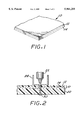
- FIG. 1 illustrates an improved entry overlay sheet in accordance with this invention.
- FIG. 2 illustrates the drilling of a hole in a printed circuit board employing the improved entry overlay sheet in accordance with the invention.
- FIG. 3 shows an alternate embodiment of an improved entry overlay sheet in accordance with the invention.
- FIG. 4 illustrates the drilling of a hole in a printed circuit board using the entry overlay sheet of FIG. 3.
- FIG. 1 illustrates an exemplary embodiment of an improved entry overlay sheet 10 in accordance with the invention.
- the sheet 10 comprises a thin layer 12 of homogeneous polymer material selected from the thermoset or thermoplastic families of resins which can be fabricated in sheet form.
- the layer 12 is in turn applied to a relatively hard layer 14, e.g. a layer of non-metallic material such as a phenolic or melamine (thermoset resins), to create an entry overlay sheet which is stiffer than that described in U.S. Pat. No. 5,067,859.
- Melamine is a chemical name for an amino resin made from urea and ammonia. Phenolic and melamine resins are both thermoset resins which do not melt at elevated temperatures, but rather will turn to powder.
- the melamine resin is available commercially, e.g. from American Standard.
- the layer 14 could be alternatively fabricated of a metal material, such as aluminum or copper foil.
- the improved overlay sheet 10 can be used advantageously both in micro-hole drilling and drilling with larger drill sizes.
- the layer 12 provides a soft entry for the drill tool, and immobilizes, in a lateral direction sense, the tip of the drill prior to entering the harder layer 14, i.e. the layer 12 prevents the tip of the drill from deflecting along directions transverse to the drill axis.
- the layer 12 has a preferred thickness in the range of 3 to 8 thousandths (0.003 to 0.008) of an inch.
- the hard layer 14 has a preferred thickness in the range of 3 to 12 thousandths of an inch.
- exemplary embodiments of the overlay sheet 10 will have a preferred composite thickness in the range of 6 to 20 thousandths (0.006 to 0.020) of an inch.
- the preferred embodiment employs a phenolic or melamine layer 14, and may be fabricated in the following manner.
- Phenolic or melamine is typically made by passing a sheet/web of paper through a liquid phenolic or melamine bath, with the excess resin material removed by rollers or squeegees. The resulting paper is impregnated with the phenolic or melamine resin, and is dried in an oven. This leaves the paper web with resin in a somewhat flexible, non-cured state, i.e. the resin has not yet polymerized.
- the paper is then cut into sheets which are stacked between separator plates to form a lamination. This lamination is then placed in a heated press to cure at an elevated temperature.
- the curing step results in a final, phenolic or melamine product.
- the soft layer 12 can be bonded to the phenolic or melamine sheet during the second curing step.
- a preferred material for the layer 12 is nylon, which is stable to 500 degrees F.
- the soft nylon layer is placed on each uncured phenolic sheet prior to the hot press step. During the hot press step, the nylon becomes adhered to a surface of the phenolic/melamine as the latter sheet is curing. This will result in the sheet 10.
- the nylon layer may be coated with a primer to enhance adhesion.
- the layer 14 is a metal foil layer.
- the polymer layer 12 can be affixed to the hard metal foil layer 14 with an adhesive.
- adhesives There are many types of adhesives which can be used for this purpose. The selection is guided by the mechanical and thermal properties of the adhesive, as it is important that the adhesive will not melt during the drilling process and adhere to the drill bit.
- the layer 12 can be laminated to the foil layer 14 with heat, or the layer 12 can be extruded and bonded to the layer 14 in one operation. Most films are calendared, wherein a steel drum is coated with a molten polymer material. The metal foil can be placed on the drum, pretreated to assure bonding of the foil and molten polymer, and coated with the molten material.
- Thin sheets of the polymer layer 12 can be made through casting, extruding, calendaring or pressing methods currently used to fabricate polymer films.
- thermoplastic materials believed suitable for fabricating the layer 12 include nylon, cellulose triacetate, polyester, polyimid, polyetherimid, and polycarbonate.
- a thermoset material which may be used to fabricate the layer 12 is FR-4 resin formed into a thin sheet.
- the surface finish of the layer 12 can be either mat or smooth, free of pits, voids or dents.
- the material comprising the layer 12 is ideally free of pin holes. The cost of the material is an important factor, to minimize the cost of the entry overlay sheet.
- a plastic sheet to be used as layer 12 can be formed from a liquid bath of resin.
- an extrusion of the melted material through calendaring machines is a preferred technique for making the film. Calendaring is accomplished by passing the molten material through opposing rollers until a desired thickness is formed.
- FIG. 2 illustrates a method of drilling a printed circuit board 20 employing the entry overlay sheet 10 in accordance with the invention.
- the drill bit 30 is carried by a drilling spindle 22, which typically includes a pressure foot 24.
- a drilling spindle 22 typically includes a pressure foot 24.
- the spindle 22 and pressure foot 24 are lowered, the pressure foot 24 contacting the exposed surface of the layer 12 and securing it, and the rotating drill bit 30 is lowered or advanced into the material to be drilled.
- the layer 12, layer 14 and then the printed circuit board 20 are drilled in succession.
- FIG. 3 illustrates an alternate embodiment of an entry overlay sheet 10' in accordance with the invention.
- the sheet 10 of FIG. 1 has an "up" side and a “down” side relative to the printed circuit board, in that the layer 12 is positioned to first receive the drill tool.
- the sheet 10' is "reversible” in the sense that either side can be positioned against the printed circuit board. This is accomplished by providing the sheet 10' with layers 12A and 12B which sandwich layer 14.
- the layers 12A and 12B are identical to layer 12 (FIG. 1), and thus are each thin layers of a homogeneous polymer material selected from the thermoset or thermoplastic families of resins which can be fabricated in sheet form.
- the layer 14 is a relatively hard layer as in layer 14 of FIG. 1, e.g. a layer of non-metallic material such as a phenolic or melamine (thermoset resins), or a metal foil layer.
- the layers 12A, 14 and 12B are bonded together.
- the sheet 10' can be fabricated by techniques similar to those described above for fabrication of the sheet 10.
- the sheet 10' is somewhat more expensive to fabricate, since two polymer layers 12A, 12B are employed, but provides the advantage that either side of the sheet can be laid against the printed circuit board prior to drilling operations.
- FIG. 4 illustrates a method of drilling a printed circuit board 20 employing the entry overlay sheet 10' in accordance with the invention.
- the drill bit 30 is carried by a drilling spindle 22, which typically includes a pressure foot 24.
- a drilling spindle 22 typically includes a pressure foot 24.
- the spindle 22 and pressure foot 24 are lowered, the pressure foot 24 contacting the exposed surface of the layer 12A and securing it, and the rotating drill bit 30 is lowered or advanced into the material to be drilled.
- the layer 12A, layer 14, layer 12B and then the printed circuit board 20 are drilled in succession.
Landscapes
- Engineering & Computer Science (AREA)
- Manufacturing & Machinery (AREA)
- Microelectronics & Electronic Packaging (AREA)
- Mechanical Engineering (AREA)
- Perforating, Stamping-Out Or Severing By Means Other Than Cutting (AREA)
- Laminated Bodies (AREA)
Abstract
An overlay sheet having a first thin layer of a polymer material, a second thin layer of a hard material such as a phenolic, melamine or metal foil, and a third thin layer of a polymer material, the first and third layers sandwiching the second layer. The sheet is applied to a surface of a printed circuit board such that the third layer is against the board surface, and the first layer is exposed to receive the drill bit. During drilling operations, the drill bit is advanced initially through the softer first layer of the polymer material, immobilizing the tip of the drill bit against lateral movement, then through the harder layer, then through the softer third layer, and finally through the printed circuit board. The harder layer prevents formation of burrs, and the polymer material inhibits drill bit wander.
Description
This application is a continuation-in-part of application Ser. No. 08/688,362, filed Jul. 30, 1996 now U.S. Pat. No. 5,785,465.
This invention relates to the fabrication of printed circuit boards, and more particularly to an improved entry overlay sheet and method for drilling micro-holes and larger holes.
Applicant's U.S. Pat. No. 5,067,859, the entire contents of which are incorporated herein by this reference, describes a method for drilling small holes in printed circuit boards. This invention is an improvement over the invention described in this issued patent. The '859 patent describes the use of an entry overlay sheet which is a homogeneous layer comprising a polymer material having a thickness of about ten thousandths of an inch or smaller. While this sheet works very well in the drilling of micro-sized holes, on the order of 0.003 to 0.005 inches in diameter, the ability to drill larger holes, say on the order of 0.005 to 0.015 inches, is impaired, due to the flexibility of the thin overlay sheet. The layer of polymer material will help to minimize the drill wander, but does not prevent formation of burrs in holes drilled with larger drill sizes. The polymer film overlay material, with its inherent softness and lack of rigidity, tends to lift off the surface of the drilled laminate with the return stroke of the drill. Such lift-off may cause collecting of debris under the drill entry overlay sheet.
It is therefore an object of this invention to provide an improved entry overlay sheet and method for drilling holes in a printed circuit board which is suitable for drilling of micro- and larger holes.
A method is described for drilling a printed circuit board, comprising the steps of:
placing an entry overlay sheet on a surface of the printed circuit board, wherein the entry overlay sheet comprises a first thin layer comprising a polymer material having a thickness of about ten thousandths of an inch or smaller, a second thin layer of a hard material, and a third thin layer comprising a polymer material having a thickness of about ten thousandths of an inch or smaller, with the first layer and the third layer sandwiching therebetween the second layer; and
drilling through the first thin layer, the second thin layer, the third thin layer and the printed circuit board in succession with a drilling tool.
In accordance with another aspect of the invention, an entry overlay sheet is described for facilitating drilling of holes in printed circuit boards. The entry overlay sheet includes a first thin layer of a polymer material having a thickness of about ten thousandths of an inch or smaller, a second thin layer of a hard material having a thickness of about twelve thousandths of an inch or smaller, and a third thin layer of a polymer material having a thickness of about ten thousandths of an inch or smaller. The first thin layer and third thin layer sandwich the second layer, the third layer for application against the surface of the printed circuit board.
These and other features and advantages of the present invention will become more apparent from the following detailed description of an exemplary embodiment thereof, as illustrated in the accompanying drawings, in which:
FIG. 1 illustrates an improved entry overlay sheet in accordance with this invention.
FIG. 2 illustrates the drilling of a hole in a printed circuit board employing the improved entry overlay sheet in accordance with the invention.
FIG. 3 shows an alternate embodiment of an improved entry overlay sheet in accordance with the invention.
FIG. 4 illustrates the drilling of a hole in a printed circuit board using the entry overlay sheet of FIG. 3.
FIG. 1 illustrates an exemplary embodiment of an improved entry overlay sheet 10 in accordance with the invention. The sheet 10 comprises a thin layer 12 of homogeneous polymer material selected from the thermoset or thermoplastic families of resins which can be fabricated in sheet form. The layer 12 is in turn applied to a relatively hard layer 14, e.g. a layer of non-metallic material such as a phenolic or melamine (thermoset resins), to create an entry overlay sheet which is stiffer than that described in U.S. Pat. No. 5,067,859. Melamine is a chemical name for an amino resin made from urea and ammonia. Phenolic and melamine resins are both thermoset resins which do not melt at elevated temperatures, but rather will turn to powder. The melamine resin is available commercially, e.g. from American Standard. The layer 14 could be alternatively fabricated of a metal material, such as aluminum or copper foil.
The improved overlay sheet 10 can be used advantageously both in micro-hole drilling and drilling with larger drill sizes. The layer 12 provides a soft entry for the drill tool, and immobilizes, in a lateral direction sense, the tip of the drill prior to entering the harder layer 14, i.e. the layer 12 prevents the tip of the drill from deflecting along directions transverse to the drill axis.
The layer 12 has a preferred thickness in the range of 3 to 8 thousandths (0.003 to 0.008) of an inch. The hard layer 14 has a preferred thickness in the range of 3 to 12 thousandths of an inch. Thus, exemplary embodiments of the overlay sheet 10 will have a preferred composite thickness in the range of 6 to 20 thousandths (0.006 to 0.020) of an inch.
The preferred embodiment employs a phenolic or melamine layer 14, and may be fabricated in the following manner. Phenolic or melamine is typically made by passing a sheet/web of paper through a liquid phenolic or melamine bath, with the excess resin material removed by rollers or squeegees. The resulting paper is impregnated with the phenolic or melamine resin, and is dried in an oven. This leaves the paper web with resin in a somewhat flexible, non-cured state, i.e. the resin has not yet polymerized. The paper is then cut into sheets which are stacked between separator plates to form a lamination. This lamination is then placed in a heated press to cure at an elevated temperature. After a subsequent cooling stage, the curing step results in a final, phenolic or melamine product. To fabricate the entry overlay sheet embodying this invention, the soft layer 12 can be bonded to the phenolic or melamine sheet during the second curing step. A preferred material for the layer 12 is nylon, which is stable to 500 degrees F. The soft nylon layer is placed on each uncured phenolic sheet prior to the hot press step. During the hot press step, the nylon becomes adhered to a surface of the phenolic/melamine as the latter sheet is curing. This will result in the sheet 10. The nylon layer may be coated with a primer to enhance adhesion.
In an alternate embodiment, the layer 14 is a metal foil layer. The polymer layer 12 can be affixed to the hard metal foil layer 14 with an adhesive. There are many types of adhesives which can be used for this purpose. The selection is guided by the mechanical and thermal properties of the adhesive, as it is important that the adhesive will not melt during the drilling process and adhere to the drill bit. Alternatively, the layer 12 can be laminated to the foil layer 14 with heat, or the layer 12 can be extruded and bonded to the layer 14 in one operation. Most films are calendared, wherein a steel drum is coated with a molten polymer material. The metal foil can be placed on the drum, pretreated to assure bonding of the foil and molten polymer, and coated with the molten material.
Thin sheets of the polymer layer 12 can be made through casting, extruding, calendaring or pressing methods currently used to fabricate polymer films. Examples of thermoplastic materials believed suitable for fabricating the layer 12 include nylon, cellulose triacetate, polyester, polyimid, polyetherimid, and polycarbonate. One example of a thermoset material which may be used to fabricate the layer 12 is FR-4 resin formed into a thin sheet. The surface finish of the layer 12 can be either mat or smooth, free of pits, voids or dents. The material comprising the layer 12 is ideally free of pin holes. The cost of the material is an important factor, to minimize the cost of the entry overlay sheet.
A plastic sheet to be used as layer 12 can be formed from a liquid bath of resin. To assure homogeneity and flatness of the finished product, an extrusion of the melted material through calendaring machines is a preferred technique for making the film. Calendaring is accomplished by passing the molten material through opposing rollers until a desired thickness is formed.
The fabrication of phenolics, melamines and metal foils such as aluminum foil or copper foil is well known.
FIG. 2 illustrates a method of drilling a printed circuit board 20 employing the entry overlay sheet 10 in accordance with the invention. The drill bit 30 is carried by a drilling spindle 22, which typically includes a pressure foot 24. With the entry overlay sheet 10 placed on top of the printed circuit board 20, with the polymer film 12 exposed, the spindle 22 and pressure foot 24 are lowered, the pressure foot 24 contacting the exposed surface of the layer 12 and securing it, and the rotating drill bit 30 is lowered or advanced into the material to be drilled. The layer 12, layer 14 and then the printed circuit board 20 are drilled in succession.
FIG. 3 illustrates an alternate embodiment of an entry overlay sheet 10' in accordance with the invention. The sheet 10 of FIG. 1 has an "up" side and a "down" side relative to the printed circuit board, in that the layer 12 is positioned to first receive the drill tool. The sheet 10' is "reversible" in the sense that either side can be positioned against the printed circuit board. This is accomplished by providing the sheet 10' with layers 12A and 12B which sandwich layer 14. In an exemplary embodiment, the layers 12A and 12B are identical to layer 12 (FIG. 1), and thus are each thin layers of a homogeneous polymer material selected from the thermoset or thermoplastic families of resins which can be fabricated in sheet form. The layer 14 is a relatively hard layer as in layer 14 of FIG. 1, e.g. a layer of non-metallic material such as a phenolic or melamine (thermoset resins), or a metal foil layer.
The layers 12A, 14 and 12B are bonded together. The sheet 10' can be fabricated by techniques similar to those described above for fabrication of the sheet 10. The sheet 10' is somewhat more expensive to fabricate, since two polymer layers 12A, 12B are employed, but provides the advantage that either side of the sheet can be laid against the printed circuit board prior to drilling operations.
FIG. 4 illustrates a method of drilling a printed circuit board 20 employing the entry overlay sheet 10' in accordance with the invention. The drill bit 30 is carried by a drilling spindle 22, which typically includes a pressure foot 24. With the entry overlay sheet 10' placed on top of the printed circuit board 20, with the polymer layer 12A exposed and the polymer layer 12B disposed against the surface of the board 20, the spindle 22 and pressure foot 24 are lowered, the pressure foot 24 contacting the exposed surface of the layer 12A and securing it, and the rotating drill bit 30 is lowered or advanced into the material to be drilled. The layer 12A, layer 14, layer 12B and then the printed circuit board 20 are drilled in succession.
It is understood that the above-described embodiments are merely illustrative of the possible specific embodiments which may represent principles of the present invention. Other arrangements may readily be devised in accordance with these principles by those skilled in the art without departing from the scope and spirit of the invention.
Claims (26)
1. A method for drilling a printed circuit board, comprising the steps of:
placing an entry overlay sheet on a surface of the printed circuit board, wherein the entry overlay sheet comprises a first thin layer comprising a polymer material having a thickness of about ten thousandths of an inch or smaller, a second thin layer of a hard material, and a third thin layer comprising a polymer material having a thickness of about ten thousandths of an inch or smaller, with the first layer and the third layer sandwiching therebetween the second layer; and
drilling through the first thin layer, the second thin layer, the third thin layer and the printed circuit board in succession with a drilling tool.
2. The method of claim 1 wherein the first layer has a thickness in the range of three to eight thousandths of an inch.
3. The method of claim 1 wherein the second layer has a thickness in the range of three to twelve thousandths of an inch.
4. The method of claim 1 wherein the third layer has a thickness in the range of three to eight thousandths of an inch.
5. The method of claim 1 wherein the second layer is fabricated from a metal material.
6. The method of claim 1 wherein the second layer is a fabricated from aluminum or copper.
7. The method of claim 1 wherein the second layer is fabricated from a phenolic material.
8. The method of claim 1 wherein the second layer is fabricated from a melamine material.
9. The method of claim 1 wherein the first layer has a thickness in the range of three to eight thousandths of an inch, the second layer has a thickness in the range of three to twelve thousandths of an inch, the third layer has a thickness in the range of three to eight thousandths of an inch, and the entry overly sheet has a composite thickness in the range of nine to twenty-eight thousandths of an inch.
10. The method of claim 1 wherein the first layer is a homogeneous layer of a polymer material substantially free of inclusion of any foreign material.
11. The method of claim 1 wherein the polymer material of the first layer and the third layer is selected from the materials group consisting of nylon, polyester, cellulose triacetate, polyetherimid, polyphenylene oxide or polycarbonate.
12. The method of claim 1 wherein the polymer material is selected from the family of thermoset resins.
13. The method of claim 1 wherein the polymer material is selected from the family of thermoplastic materials.
14. An entry overlay sheet for facilitating drilling of holes in printed circuit boards, comprising:
a first thin layer of a polymer material having a thickness of about ten thousandths of an inch or smaller;
a second thin layer of a hard material having a thickness of about twelve thousandths of an inch or smaller;
a third thin layer of a polymer material having a thickness of about ten thousandths of an inch or smaller;
the first thin layer and third thin layer sandwiching therebetween the second layer, the third layer for application against the surface of the printed circuit board.
15. The sheet of claim 14 wherein the first layer has a thickness in the range of three to eight thousandths of an inch.
16. The sheet of claim 14 wherein the second layer has a thickness in the range of three to twelve thousandths of an inch.
17. The sheet of claim 14 wherein the third layer has a thickness in the range of three to eight thousandths of an inch.
18. The sheet of claim 14 wherein the second layer is fabricated from a metal material.
19. The sheet of claim 18 wherein the second layer is a fabricated from aluminum or copper.
20. The sheet of claim 14 wherein the second layer is fabricated from a phenolic material.
21. The sheet of claim 14 wherein the second layer is fabricated from a melamine material.
22. The sheet of claim 14 wherein the first layer has a thickness in the range of three to eight thousandths of an inch, the second layer has a thickness in the range of three to twelve thousandths of an inch, the third layer has a thickness in the range of three to eight thousandths of an inch, and the entry overly sheet has a composite thickness in the range of nine to twenty-eight thousandths of an inch.
23. The sheet of claim 14 wherein the first layer and the third layer are each a homogeneous layer of a polymer material substantially free of inclusion of any foreign material.
24. The sheet of claim 14 wherein the polymer material of the first layer is selected from the materials group consisting of nylon, polyester, cellulose triacetate, polyetherimid, polyphenylene oxide or polycarbonate.
25. The sheet of claim 14 wherein the polymer material is selected from the family of thermoset resins.
26. The sheet of claim 14 wherein the polymer material is selected from the family of thermoplastic materials.
Priority Applications (1)
| Application Number | Priority Date | Filing Date | Title |
|---|---|---|---|
| US09/121,978 US5961255A (en) | 1996-07-30 | 1998-07-24 | Entry overlay sheet and method for drilling holes |
Applications Claiming Priority (2)
| Application Number | Priority Date | Filing Date | Title |
|---|---|---|---|
| US08/688,362 US5785465A (en) | 1996-07-30 | 1996-07-30 | Entry overlay sheet and method for drilling holes |
| US09/121,978 US5961255A (en) | 1996-07-30 | 1998-07-24 | Entry overlay sheet and method for drilling holes |
Related Parent Applications (1)
| Application Number | Title | Priority Date | Filing Date |
|---|---|---|---|
| US08/688,362 Continuation-In-Part US5785465A (en) | 1996-07-30 | 1996-07-30 | Entry overlay sheet and method for drilling holes |
Publications (1)
| Publication Number | Publication Date |
|---|---|
| US5961255A true US5961255A (en) | 1999-10-05 |
Family
ID=46254144
Family Applications (1)
| Application Number | Title | Priority Date | Filing Date |
|---|---|---|---|
| US09/121,978 Expired - Fee Related US5961255A (en) | 1996-07-30 | 1998-07-24 | Entry overlay sheet and method for drilling holes |
Country Status (1)
| Country | Link |
|---|---|
| US (1) | US5961255A (en) |
Cited By (22)
| Publication number | Priority date | Publication date | Assignee | Title |
|---|---|---|---|---|
| DE10056184A1 (en) * | 2000-11-13 | 2002-05-29 | Cimatec Gmbh Produkte Fuer Lei | drilling |
| US6565295B2 (en) * | 2000-06-05 | 2003-05-20 | Risho Kogyo Co., Ltd. | Entry board for drilling |
| US20030100456A1 (en) * | 2001-10-31 | 2003-05-29 | Takuya Hasaki | Entry sheet for drilling and method for drilling hole |
| WO2003077619A1 (en) * | 2002-03-06 | 2003-09-18 | Kennametal Inc. | Process for drilling circuit board panels |
| US20040023059A1 (en) * | 2000-09-14 | 2004-02-05 | Shingo Kaburagi | Entry boards for use in drilling small holes |
| US20040086741A1 (en) * | 2001-02-16 | 2004-05-06 | Japp Robert M. | Drill stack formation |
| KR100452278B1 (en) * | 2002-03-20 | 2004-10-12 | 김병식 | Backup board for punching holes of printed circuit board |
| US20050022381A1 (en) * | 2002-10-28 | 2005-02-03 | Soqi Kabushiki Kaisha | Method of making gear pump |
| SG115399A1 (en) * | 2000-09-04 | 2005-10-28 | Mitsubishi Gas Chemical Co | Lubricant sheet for making hole and method of making hole with drill |
| US20060216486A1 (en) * | 2005-03-28 | 2006-09-28 | Te-Han Wang | Entry board suitable for use during drilling of an integrated circuit board |
| KR100728765B1 (en) * | 2007-02-02 | 2007-06-19 | 삼성전기주식회사 | Method for manufacturing substrate using entry board for drill processing and substrate manufactured thereby |
| KR100728749B1 (en) | 2005-12-14 | 2007-06-19 | 삼성전기주식회사 | Entry board for drill processing and method for manufacturing thereof |
| US8323798B2 (en) | 2007-09-28 | 2012-12-04 | Tri-Star Laminates, Inc. | Systems and methods for drilling holes in printed circuit boards |
| CN106142205A (en) * | 2015-04-22 | 2016-11-23 | 大连崇达电路有限公司 | Diameter 0.25mm following printed wiring board finished hole processing method |
| CN106180784A (en) * | 2016-07-01 | 2016-12-07 | 中航飞机股份有限公司西安飞机分公司 | The control method of lower wall panels drilling burr on a kind of aircraft |
| JP2017006996A (en) * | 2015-06-17 | 2017-01-12 | 三菱瓦斯化学株式会社 | Metal cutting method |
| CN106573395A (en) * | 2014-08-26 | 2017-04-19 | 3M创新有限公司 | Damped abrasive cutter |
| CN106793489A (en) * | 2016-12-20 | 2017-05-31 | 高德(江苏)电子科技有限公司 | A kind of process for improving Rigid Flex aperture peak |
| JP6212193B1 (en) * | 2016-08-30 | 2017-10-11 | 台虹科技股▲分▼有限公司 | Coating films used in circuit board punching processes. |
| CN109094151A (en) * | 2018-07-05 | 2018-12-28 | 苏州广型模具有限公司 | Carbide cutting cover board |
| US20190184472A1 (en) * | 2016-06-13 | 2019-06-20 | Mitsubishi Gas Chemical Company, Inc. | Drill Bit And Hole Formation Method |
| US11931866B2 (en) | 2018-10-19 | 2024-03-19 | Saint-Gobain Abrasives, Inc. | Grinding wheel assembly |
Citations (12)
| Publication number | Priority date | Publication date | Assignee | Title |
|---|---|---|---|---|
| US3700341A (en) * | 1970-07-27 | 1972-10-24 | Lcoa Laminating Co Of America | Laminated board and method of making same |
| US4019826A (en) * | 1973-06-18 | 1977-04-26 | Lcoa Laminating Company Of America | Method for drilling circuit boards |
| US4269549A (en) * | 1979-07-30 | 1981-05-26 | Lcoa Laminating Company Of America | Method for drilling circuit boards |
| US4311419A (en) * | 1979-07-30 | 1982-01-19 | Lcoa Laminating Company Of America | Method for drilling circuit boards |
| US4605344A (en) * | 1983-09-20 | 1986-08-12 | Siemens Aktiengesellschaft | Device for drilling holes in a stack of plates |
| US4781495A (en) * | 1986-10-14 | 1988-11-01 | Lubra Sheet Corp. | Dry lubricant drilling of thru-holes in printed circuit boards |
| US5067859A (en) * | 1990-02-15 | 1991-11-26 | Systems Division Incorporated | Method for drilling small holes in printed circuit boards |
| US5082402A (en) * | 1990-08-08 | 1992-01-21 | Mitsubishi Gas Chemical Co. Ltd. | Method of drilling of through-holes in printed circuit board panels |
| US5480269A (en) * | 1993-06-07 | 1996-01-02 | Mitsubishi Gas Chemical Company, Inc. | Method of drilling a hole for printed wiring board |
| US5507603A (en) * | 1993-08-05 | 1996-04-16 | Dai-Ichi Kogyo Seiyaku Co., Ltd. | Method for drilling thru-holes on a lamination substrate and a sheet used therein |
| US5716168A (en) * | 1994-10-27 | 1998-02-10 | Janoff; Marshall A. | Method of drilling holes in printed circuit boards with backup board material |
| US5785465A (en) * | 1996-07-30 | 1998-07-28 | Systems Division Incorporated | Entry overlay sheet and method for drilling holes |
-
1998
- 1998-07-24 US US09/121,978 patent/US5961255A/en not_active Expired - Fee Related
Patent Citations (12)
| Publication number | Priority date | Publication date | Assignee | Title |
|---|---|---|---|---|
| US3700341A (en) * | 1970-07-27 | 1972-10-24 | Lcoa Laminating Co Of America | Laminated board and method of making same |
| US4019826A (en) * | 1973-06-18 | 1977-04-26 | Lcoa Laminating Company Of America | Method for drilling circuit boards |
| US4269549A (en) * | 1979-07-30 | 1981-05-26 | Lcoa Laminating Company Of America | Method for drilling circuit boards |
| US4311419A (en) * | 1979-07-30 | 1982-01-19 | Lcoa Laminating Company Of America | Method for drilling circuit boards |
| US4605344A (en) * | 1983-09-20 | 1986-08-12 | Siemens Aktiengesellschaft | Device for drilling holes in a stack of plates |
| US4781495A (en) * | 1986-10-14 | 1988-11-01 | Lubra Sheet Corp. | Dry lubricant drilling of thru-holes in printed circuit boards |
| US5067859A (en) * | 1990-02-15 | 1991-11-26 | Systems Division Incorporated | Method for drilling small holes in printed circuit boards |
| US5082402A (en) * | 1990-08-08 | 1992-01-21 | Mitsubishi Gas Chemical Co. Ltd. | Method of drilling of through-holes in printed circuit board panels |
| US5480269A (en) * | 1993-06-07 | 1996-01-02 | Mitsubishi Gas Chemical Company, Inc. | Method of drilling a hole for printed wiring board |
| US5507603A (en) * | 1993-08-05 | 1996-04-16 | Dai-Ichi Kogyo Seiyaku Co., Ltd. | Method for drilling thru-holes on a lamination substrate and a sheet used therein |
| US5716168A (en) * | 1994-10-27 | 1998-02-10 | Janoff; Marshall A. | Method of drilling holes in printed circuit boards with backup board material |
| US5785465A (en) * | 1996-07-30 | 1998-07-28 | Systems Division Incorporated | Entry overlay sheet and method for drilling holes |
Cited By (32)
| Publication number | Priority date | Publication date | Assignee | Title |
|---|---|---|---|---|
| US6565295B2 (en) * | 2000-06-05 | 2003-05-20 | Risho Kogyo Co., Ltd. | Entry board for drilling |
| KR100814048B1 (en) * | 2000-06-05 | 2008-03-18 | 리쇼 고교 가부시키가이샤 | Entry board for drilling |
| SG115399A1 (en) * | 2000-09-04 | 2005-10-28 | Mitsubishi Gas Chemical Co | Lubricant sheet for making hole and method of making hole with drill |
| US20040023059A1 (en) * | 2000-09-14 | 2004-02-05 | Shingo Kaburagi | Entry boards for use in drilling small holes |
| US6890664B2 (en) * | 2000-09-14 | 2005-05-10 | Ohtomo Chemical Inc., Corp. | Entry boards for use in drilling small holes |
| DE10056184A1 (en) * | 2000-11-13 | 2002-05-29 | Cimatec Gmbh Produkte Fuer Lei | drilling |
| US7329446B2 (en) * | 2001-02-16 | 2008-02-12 | International Business Machines Corporation | Drill stack formation |
| US20040086741A1 (en) * | 2001-02-16 | 2004-05-06 | Japp Robert M. | Drill stack formation |
| US6866450B2 (en) * | 2001-10-31 | 2005-03-15 | Mitsubishi Gas Chemical Company, Inc. | Entry sheet for drilling and method for drilling hole |
| US20030100456A1 (en) * | 2001-10-31 | 2003-05-29 | Takuya Hasaki | Entry sheet for drilling and method for drilling hole |
| WO2003077619A1 (en) * | 2002-03-06 | 2003-09-18 | Kennametal Inc. | Process for drilling circuit board panels |
| KR100452278B1 (en) * | 2002-03-20 | 2004-10-12 | 김병식 | Backup board for punching holes of printed circuit board |
| US20050022381A1 (en) * | 2002-10-28 | 2005-02-03 | Soqi Kabushiki Kaisha | Method of making gear pump |
| US6996905B2 (en) * | 2002-10-28 | 2006-02-14 | Soqi Kabushiki Kaisha | Method of making gear pump |
| US20060216486A1 (en) * | 2005-03-28 | 2006-09-28 | Te-Han Wang | Entry board suitable for use during drilling of an integrated circuit board |
| KR100728749B1 (en) | 2005-12-14 | 2007-06-19 | 삼성전기주식회사 | Entry board for drill processing and method for manufacturing thereof |
| KR100728765B1 (en) * | 2007-02-02 | 2007-06-19 | 삼성전기주식회사 | Method for manufacturing substrate using entry board for drill processing and substrate manufactured thereby |
| US8323798B2 (en) | 2007-09-28 | 2012-12-04 | Tri-Star Laminates, Inc. | Systems and methods for drilling holes in printed circuit boards |
| US8802237B2 (en) | 2007-09-28 | 2014-08-12 | Tri-Star Laminates, Inc. | Entry sheet for drilling holes in printed circuit boards |
| US20170239841A1 (en) * | 2014-08-26 | 2017-08-24 | 3M Innovative Properties Company | Damped abrasive cutter |
| CN106573395A (en) * | 2014-08-26 | 2017-04-19 | 3M创新有限公司 | Damped abrasive cutter |
| CN106573395B (en) * | 2014-08-26 | 2021-02-05 | 3M创新有限公司 | Damping abrasive cutter |
| CN106142205A (en) * | 2015-04-22 | 2016-11-23 | 大连崇达电路有限公司 | Diameter 0.25mm following printed wiring board finished hole processing method |
| JP2017006996A (en) * | 2015-06-17 | 2017-01-12 | 三菱瓦斯化学株式会社 | Metal cutting method |
| US20190184472A1 (en) * | 2016-06-13 | 2019-06-20 | Mitsubishi Gas Chemical Company, Inc. | Drill Bit And Hole Formation Method |
| CN106180784A (en) * | 2016-07-01 | 2016-12-07 | 中航飞机股份有限公司西安飞机分公司 | The control method of lower wall panels drilling burr on a kind of aircraft |
| JP6212193B1 (en) * | 2016-08-30 | 2017-10-11 | 台虹科技股▲分▼有限公司 | Coating films used in circuit board punching processes. |
| JP2018037627A (en) * | 2016-08-30 | 2018-03-08 | 台虹科技股▲分▼有限公司 | Coating film used for punching process of circuit board |
| CN106793489A (en) * | 2016-12-20 | 2017-05-31 | 高德(江苏)电子科技有限公司 | A kind of process for improving Rigid Flex aperture peak |
| CN106793489B (en) * | 2016-12-20 | 2019-04-02 | 高德(江苏)电子科技有限公司 | A kind of process improving Rigid Flex aperture peak |
| CN109094151A (en) * | 2018-07-05 | 2018-12-28 | 苏州广型模具有限公司 | Carbide cutting cover board |
| US11931866B2 (en) | 2018-10-19 | 2024-03-19 | Saint-Gobain Abrasives, Inc. | Grinding wheel assembly |
Similar Documents
| Publication | Publication Date | Title |
|---|---|---|
| US5961255A (en) | Entry overlay sheet and method for drilling holes | |
| US5785465A (en) | Entry overlay sheet and method for drilling holes | |
| JP3142554B2 (en) | Multilayer films and laminates for printed circuit board manufacture | |
| FI111510B (en) | A printed circuit board component and a method of manufacturing the component | |
| US5435671A (en) | Drilling printed circuit boards and entry and backing boards therefor | |
| EP0411142B1 (en) | Outer layer material of multilayer printed wiring board and production thereof | |
| US4269549A (en) | Method for drilling circuit boards | |
| KR20000047687A (en) | Method of vacuum-laminating adhesive film | |
| CA2349246A1 (en) | Method for producing a multilayer coextrudate and a coextrudate produced according thereto | |
| WO1981000367A1 (en) | Entry material and method for drilling circuit boards | |
| JP2790708B2 (en) | Process for protecting protected conductive oil and electrodeposited metal oil during processing | |
| US5460680A (en) | Method for manufacturing multi-layer printed board | |
| CA2273542A1 (en) | Thin film laminates | |
| US4690845A (en) | Method and apparatus for laminating flexible printed circuits | |
| JPH062369B2 (en) | Surface roughening film and sheet made of poly-4-methyl-1-pentene for manufacturing multilayer printed wiring board | |
| KR100369699B1 (en) | Technique for partially joining foils and separator sheets | |
| GB2252522A (en) | Drilling printed circuit boards and entry boards therefor | |
| GB2233601A (en) | Method of manufacturing resin overlay plate | |
| US4857400A (en) | Stratiform press pads and methods for use thereof in laminating flexible printed circuits | |
| EP0528963A1 (en) | Process for the production of a multilayer printed circuit board. | |
| JP2001205763A (en) | Protective film for prepreg | |
| JP2000151116A (en) | Method and device for manufacturing multilayer printed board | |
| JP4759896B2 (en) | Manufacturing method of printed wiring board manufacturing material | |
| WO1985003669A1 (en) | Method and apparatus for laminating flexible printed circuits | |
| JPS5875884A (en) | Method of producing printed circuit board |
Legal Events
| Date | Code | Title | Description |
|---|---|---|---|
| AS | Assignment |
Owner name: SYSTEMS DIVISION INCORPORATED, CALIFORNIA Free format text: ASSIGNMENT OF ASSIGNORS INTEREST;ASSIGNOR:KORBONSKI, JOHN A.;REEL/FRAME:009551/0978 Effective date: 19981013 |
|
| REMI | Maintenance fee reminder mailed | ||
| LAPS | Lapse for failure to pay maintenance fees | ||
| STCH | Information on status: patent discontinuation |
Free format text: PATENT EXPIRED DUE TO NONPAYMENT OF MAINTENANCE FEES UNDER 37 CFR 1.362 |
|
| FP | Expired due to failure to pay maintenance fee |
Effective date: 20031005 |