US5868852A - Partial clean fluorine thermal cleaning process - Google Patents
Partial clean fluorine thermal cleaning process Download PDFInfo
- Publication number
- US5868852A US5868852A US08/801,330 US80133097A US5868852A US 5868852 A US5868852 A US 5868852A US 80133097 A US80133097 A US 80133097A US 5868852 A US5868852 A US 5868852A
- Authority
- US
- United States
- Prior art keywords
- fluorine
- cleaning
- clean
- source
- equipment
- Prior art date
- Legal status (The legal status is an assumption and is not a legal conclusion. Google has not performed a legal analysis and makes no representation as to the accuracy of the status listed.)
- Expired - Fee Related
Links
Images


Classifications
-
- C—CHEMISTRY; METALLURGY
- C23—COATING METALLIC MATERIAL; COATING MATERIAL WITH METALLIC MATERIAL; CHEMICAL SURFACE TREATMENT; DIFFUSION TREATMENT OF METALLIC MATERIAL; COATING BY VACUUM EVAPORATION, BY SPUTTERING, BY ION IMPLANTATION OR BY CHEMICAL VAPOUR DEPOSITION, IN GENERAL; INHIBITING CORROSION OF METALLIC MATERIAL OR INCRUSTATION IN GENERAL
- C23C—COATING METALLIC MATERIAL; COATING MATERIAL WITH METALLIC MATERIAL; SURFACE TREATMENT OF METALLIC MATERIAL BY DIFFUSION INTO THE SURFACE, BY CHEMICAL CONVERSION OR SUBSTITUTION; COATING BY VACUUM EVAPORATION, BY SPUTTERING, BY ION IMPLANTATION OR BY CHEMICAL VAPOUR DEPOSITION, IN GENERAL
- C23C16/00—Chemical coating by decomposition of gaseous compounds, without leaving reaction products of surface material in the coating, i.e. chemical vapour deposition [CVD] processes
- C23C16/44—Chemical coating by decomposition of gaseous compounds, without leaving reaction products of surface material in the coating, i.e. chemical vapour deposition [CVD] processes characterised by the method of coating
- C23C16/52—Controlling or regulating the coating process
-
- C—CHEMISTRY; METALLURGY
- C23—COATING METALLIC MATERIAL; COATING MATERIAL WITH METALLIC MATERIAL; CHEMICAL SURFACE TREATMENT; DIFFUSION TREATMENT OF METALLIC MATERIAL; COATING BY VACUUM EVAPORATION, BY SPUTTERING, BY ION IMPLANTATION OR BY CHEMICAL VAPOUR DEPOSITION, IN GENERAL; INHIBITING CORROSION OF METALLIC MATERIAL OR INCRUSTATION IN GENERAL
- C23C—COATING METALLIC MATERIAL; COATING MATERIAL WITH METALLIC MATERIAL; SURFACE TREATMENT OF METALLIC MATERIAL BY DIFFUSION INTO THE SURFACE, BY CHEMICAL CONVERSION OR SUBSTITUTION; COATING BY VACUUM EVAPORATION, BY SPUTTERING, BY ION IMPLANTATION OR BY CHEMICAL VAPOUR DEPOSITION, IN GENERAL
- C23C16/00—Chemical coating by decomposition of gaseous compounds, without leaving reaction products of surface material in the coating, i.e. chemical vapour deposition [CVD] processes
- C23C16/44—Chemical coating by decomposition of gaseous compounds, without leaving reaction products of surface material in the coating, i.e. chemical vapour deposition [CVD] processes characterised by the method of coating
- C23C16/4401—Means for minimising impurities, e.g. dust, moisture or residual gas, in the reaction chamber
- C23C16/4405—Cleaning of reactor or parts inside the reactor by using reactive gases
-
- C—CHEMISTRY; METALLURGY
- C23—COATING METALLIC MATERIAL; COATING MATERIAL WITH METALLIC MATERIAL; CHEMICAL SURFACE TREATMENT; DIFFUSION TREATMENT OF METALLIC MATERIAL; COATING BY VACUUM EVAPORATION, BY SPUTTERING, BY ION IMPLANTATION OR BY CHEMICAL VAPOUR DEPOSITION, IN GENERAL; INHIBITING CORROSION OF METALLIC MATERIAL OR INCRUSTATION IN GENERAL
- C23C—COATING METALLIC MATERIAL; COATING MATERIAL WITH METALLIC MATERIAL; SURFACE TREATMENT OF METALLIC MATERIAL BY DIFFUSION INTO THE SURFACE, BY CHEMICAL CONVERSION OR SUBSTITUTION; COATING BY VACUUM EVAPORATION, BY SPUTTERING, BY ION IMPLANTATION OR BY CHEMICAL VAPOUR DEPOSITION, IN GENERAL
- C23C16/00—Chemical coating by decomposition of gaseous compounds, without leaving reaction products of surface material in the coating, i.e. chemical vapour deposition [CVD] processes
- C23C16/44—Chemical coating by decomposition of gaseous compounds, without leaving reaction products of surface material in the coating, i.e. chemical vapour deposition [CVD] processes characterised by the method of coating
- C23C16/4412—Details relating to the exhausts, e.g. pumps, filters, scrubbers, particle traps
Definitions
- the present invention is directed to the field of thermal cleaning with nitrogen trifluoride and similar fluorine sources. More specifically, the present invention is directed to cleaning various silicon-containing semiconductor substances from wafers and chemical vapor deposition equipment, including reaction vessels and hardware, using a dynamic flow of nitrogen trifluoride at elevated temperatures with a unique partial clean process.
- the semiconductor industry has experienced a long-felt need to solve the problem of cleaning chemical vapor deposition furnaces and quartz tubes in the furnaces as well as quartz hardware of various undesired substances, such as silicon nitride, polycrystalline silicon, titanium silicide, tungsten silicide and various other silicides, as well as silicon dioxide, which are typically present as undesired films on furnaces and quartz hardware during their deposition on silicon wafers and chips being processed as electronic materials and integrated circuits.
- various undesired substances such as silicon nitride, polycrystalline silicon, titanium silicide, tungsten silicide and various other silicides, as well as silicon dioxide, which are typically present as undesired films on furnaces and quartz hardware during their deposition on silicon wafers and chips being processed as electronic materials and integrated circuits.
- the normal procedure for cleaning is to remove the parts, such as those made of quartz, metals or other materials from a furnace, such as quartz furnace tubes, and perform a wet chemical cleaning. O-ring seals would typically have to be replaced in such an operation, as well as cleaning of lines, doors and other vacuum components.
- the wet chemical cleaning is very costly and time consuming. When the equipment is shut down to pull the quartz parts, it can require up to 18 hours of time. Also, the system necessitates reverification for its operating integrity before it can be used again.
- the wet chemical cleaning application requires special chemicals, equipment and sinks to perform this cleaning. Another disadvantage is that the quartzware is attacked at accelerated rates which affects its reproducibility and reliability of operation. This is especially true when cleaning quartz racks or wafer holders.
- the plasma cleaning method requires the use of another piece of equipment especially designed to perform a cleaning of quartz tubes in place within the chemical vapor deposition furnace equipment.
- the plasma cleaning method does not clean the other quartz parts which are used in the chemical vapor deposition furnace system. This means these parts will need to be chemically wet cleaned, separate and apart from plasma cleaning methods.
- the plasma cleaning equipment takes up space in the manufacturing area, and may prevent other tubes from being used in the system while it is being utilized. If the quartz parts are replaced with another material like silicon carbide, it will make the plasma system application unreliable.
- U.S. Pat. No. 5,421,957 discloses a nitrogen trifluoride cleaning process for semiconductor process reactors and apparatus by controlling the moisture content during the clean operation to be less than 10 parts per million by volume.
- Inert carrier gases for the nitrogen trifluoride are disclosed such as nitrogen, helium, argon or the like.
- the concentration of the inert was from 95.5% to 80% of the etchant mixture.
- U.S. Reissue Patent No. 30,505 discloses a process for plasma etching of a solid material with a binary mixture comprising essentially oxygen and a halocarbon wherein at least one carbon atom in said molecule is linked to a predominance of fluorine atoms.
- a binary mixture comprising essentially oxygen and a halocarbon wherein at least one carbon atom in said molecule is linked to a predominance of fluorine atoms.
- temperatures recited 25°-300° C.
- Temperatures in excess of 1000° C. are necessary to thermally dissociate halocarbons, making this gas impractical for thermal cleaning of semiconductor process equipment.
- U.S. Pat. No. 4,374,698 describes an etch process for differential etching of silicon nitride from silicon dioxide using the combination of carbon tetrafluoride and a halofluorocarbon.
- the gas etchant may include oxygen or nitrous oxide.
- a plasma is necessary to dissociate the halocarbon into species that will react with the solid material.
- the role of the oxygen source in this patent is to volatilize the carbon products into CO and CO 2 . Without oxygen, this process would coat the process equipment with teflon-like material, defeating the usefulness of the process for cleaning.
- U.S. Pat. No. 4,522,681 discloses a method for etching holes in silicon dioxide wherein a dry plasma etch gas of argon, nitrogen trifluoride and oxygen may be used.
- a dry plasma etch gas of argon, nitrogen trifluoride and oxygen may be used.
- Polymeric photoresist materials such as polymethyl methacrylate, ethyl methacrylate, methyl isopropyl ketone as well as copolymers thereof with methacrylic acid may be used.
- This class of photoresist materials was required, versus standard novel AC photoresists, to successfully practice the invention.
- Plasma is necessary to dissociate the fluorine compound into specie that will etch the substrate.
- the role of the oxygen is to etch the photoresist and not the substrate.
- U.S. Pat. No. 4,568,410 discloses a dry plasma etch process for etching silicon nitride using nitrogen trifluoride and oxygen. Good results for etching silicon nitride were found with relative percentages of the nitrogen trifluoride to oxygen recited at column 5, line 65 to be 10-20 SCCM of NF 3 in comparison to 20-35 SCCM for oxygen. The gases are also disclosed as capable of etching common resists.
- U.S. Pat. No. 4,787,957 is directed to a method for plasma desmear and etchbac of epoxy and polyimide materials from a multilayered or double sided printed circuit board using a plasma gas composition in the range of 20-45% NF 3 , the remainder being O 2 .
- EP Application 0 731 497 A2 discloses a thermal clean with diluted nitrogen trifluoride and means for removing the cleaning by-products.
- the prior art has failed to address a commercially successful process for cleaning semiconductor materials or equipment using a gaseous source to produce volatile cleaning by-products which are readily removed from the materials or equipment after cleaning is accomplished.
- the prior art has not addressed a viable method for thermal cleaning with fluorine sources in which minimal start-up time is required to re-initiate the production process in the cleaned equipment.
- the present invention as set forth below overcomes these drawbacks of the prior art.
- the present invention is a thermal process using a source of fluorine for cleaning equipment surfaces in semiconductor manufacturing equipment used to process semiconductor materials, comprising:
- the elevated temperature of step (b) is in the range of approximately 300° to 1000° C.
- the elevated temperature of step (b) is in the range of approximately 400° to 700° C.
- the flow of the source of fluorine is in the range of approximately 1 to 20 standard liters per minute (“SLM").
- the source of fluorine is selected from the group consisting of nitrogen trifluoride, chlorine trifluoride, fluorine, sulfur hexafluoride, carbon tetrafluoride and mixtures thereof.
- an inert gas selected from the group consisting of nitrogen, argon, helium and mixtures thereof is used with the source of fluorine as an etchant mixture.
- the initial evacuation is at a pressure of no greater than 600 torr
- the flow of the source of fluorine is at a pressure of no greater than 750 torr
- the heating is at a temperature of no greater than 400°-700° C.
- the source of fluorine is nitrogen trifluoride which is present in the range of approximately 1 to 50% by volume of the etchant mixture.
- the undesired substances are selected from the group consisting of silicon nitride, siliconoxynitride, silicon dioxide, polysilicon and mixtures thereof.
- the volatile reaction products are monitored to detect an increase in said source of fluorine and said partial clean is terminated when said increase is detected.
- the volatile reaction products are monitored to detect an increase in silicon tetrafluoride and said partial clean is terminated when said increase is detected.
- the increase of nitrogen trifluoride or silicon tetrafluoride has a magnitude of no greater than 20% by volume.
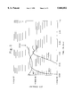
- FIG. 1 is a graph of nitrogen trifluoride, silicon tetrafluoride and nitrogen during a nitrogen trifluoride complete clean not using the process of the present invention.
- the graph is clean time vs. ion content from the clean zone.
- the etch was at a pressure of 500 torr, 550°-600° C., 30% nitrogen trifluoride in nitrogen and a flow of 5.0 standard liters per minute.
- FIG. 2 is a graph of nitrogen trifluoride, silicon tetrafluoride and nitrogen during a nitrogen trifluoride partial clean using the process of the present invention.
- the graph is clean time vs. ion content from the clean zone.
- the etch was at a pressure of 500 torr, 600° C., 30% nitrogen trifluoride in nitrogen and a flow of 5.0 standard liters per minute.
- FIG. 3 is a graph of deposition rate in ⁇ /min of a semiconductor process furnace for Si 3 N 4 deposition after full clean using nitrogen trifluoride, but without the technique of the present invention and partial clean using nitrogen trifluoride with the technique of the present invention. Partial clean provides rapid return to requalification and semiconductor processing at the required rate, in contrast to full clean.
- low pressure chemical vapor deposition is used to deposit thin films of semiconductor materials (e.g. Si 3 N 4 , polysilicon, SiO 2 ). Material is deposited not only on the silicon wafer, but also on the walls of the quartz-vacuum process chamber and appliances. After a cumulative deposition to a thickness of approximately 20 ⁇ m on the chamber walls, this material needs removing to preempt particle shedding.
- semiconductor materials e.g. Si 3 N 4 , polysilicon, SiO 2 .
- the partial clean is performed to reduce the undesired substances or CVD materials on the equipment surfaces but not expose the equipment surfaces. More preferably, the partial clean is performed to reduce the undesired substances or CVD materials on the equipment surfaces to less than 5 ⁇ m. Alternatively, the partial clean is performed to remove the undesired substances or CVD materials from some but not all equipment surfaces.
- fluorine is incorporated into the process chamber walls and the surfaces of any appliance in the process chamber.
- the fluorine in the process chamber walls and surfaces interacts with the process chemistry and precludes rapid requalification until the fluorine is removed, coated over or deactivated in some way. It is possible that the fluorine captured in the silica of the quartz process chambers and appliances outgasses during subsequent process runs and must be removed by further outgassing in subsequent qualifying runs or coated and made inaccessible by the chemistry of the qualifying process runs.
- a process has been developed for in-situ thermal cleaning of equipment such as process chambers, boats and/or tool pieces in a semiconductor electronic fabrication facility using a source of fluorine, such as nitrogen trifluoride, chlorine trifluoride, sulfur hexafluoride, carbon tetrafluoride and mixtures thereof at elevated temperature.
- a source of fluorine such as nitrogen trifluoride, chlorine trifluoride, sulfur hexafluoride, carbon tetrafluoride and mixtures thereof at elevated temperature.
- the present invention achieves rapid re-initiation of the semiconductor material processing in the cleaned process chamber because of the retention of some of the material that is otherwise removed during the clean. The presence of these otherwise undesired substances provides for rapid re-initiation of the semiconductor material processing without the delays of the prior art clean processes.
- the present invention reduces the cost to clean commonly used quartzware parts and metal roughing lines used in semiconductor and electronic manufacturing equipment by allowing their surfaces to be cleaned in-situ without removal of such surfaces from the process system and without significant reduction in the temperature that the equipment operates at under normal manufacturing operation and by reducing the time required to effect cleaning.
- the present invention does not require a retrofit that utilizes a radio frequency power supply and means of applying radio frequency to surfaces for activation energy to decompose nitrogen trifluoride to produce cleaning reagent such as required in plasma processes.
- the present invention also eliminates the use of other equipment used for current methods of cleaning, such as to remove quartzware or roughing lines for cleaning in aqueous acids and deionized water in large, semi-automated ventilated tanks.
- the present invention eliminates what chemical wastes and possible operator exposure to hazardous acids and solvents used in current cleaning systems.
- the present invention involves thermally cleaning a typical process chamber including the parts arrayed within a chamber of a semiconductor or electronic fabrication facility by evacuating the chamber.
- a source of fluorine such as nitrogen trifluoride, preferably diluted with an inert gas such as nitrogen, argon, helium or mixtures thereof to provide an etchant mixture is then introduced via a gas supply means, such as a gas control manifold, into the process chamber and associated roughing manifold and the cleaning process is conducted at a pressure in the range of about 400-750 torr using the thermal energy of approximately 300° to 1000° C., preferably 400° to 700° C., available from the existing equipment heating system to decompose or dissociate the nitrogen trifluoride and produce a fluorine cleaning reagent, such as ionic, atomic or free fluorine.
- the fluorine cleaning reagent produced from the decomposition or disassociation of nitrogen trifluoride under thermal degradation are effective against deposits of undesired substances or CVD material, such as; silicon nitride, siliconoxynitride, silicon dioxide, polycrystalline silicon, titanium silicide, tungsten silicide, refractory metals and their various silicides.
- the fluorine cleaning reagent produced from the decomposition or disassociation of nitrogen trifluoride has minimal effect on quartz tube furnaces or quartzware used within such furnaces.
- the nitrogen trifluoride source is turned off and the system pumped under vacuum, preferably with heated and temperature controlled pressurized gas, for 15 minutes followed by a purge with nitrogen for at least one-half hour while under vacuum.
- the partial clean is terminated. More preferably when an increase of 10% by volume is sensed the partial clean is terminated.
- the partial clean is terminated.
- a partial clean can be accomplished by calibrating the requirement to achieve a fulf clean for a given undesired substance in a given furnace at identified conditions and thereafter performing the clean for a lesser period of time to accomplish the partial clean with or without monitoring of the source of fluorine or the silicon tetrafluoride.
- the process chamber, appliances and system must be requalified for commercial processing or manufacture of semiconductor materials such as silicon wafers.
- the deposition rate, film composition, particles and metal contamination must be within specifications before the process chamber can again perform commercial processing. It is this critical and mandatory requalification that the partial clean process of the present invention provides a dramatic improvement over the full cleans of the prior procedures as set forth in comparative data analysis set forth in the examples and the figures as discussed below.
- This invention enhances the thermal NF 3 and other fluorine source processes used to clean low pressure chemical vapor deposition (LPCVD) Si 3 N 4 and polysilicon film deposition tubes.
- the current process uses a NF 3 (30%)/N 2 gas mixture at a temperature of 500° C. to 600° C. and a pressure of 400 to 600 torr.
- the stoichiometry of the overall reaction that removes the Si 3 N 4 film is:
- the Si 3 N 4 etch rate is directly proportional to the NF 3 and SiF 4 partial pressure in the effluent of the process chamber being cleaned.
- the prior in situ clean was run using a NF3(30%)/N2 gas mixture at a temperature of 500° to 600° C. and a pressure of 500 torr.
- Quadrupole mass spectrometry (QMS) was used as an in situ process monitor during the experiments herein.
- the QMS profile in FIG. 1 shows that when all of the Si 3 N 4 has been cleaned from the quartz tube, the NF 3 pressure increases by a factor of 100, indicating end point (60 min.). At this point, the quartz tube is determined to be clean by visual inspection.
- the NF 3 (30%)/N2 gas flow was 5.0 SLM and the pressure was 500 torr.
- the temperature at the start of the clean was 600° C., but this was ramped down to 450° C. when the NF 3 was turned on.
- FIG. 2 shows the QMS profile during a partial clean of 4 ⁇ m Si 3 N 4 .
- a NF 3 (30%)/N 2 gas flow of 5 SLM was used at a temperature and pressure of 600° C. and 500 torr, respectively.
- the QMS profile shows that the etch was stopped after 39 min and before end point (decrease in SiF4 pressure, or, increase in NF 3 pressure).
- a visual inspection confirmed that a thin Si 3 N 4 film remained along the quartz tube.
- FIG. 3 shows the Si 3 N 4 deposition rate following thermal NF 3 cleaning.
- the LPCVD recipe uses a 4:1 mix of NH 3 :DCS at 250 mtorr and 750° C. When all of the Si 3 N 4 is removed, i.e., Example 1 full clean, it takes 8 runs before the system meets specification (19.4 A/min.). Each run was of 25.75 min. duration to deposit approximately 500 A of LPCVD Si 3 N 4 .
- the Si 3 N 4 deposition rate following the partial clean of Example 2 is also plotted in FIG. 3.
- the deposition rate recovers after only 3 runs. Each run was of 25.75 min. duration to deposit approximately 500 A of LPCVD Si 3 N 4 .
- the data point at the y-axis represents the deposition rate of the qualified process chamber prior to either the full clean or the partial clean.
- This invention partially cleans the LPCVD tube of semiconductor material.
- the underlying quartz is not exposed to reactive fluorine.
- the deposition rate of the LPCVD process returns to its qualified value faster.
- the prior art is unaware that exposing the quartz tube to reactive fluorine (i.e., through a long over etch) impedes recovery of the LPCVD process.
- the partial clean process of the present invention provides a number of benefits over the prior art, including: using thermal activation with heat sources typically already in place in quartz tube furnaces; avoidance of requirements for energy sources of plasma systems, the ability to clean system components in place; reduction in maintenance down time for cleaning; lower cost of cleaning and capital investment to effect appropriate cleaning procedures; the elimination of wet chemical cleaning materials and procedures; providing a cleaning method which does not require recalibration of the process chamber or furnace of the semiconductor fabrication facility prior to reinitiation of production runs; provision of a safe method for cleaning; providing a beneficial method of cleaning system quartzware and boats with minimal damage and handling; providing a method to insure fast by-product removal and economic cleaning process cycles, rapid re-initiation of the semiconductor materials processing after partial clean at required levels and providing a method which allows for rapid initiation of the clean or etch process at commercially attractive rates.
- the cleaning method of the present invention can be used to clean other types of process equipment, including stand alone cleaning equipment, stainless steel
- the total time required to be off-line from process operation is shorter using the partial clean of the present invention, because of the elimination or significant reduction in the lengthy time to recalibrate the process furnace for semiconductor material processing at design specifications. Maintaining a furnace at or near steady-state temperatures is also more advantageous for the useful life of an expensive quartz furnace tube, wherein the stress of significant temperature changes is avoided.
Landscapes
- Chemical & Material Sciences (AREA)
- General Chemical & Material Sciences (AREA)
- Chemical Kinetics & Catalysis (AREA)
- Engineering & Computer Science (AREA)
- Materials Engineering (AREA)
- Mechanical Engineering (AREA)
- Metallurgy (AREA)
- Organic Chemistry (AREA)
- Drying Of Semiconductors (AREA)
- Chemical Vapour Deposition (AREA)
Abstract
Description
Si.sub.3 N.sub.4 +4NF.sub.3 3SiF.sub.4 +4N.sub.2
3Si+4NF.sub.3 3SiF.sub.4 +2N.sub.2
Claims (11)
Priority Applications (1)
| Application Number | Priority Date | Filing Date | Title |
|---|---|---|---|
| US08/801,330 US5868852A (en) | 1997-02-18 | 1997-02-18 | Partial clean fluorine thermal cleaning process |
Applications Claiming Priority (1)
| Application Number | Priority Date | Filing Date | Title |
|---|---|---|---|
| US08/801,330 US5868852A (en) | 1997-02-18 | 1997-02-18 | Partial clean fluorine thermal cleaning process |
Publications (1)
| Publication Number | Publication Date |
|---|---|
| US5868852A true US5868852A (en) | 1999-02-09 |
Family
ID=25180820
Family Applications (1)
| Application Number | Title | Priority Date | Filing Date |
|---|---|---|---|
| US08/801,330 Expired - Fee Related US5868852A (en) | 1997-02-18 | 1997-02-18 | Partial clean fluorine thermal cleaning process |
Country Status (1)
| Country | Link |
|---|---|
| US (1) | US5868852A (en) |
Cited By (13)
| Publication number | Priority date | Publication date | Assignee | Title |
|---|---|---|---|---|
| WO2000002674A1 (en) * | 1998-07-13 | 2000-01-20 | Mattson Technology, Inc. | Cleaning process for rapid thermal processing system |
| US6071353A (en) * | 1997-10-31 | 2000-06-06 | Applied Materials, Inc. | Protection of consumable susceptor during etch by a second coating of another consumable material |
| US6197699B1 (en) * | 1998-01-20 | 2001-03-06 | Lucent Technologies Inc. | In situ dry cleaning process for poly gate etch |
| US6246029B1 (en) * | 1999-02-19 | 2001-06-12 | Seh America, Inc. | High temperature semiconductor crystal growing furnace component cleaning method |
| US20030216041A1 (en) * | 2002-05-08 | 2003-11-20 | Herring Robert B. | In-situ thermal chamber cleaning |
| US20030221708A1 (en) * | 2002-06-04 | 2003-12-04 | Chun-Hao Ly | Method of cleaning a semiconductor process chamber |
| US20040011385A1 (en) * | 2002-07-22 | 2004-01-22 | Henderson Philip Bruce | Glass-coating reactor cleaning with a reactive gas |
| US20040077162A1 (en) * | 2002-10-18 | 2004-04-22 | Leeson Noel James | Thermal activation of fluorine for use in a semiconductor chamber |
| US20050082002A1 (en) * | 2003-08-29 | 2005-04-21 | Yuusuke Sato | Method of cleaning a film-forming apparatus and film-forming apparatus |
| US20060121746A1 (en) * | 1999-11-24 | 2006-06-08 | Kokusai Electric Co., Ltd. | Semiconductor device manufacturing method and semiconductor manufacturing apparatus |
| US20060207630A1 (en) * | 2003-03-14 | 2006-09-21 | Research Inst. Of Innovative Tech. For The Earth | Device for cleaning cvd device and method of cleaning cvd device |
| US20080142046A1 (en) * | 2006-12-13 | 2008-06-19 | Andrew David Johnson | Thermal F2 etch process for cleaning CVD chambers |
| US20100099264A1 (en) * | 2008-10-20 | 2010-04-22 | Asm America, Inc. | Etching high-k materials |
Citations (15)
| Publication number | Priority date | Publication date | Assignee | Title |
|---|---|---|---|---|
| USRE30505E (en) * | 1972-05-12 | 1981-02-03 | Lfe Corporation | Process and material for manufacturing semiconductor devices |
| US4374698A (en) * | 1980-07-11 | 1983-02-22 | U.S. Philips Corporation | Method of manufacturing a semiconductor device |
| US4522681A (en) * | 1984-04-23 | 1985-06-11 | General Electric Company | Method for tapered dry etching |
| US4568410A (en) * | 1984-12-20 | 1986-02-04 | Motorola, Inc. | Selective plasma etching of silicon nitride in the presence of silicon oxide |
| GB2183204A (en) * | 1985-11-22 | 1987-06-03 | Advanced Semiconductor Mat | Nitrogen trifluoride as an in-situ cleaning agent |
| US4787957A (en) * | 1987-09-25 | 1988-11-29 | Air Products And Chemicals, Inc. | Desmear and etchback using NF3 /O2 gas mixtures |
| US5069724A (en) * | 1989-07-10 | 1991-12-03 | Central Glass Company, Limited | Method of cleaning carbon member contaminated with inorganic deposits |
| JPH0544035A (en) * | 1991-08-16 | 1993-02-23 | Fuji Electric Co Ltd | Method for cleaning vapor growth device |
| US5254176A (en) * | 1992-02-03 | 1993-10-19 | Tokyo Electron Limited | Method of cleaning a process tube |
| US5294262A (en) * | 1991-01-31 | 1994-03-15 | Tokyo Electron Limited | Method of cleaning a process tube with ClF3 gas and controlling the temperature of process |
| US5380370A (en) * | 1993-04-30 | 1995-01-10 | Tokyo Electron Limited | Method of cleaning reaction tube |
| EP0636707A2 (en) * | 1993-07-26 | 1995-02-01 | Air Products And Chemicals, Inc. | Nitrogen trifluoride thermal cleaning apparatus and process |
| US5421957A (en) * | 1993-07-30 | 1995-06-06 | Applied Materials, Inc. | Low temperature etching in cold-wall CVD systems |
| EP0731497A2 (en) * | 1995-02-17 | 1996-09-11 | Air Products And Chemicals, Inc. | Diluted nitrogen trifluoride thermal cleaning process |
| US5637153A (en) * | 1993-04-30 | 1997-06-10 | Tokyo Electron Limited | Method of cleaning reaction tube and exhaustion piping system in heat processing apparatus |
-
1997
- 1997-02-18 US US08/801,330 patent/US5868852A/en not_active Expired - Fee Related
Patent Citations (15)
| Publication number | Priority date | Publication date | Assignee | Title |
|---|---|---|---|---|
| USRE30505E (en) * | 1972-05-12 | 1981-02-03 | Lfe Corporation | Process and material for manufacturing semiconductor devices |
| US4374698A (en) * | 1980-07-11 | 1983-02-22 | U.S. Philips Corporation | Method of manufacturing a semiconductor device |
| US4522681A (en) * | 1984-04-23 | 1985-06-11 | General Electric Company | Method for tapered dry etching |
| US4568410A (en) * | 1984-12-20 | 1986-02-04 | Motorola, Inc. | Selective plasma etching of silicon nitride in the presence of silicon oxide |
| GB2183204A (en) * | 1985-11-22 | 1987-06-03 | Advanced Semiconductor Mat | Nitrogen trifluoride as an in-situ cleaning agent |
| US4787957A (en) * | 1987-09-25 | 1988-11-29 | Air Products And Chemicals, Inc. | Desmear and etchback using NF3 /O2 gas mixtures |
| US5069724A (en) * | 1989-07-10 | 1991-12-03 | Central Glass Company, Limited | Method of cleaning carbon member contaminated with inorganic deposits |
| US5294262A (en) * | 1991-01-31 | 1994-03-15 | Tokyo Electron Limited | Method of cleaning a process tube with ClF3 gas and controlling the temperature of process |
| JPH0544035A (en) * | 1991-08-16 | 1993-02-23 | Fuji Electric Co Ltd | Method for cleaning vapor growth device |
| US5254176A (en) * | 1992-02-03 | 1993-10-19 | Tokyo Electron Limited | Method of cleaning a process tube |
| US5380370A (en) * | 1993-04-30 | 1995-01-10 | Tokyo Electron Limited | Method of cleaning reaction tube |
| US5637153A (en) * | 1993-04-30 | 1997-06-10 | Tokyo Electron Limited | Method of cleaning reaction tube and exhaustion piping system in heat processing apparatus |
| EP0636707A2 (en) * | 1993-07-26 | 1995-02-01 | Air Products And Chemicals, Inc. | Nitrogen trifluoride thermal cleaning apparatus and process |
| US5421957A (en) * | 1993-07-30 | 1995-06-06 | Applied Materials, Inc. | Low temperature etching in cold-wall CVD systems |
| EP0731497A2 (en) * | 1995-02-17 | 1996-09-11 | Air Products And Chemicals, Inc. | Diluted nitrogen trifluoride thermal cleaning process |
Non-Patent Citations (4)
| Title |
|---|
| "In Situ Cleaning of Silicon Nitride (Si3 N4) Process Quartzware Using a Thermal Nitrogen Trifluoride (NF3) Etch Process", Sematech Technology Transfer 96083161A-TR (Sep. 30, 1996) by A. D. Johnson, et al. |
| "Silicon Processing for the VLSI Era: vol. 1: Process Technology"; Wolf et al. ; Lattice Press; Sunset Beach, Ca; © 1986; ISBN: 0-961672-3-7; p. 567. |
| In Situ Cleaning of Silicon Nitride (Si 3 N 4 ) Process Quartzware Using a Thermal Nitrogen Trifluoride (NF 3 ) Etch Process , Sematech Technology Transfer 96083161A TR (Sep. 30, 1996) by A. D. Johnson, et al. * |
| Silicon Processing for the VLSI Era: vol. 1: Process Technology ; Wolf et al. ; Lattice Press; Sunset Beach, Ca; 1986; ISBN: 0 961672 3 7; p. 567. * |
Cited By (21)
| Publication number | Priority date | Publication date | Assignee | Title |
|---|---|---|---|---|
| US6071353A (en) * | 1997-10-31 | 2000-06-06 | Applied Materials, Inc. | Protection of consumable susceptor during etch by a second coating of another consumable material |
| US6197699B1 (en) * | 1998-01-20 | 2001-03-06 | Lucent Technologies Inc. | In situ dry cleaning process for poly gate etch |
| US6236023B1 (en) | 1998-07-13 | 2001-05-22 | Mattson Technology, Inc. | Cleaning process for rapid thermal processing system |
| WO2000002674A1 (en) * | 1998-07-13 | 2000-01-20 | Mattson Technology, Inc. | Cleaning process for rapid thermal processing system |
| US6246029B1 (en) * | 1999-02-19 | 2001-06-12 | Seh America, Inc. | High temperature semiconductor crystal growing furnace component cleaning method |
| US20060121746A1 (en) * | 1999-11-24 | 2006-06-08 | Kokusai Electric Co., Ltd. | Semiconductor device manufacturing method and semiconductor manufacturing apparatus |
| US7432215B2 (en) | 1999-11-24 | 2008-10-07 | Kokusai Electric Co., Ltd. | Semiconductor device manufacturing method and semiconductor manufacturing apparatus |
| US20070238292A1 (en) * | 1999-11-24 | 2007-10-11 | Kokusai Electric Co., Ltd. | Semiconductor device manufacturing method and semiconductor manufacturing apparatus |
| US20030216041A1 (en) * | 2002-05-08 | 2003-11-20 | Herring Robert B. | In-situ thermal chamber cleaning |
| US20030221708A1 (en) * | 2002-06-04 | 2003-12-04 | Chun-Hao Ly | Method of cleaning a semiconductor process chamber |
| US6857433B2 (en) * | 2002-07-22 | 2005-02-22 | Air Products And Chemicals, Inc. | Process for cleaning a glass-coating reactor using a reactive gas |
| US20040011385A1 (en) * | 2002-07-22 | 2004-01-22 | Henderson Philip Bruce | Glass-coating reactor cleaning with a reactive gas |
| US6818566B2 (en) * | 2002-10-18 | 2004-11-16 | The Boc Group, Inc. | Thermal activation of fluorine for use in a semiconductor chamber |
| SG113480A1 (en) * | 2002-10-18 | 2005-08-29 | Boc Group Inc | Thermal activation of fluorine for use in a semiconductor chamber |
| US20040077162A1 (en) * | 2002-10-18 | 2004-04-22 | Leeson Noel James | Thermal activation of fluorine for use in a semiconductor chamber |
| US20060207630A1 (en) * | 2003-03-14 | 2006-09-21 | Research Inst. Of Innovative Tech. For The Earth | Device for cleaning cvd device and method of cleaning cvd device |
| US8043438B2 (en) * | 2003-03-14 | 2011-10-25 | National Institute Of Advanced Industrial Science And Technology | Device for cleaning CVD device and method of cleaning CVD device |
| US20050082002A1 (en) * | 2003-08-29 | 2005-04-21 | Yuusuke Sato | Method of cleaning a film-forming apparatus and film-forming apparatus |
| US20080142046A1 (en) * | 2006-12-13 | 2008-06-19 | Andrew David Johnson | Thermal F2 etch process for cleaning CVD chambers |
| US20100099264A1 (en) * | 2008-10-20 | 2010-04-22 | Asm America, Inc. | Etching high-k materials |
| US8809195B2 (en) | 2008-10-20 | 2014-08-19 | Asm America, Inc. | Etching high-k materials |
Similar Documents
| Publication | Publication Date | Title |
|---|---|---|
| US5861065A (en) | Nitrogen trifluoride-oxygen thermal cleaning process | |
| KR102158307B1 (en) | Plasma treatment process to improve in-situ chamber cleaning efficiency in plasma processing chamber | |
| US5679215A (en) | Method of in situ cleaning a vacuum plasma processing chamber | |
| KR100781408B1 (en) | Method for cleaning of processing chamber in semiconductor processing apparatus | |
| EP0638923B1 (en) | Low temperature etching in cold-wall CVD systems | |
| US6164295A (en) | CVD apparatus with high throughput and cleaning method therefor | |
| US5868852A (en) | Partial clean fluorine thermal cleaning process | |
| EP0430303A2 (en) | Improved process for selective deposition of tungsten on semiconductor wafer | |
| US20060090773A1 (en) | Sulfur hexafluoride remote plasma source clean | |
| US20050155625A1 (en) | Chamber cleaning method | |
| JP2614827B2 (en) | Apparatus and method for cleaning material or (and) tool surfaces in semiconductor manufacturing using nitrogen trifluoride | |
| JPH07153746A (en) | Dry etching chamber cleaning method | |
| KR100786609B1 (en) | Method and Process for Reactive Gas Cleaning of Tool Parts | |
| US5714011A (en) | Diluted nitrogen trifluoride thermal cleaning process | |
| US5240555A (en) | Method and apparatus for cleaning semiconductor etching machines | |
| JPH07100865B2 (en) | Cleaning method of low pressure CVD processing apparatus | |
| US6830631B2 (en) | Method for the removing of adsorbed molecules from a chamber | |
| EP3605587A1 (en) | Dry etching method or dry cleaning method | |
| JP3058909B2 (en) | Cleaning method | |
| GB2183204A (en) | Nitrogen trifluoride as an in-situ cleaning agent | |
| JP2632293B2 (en) | Selective removal method of silicon native oxide film | |
| JP3507614B2 (en) | Thin film deposition equipment | |
| US6127271A (en) | Process for dry etching and vacuum treatment reactor | |
| JPH1098019A (en) | Surface cleaning | |
| JP2005079123A (en) | Cleaning method of depositing equipment |
Legal Events
| Date | Code | Title | Description |
|---|---|---|---|
| AS | Assignment |
Owner name: AIR PRODUCTS AND CHEMICALS, INC., PENNSYLVANIA Free format text: ASSIGNMENT OF ASSIGNORS INTEREST;ASSIGNORS:JOHNSON, ANDREW DAVID;PEARCE, RICHARD VINCENT;SCHNIEDER, CHARLES ANTHONY;AND OTHERS;REEL/FRAME:008480/0984;SIGNING DATES FROM 19970213 TO 19970217 Owner name: ASPECT SYSTEMS, INC., ARIZONA Free format text: ASSIGNMENT OF ASSIGNORS INTEREST;ASSIGNORS:JOHNSON, ANDREW DAVID;PEARCE, RICHARD VINCENT;SCHNIEDER, CHARLES ANTHONY;AND OTHERS;REEL/FRAME:008480/0984;SIGNING DATES FROM 19970213 TO 19970217 |
|
| CC | Certificate of correction | ||
| AS | Assignment |
Owner name: SILICON VALLEY BANK, CALIFORNIA Free format text: SECURITY INTEREST;ASSIGNOR:ASPECT SYSTEMS, INC.;REEL/FRAME:011828/0809 Effective date: 20010427 |
|
| AS | Assignment |
Owner name: ASPECT SYSTEMS, INC., CALIFORNIA Free format text: RELEASE BY SECURED PARTY;ASSIGNOR:SILICON VALLEY BANK;REEL/FRAME:012134/0623 Effective date: 20010827 |
|
| FEPP | Fee payment procedure |
Free format text: PAYOR NUMBER ASSIGNED (ORIGINAL EVENT CODE: ASPN); ENTITY STATUS OF PATENT OWNER: LARGE ENTITY |
|
| FPAY | Fee payment |
Year of fee payment: 4 |
|
| FPAY | Fee payment |
Year of fee payment: 8 |
|
| REMI | Maintenance fee reminder mailed | ||
| LAPS | Lapse for failure to pay maintenance fees | ||
| STCH | Information on status: patent discontinuation |
Free format text: PATENT EXPIRED DUE TO NONPAYMENT OF MAINTENANCE FEES UNDER 37 CFR 1.362 |
|
| FP | Lapsed due to failure to pay maintenance fee |
Effective date: 20110209 |