US5756157A - Method for processing flat panel displays and large wafers - Google Patents
Method for processing flat panel displays and large wafers Download PDFInfo
- Publication number
- US5756157A US5756157A US08/725,282 US72528296A US5756157A US 5756157 A US5756157 A US 5756157A US 72528296 A US72528296 A US 72528296A US 5756157 A US5756157 A US 5756157A
- Authority
- US
- United States
- Prior art keywords
- substrate
- oven
- heater
- door
- hot plate
- Prior art date
- Legal status (The legal status is an assumption and is not a legal conclusion. Google has not performed a legal analysis and makes no representation as to the accuracy of the status listed.)
- Expired - Lifetime
Links
Images


Classifications
-
- H—ELECTRICITY
- H01—ELECTRIC ELEMENTS
- H01L—SEMICONDUCTOR DEVICES NOT COVERED BY CLASS H10
- H01L21/00—Processes or apparatus adapted for the manufacture or treatment of semiconductor or solid state devices or of parts thereof
- H01L21/67—Apparatus specially adapted for handling semiconductor or electric solid state devices during manufacture or treatment thereof; Apparatus specially adapted for handling wafers during manufacture or treatment of semiconductor or electric solid state devices or components ; Apparatus not specifically provided for elsewhere
- H01L21/67005—Apparatus not specifically provided for elsewhere
- H01L21/67011—Apparatus for manufacture or treatment
- H01L21/67098—Apparatus for thermal treatment
- H01L21/67103—Apparatus for thermal treatment mainly by conduction
-
- B—PERFORMING OPERATIONS; TRANSPORTING
- B05—SPRAYING OR ATOMISING IN GENERAL; APPLYING FLUENT MATERIALS TO SURFACES, IN GENERAL
- B05D—PROCESSES FOR APPLYING FLUENT MATERIALS TO SURFACES, IN GENERAL
- B05D3/00—Pretreatment of surfaces to which liquids or other fluent materials are to be applied; After-treatment of applied coatings, e.g. intermediate treating of an applied coating preparatory to subsequent applications of liquids or other fluent materials
- B05D3/02—Pretreatment of surfaces to which liquids or other fluent materials are to be applied; After-treatment of applied coatings, e.g. intermediate treating of an applied coating preparatory to subsequent applications of liquids or other fluent materials by baking
- B05D3/0254—After-treatment
- B05D3/0272—After-treatment with ovens
Definitions
- the present invention relates to flat panel display and semiconductor manufacturing equipment, and particularly to a hot plate oven and a method for baking materials on substrates such as flat panel displays and semiconductor wafers.
- the hot plate oven includes a heated chuck that has a set of three to four proximity pins protruding from the heated chuck to hold the substrate above the heated chuck.
- Some hot plate ovens have large top doors that expose the substrate to considerable ambient air when the substrate is placed in the oven. In a typical oven used to bake substrates, the thermal environment will be greatly disturbed when the large top door is opened. Thus, after introduction of the substrate in the oven there will be undesirable lag time to achieve thermal equilibrium which slows production. Further, when the large top door opens contamination in the ambient air may be introduced.
- Hot plate ovens have used a set of three to four lift pins to lift the substrate off the heater surface to enable robotic handling systems to transfer substrates in and out of the oven.
- the lift pins do not, however, fully support the substrate in the center which then sags due to substrate's own weight and a high oven temperature. This is a particularly difficult problem for flat panel displays and large size wafers such as 300 mm diameter silicon wafers and for substrates having a high coefficient of thermal expansion.
- the lift pins become hot in the oven over time and tend to leave an image on the top of the substrate opposite the contact point of the lift pin on the bottom of the substrate due to the volatility of the solvents used in some of the chemicals (e.g., blue color filter material and polyimides) contained in the coating material. Beyond any appearance related concerns the images indicate the physical characteristic of the substrate have changed in some indeterminate way at and about the image which makes the substrate unacceptable for further processing.
- the oven includes an insulated chamber, a heater in the chamber, a door for entry of a substrate, a frame, preferably water cooled, for suspending the substrate above the heater, a substrate lowering mechanism to hold the frame and lower the substrate to a certain height above the heater, and a set of manifolds and valves to feed and exhaust gases, vapors, and apply a vacuum to the chamber.
- a temperature control system controls the set point temperature of the heater and cuts off power to the heater to protect the heater if the heater temperature goes beyond a certain limit.
- the oven assembly includes a stack of low profile ovens, each having a door on the side for entry of a substrate. Much less vertical space is needed between the stacked ovens because the wafers enter the chambers through the side doors rather than through top of the ovens. This feature of the invention reduces the amount of vertical travel needed by the robot transporting substrates in and out of the oven. Because the oven chamber is preferably sealed and the door opening is minimized and conforms to the substrate geometry, the oven environment, thermally and chemically, can be easily and closely controlled during introduction of the substrates, and better process results are obtained.
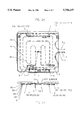
- FIG. 1 is an isometric view of the assembled hot plate oven, including a door in the open position for insertion of a substrate into the oven chamber by a wafer handler such as a robotic arm end effector.
- FIG. 2A is a bottom view of the heater block illustrating the layout of the heating elements with terminations and the central pin.
- FIG. 2B is a side view of the heater block illustrating the terminations of the heating elements and the central pin with its cooling tubes.
- FIG. 3A is a top view of the hot plate oven illustrating the door assembly and the display holding frame.
- FIG. 3B is a side view of the hot plate oven illustrating the door assembly, the substrate raising plate, the display holding frame, the heater block, and the chamber housing.
- FIG. 4A is a front view of the hot plate oven with the door assembly removed.
- a partial cutaway on the left of the drawing illustrates the arrangement of the heater block, the central pin, the display holding frame with a substrate on the frame, the insulation, the housing cover, the spacer rod, and the substrate raising plate.
- FIG. 4B is an enlarged partial cutaway of the left hand side of the front of the oven with the door assembly removed. It illustrates the arrangement of the heater block with its underlying support, the frame, the insulation, the housing cover, the spacer rod, the sealing plate and the substrate raising plate.
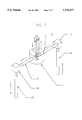
- FIG. 5 illustrates an isolated view of the door assembly with the door in the open position.
- FIG. 6 illustrates the display holding frame by itself for holding a substrate.
- FIG. 7 is an isometric view of the fluid cooled central pin with its associated cooling tubes.
- the invention provides a hot plate oven and a method suitable to bake materials on substrates such as flat panel displays and large semiconductor wafers such as 300 mm in diameter and above.
- baking is done in a hot plate oven after coating the substrate with chemicals such as photoresist (resist) to dry out any solvents and form one or more uniform layers of the material on the top of the substrate.
- chemicals such as photoresist (resist) to dry out any solvents and form one or more uniform layers of the material on the top of the substrate.
- the hot plate oven can be used in conjunction with a vapor prime process such as those used in the semiconductor industry.
- a vapor prime process such as those used in the semiconductor industry.
- a priming agent such as hexamethyldisilane (HMDS) maintained in a liquid phase in a canister.
- HMDS hexamethyldisilane
- nitrogen gas at 5 psig or less is bubbled through the liquid HMDS, and the saturated vapor introduced into the oven chamber for less than a few minutes under a vacuum such as 15 inches of Hg.
- Introduction of the saturated vapor of nitrogen and HMDS is then stopped and pure nitrogen is supplied to purge the oven chamber while the chamber is exhausted.
- the vapor prime process is believed to provide better adhesion properties between the substrate and resists.
- the oven is maintained at about 150-180 degrees C.
- FIG. 1 is an isometric view of the assembled hot plate oven 70.
- the hot plate oven 70 includes a door 40, shown in the open position, for entry of a wafer handler such as robotic arm end effector 67 to bring a substrate 69 into a oven chamber defined by a chamber housing 48 and housing cover 52 where the material on substrate 69 is baked.
- the door 40 is opened and closed by movement of piston rods 72 and 73 within cylinders 35 and 44 (FIG. 3A), respectively.
- the hot plate oven 70 includes a heater block 1 in the chamber housing 48 providing heat to the substrate 69.
- a substrate raising plate 50 can be raised and lowered vertically upon demand by cylinders 55 and 49 (FIG.
- FIG. 3A which in turn raise and lower a display holding frame 29 (FIG. 3B) which suspends the substrate 69 in the chamber housing 48 above the heater block 1 and below the housing cover 52.
- Two manifolds 63 and 64 are in fluid communication with the chamber housing 48 through the back of the oven 70 and supply and/or exhaust gas to the chamber housing 48, or even pull a vacuum from the chamber housing 48 depending on the given process requirements.
- FIG. 2A is a bottom view of the hot plate oven with emphasis on the heater block and layout of the heating elements with their terminations and a central pin.
- the heater block 1 includes a first heating element 74, a second heating element 76, and a third heating element 78 which are resistive heating elements which make contact with the heater block 1 and are disposed in a snake like pattern.
- the heater block 1 can be made of a suitable conductor such as aluminum.
- the first heating element 74 includes terminations 6 and 7, the second heating element 76 includes terminations 9 and 10, and the third heating element 78 terminations 5 and 8.
- a first power supply wire 2 connects to termination 10 of the second heating element 74 and termination 6 of the third heating element 78.
- a second power supply wire 3 connects to termination 5 of the third heating element 78 and termination 6 of the first heating element 74.
- a third power supply wire 4 connects to termination 6 and 7 of the first heating element 74.
- Power is supplied to the power supply wires 2, 3, and 4 from 208 V three phase AC source.
- the heating elements 74, 76, and 78 and the wires 2, 3, and 4 are insulated where they are exposed and non-insulated in the heater block 1.
- a central pin 11 is disposed in a central region of the heater block 1 and is held in place by screws into the heater block 1. In an alternative embodiment, the central pin 11 may include more than one central pin, and need not be restricted to being disposed at the center of the heater block 1. The central pin 11 only needs to be disposed in the heater block 1 so as to function to counteract any sag of the substrate 69 during the baking process.
- FIG. 2B is a side view of the heater block 1 illustrating the terminations 5, 6, 7, and 8 of the heating elements and the central pin 11 with its cooling tubes 14 and 15.
- Termination 8 includes a heating element 78 (FIG. 2A) which ends in a threaded post 80. Nuts 82 and 83 secure the power supply wire lug 84 to the heating element 78.
- the other terminations 5, 6, and 7 shown in FIG. 2B and terminations 9 and 10 shown in FIG. 2A are of similar construction to termination 8, and lie parallel to the plane of the heater block 1.
- the hot plate oven 70 is a low profile oven capable of being stacked in a multiple oven assembly.
- a cooling fluid such as water is supplied to the cooling tubes 14 and 15 of the central pin 11 to carry heat from the central pin 11 to maintain the central pin 11 at a lower temperature than the heater block 1.
- the central pin 11 prevents sagging in the center of the substrate 69 (e.g., flat panel display and the larger wafers) due to thermal expansion during the baking process, prevents an image from appearing on the top of the substrate 69 opposite the contact point of the pin 11, and protects the integrity of the physical characteristics of the coated substrate 69.
- FIG. 3A is a top view of the hot plate oven 70 illustrating the door assembly and the display holding frame 29. To illustrate these features the hot plate oven 70 is shown without the housing cover 52 (FIG. 3B) in place, without the substrate raising plate 50 (FIG. 3B), and with the door 40 in the open position.
- the door assembly includes a door 40 of preferably aluminum having a door seal 39 preferably of a silicone O-ring.
- the door 40 is attached to a shaft 41 held in place by bearings 38 and 68 on the ends of the shaft 41.
- the shaft 41 is connected to lever 37 and lever 42 at each of its ends, which are connected to clevis 36 and 43 which are at the end of the piston rods 72 and 73.
- the hot plate oven 70 is a low profile oven capable of being stacked in a multiple oven assembly.
- the display holding frame 29 with its associated spacer rods 28, 30, and 32, the cylinders 49 and 55 along with the piston rods 115 and 116 and the central pin 11 in the heater block 1 (FIG. 3B) are shown which actuate the raising and lowering of the display holding frame within the hot plate oven.
- the manifolds 63 and 64 extending from the backside of the chamber housing 48 are also shown.
- FIG. 3B is a side view of the hot plate oven 70 illustrating the door assembly, the substrate raising plate 50, the display holding frame 29, the heater block 1, and the chamber housing 48. To illustrate these features the hot plate oven 70 is shown with the housing cover 52 and substrate raising plate 50 in place and with the door 40 in the open position. The details of the door assembly and the manifold 63 are discussed above in connection with FIG. 3A.
- FIG. 3B is a partial cutaway at the back of the chamber housing 48 to illustrate the arrangement of the heater support 56, the heater block 1, the display holding frame 29 above the heater block 1, the insulation 62 lining the chamber housing 48, the housing cover 52, the spacer rod 30, and the substrate raising plate 50. As shown in FIG.
- the display holding frame 29 is attached to spacer rods 28, 30, and 32 which are attached at the other end to the substrate raising plate 50.
- the spacer rods 28, 30, and 32 enter the housing chamber through the seal plates 51, 53, and 54 as shown in FIG. 4A.
- the display holding frame 29 moves up and down when the piston rods 115 and 116 move vertically in their cylinders 49 and 55 as shown in FIG. 3A.
- the resistance temperature devices 65 and 66 enter the housing chamber 48 through the backside of the hot plate oven 70 and monitor the temperature in the heater block 1.
- FIG. 4A is a front view of the hot plate oven 70 with the door assembly removed.
- a partial cutaway on the left of the drawing illustrates the arrangement of the heater block 1, the central pin 11, the display holding frame 29 with a substrate 69 on the display holding frame 29, housing cover 52, the spacer rods 28, 30, and 32, the seal plates 51, 53, and 54, and a substrate raising plate 50.
- the display holding frame 29 includes a stiffener plate 29 which is attached with screws 25 and 27.
- FIG. 4B is an enlarged partial cutaway of the left hand side of the front of the hot plate oven 70 with the door assembly removed. All the parts are as described earlier in connection with FIG. 3B.
- FIG. 4B shows the overlapping joints 58 of the insulation 57, 59, and 62, and the relationship between the seal 61 within the seal plate 51.
- One material suitable for the insulation is any ceramic insulation used in hot plate ovens capable of withstanding damage under high temperatures such as 250 degrees Centigrade.
- FIG. 5 illustrates the door assembly with the door in the open position.
- FIG. 5 shows the isometric view of the oven door and its operating mechanism alone.
- the components of the door assembly were described earlier in connection with FIG. 3A, and can be made of aluminum with the exception of the shaft 41 and the piston rods 72 and 73 which are preferably made of 300 series stainless steel.
- FIG. 6 illustrates the display holding frame 29 of preferably a series 300 stainless steel by itself for clarity.
- the substrate 69 is supported on its edges by the projections 23 extending along the bottom side of the display holding frame 29.
- the spacer rods 28, 30 and 32 are press-fit into the display holding frame 29.
- a cooling tube 31 also of preferably stainless steel is attached by welding to the display holding frame 29 to provide water or nitrogen cooling for the display holding frame 29.
- the stiffener plate 22 connects the two front sides of the frame 29 by means of the screws 24-27 and 18-21, and has adequate clearance to allow the robotic end effector 67 (FIG. 1) to place the substrate 69 on the frame 29.
- FIG. 7 is an isometric view of the fluid cooled central pin 11.
- the central pin 11 has machined in holes for passage of cooling fluid so that the fluid enters travels in a circuit from the bottom to top of the central pin 11 and back to cool the tip of the central pin 11.
- the central pin 11 can be water or nitrogen cooled to maintain the tip of the central pin 11 at around the room temperature.
- thermal shock can be reduced to a minimum when the substrate 69 comes in contact with the central pin 11.
- the cooling fluid enters first through the cooling tube 14, then the fitting 13, then the cooling tube 17, then into the central pin 11, then the tube 17, then the fitting 16, and finally through the tube 15.
- the fluid flow rate and type of fluid can be obviously adjusted to accommodate the process temperature requirements.
Abstract
Description
Claims (1)
Priority Applications (3)
| Application Number | Priority Date | Filing Date | Title |
|---|---|---|---|
| US08/725,282 US5756157A (en) | 1996-10-02 | 1996-10-02 | Method for processing flat panel displays and large wafers |
| JP26179897A JP3971824B2 (en) | 1996-10-02 | 1997-09-26 | Oven for baking a substrate and method for baking a coating material on a substrate |
| US08/938,396 US6091056A (en) | 1996-10-02 | 1997-09-26 | Hot plate oven for processing flat panel displays and large wafers |
Applications Claiming Priority (1)
| Application Number | Priority Date | Filing Date | Title |
|---|---|---|---|
| US08/725,282 US5756157A (en) | 1996-10-02 | 1996-10-02 | Method for processing flat panel displays and large wafers |
Related Child Applications (1)
| Application Number | Title | Priority Date | Filing Date |
|---|---|---|---|
| US08/938,396 Continuation US6091056A (en) | 1996-10-02 | 1997-09-26 | Hot plate oven for processing flat panel displays and large wafers |
Publications (1)
| Publication Number | Publication Date |
|---|---|
| US5756157A true US5756157A (en) | 1998-05-26 |
Family
ID=24913907
Family Applications (2)
| Application Number | Title | Priority Date | Filing Date |
|---|---|---|---|
| US08/725,282 Expired - Lifetime US5756157A (en) | 1996-10-02 | 1996-10-02 | Method for processing flat panel displays and large wafers |
| US08/938,396 Expired - Lifetime US6091056A (en) | 1996-10-02 | 1997-09-26 | Hot plate oven for processing flat panel displays and large wafers |
Family Applications After (1)
| Application Number | Title | Priority Date | Filing Date |
|---|---|---|---|
| US08/938,396 Expired - Lifetime US6091056A (en) | 1996-10-02 | 1997-09-26 | Hot plate oven for processing flat panel displays and large wafers |
Country Status (2)
| Country | Link |
|---|---|
| US (2) | US5756157A (en) |
| JP (1) | JP3971824B2 (en) |
Cited By (7)
| Publication number | Priority date | Publication date | Assignee | Title |
|---|---|---|---|---|
| US6084215A (en) * | 1997-11-05 | 2000-07-04 | Tokyo Electron Limited | Semiconductor wafer holder with spring-mounted temperature measurement apparatus disposed therein |
| US6176023B1 (en) * | 1996-04-03 | 2001-01-23 | Commissariat A L'energie Atomique | Device for transporting flat objects and process for transferring said objects between said device and a processing machine |
| US20040020601A1 (en) * | 2000-02-10 | 2004-02-05 | Applied Materials, Inc. | Process and an integrated tool for low k dielectric deposition including a pecvd capping module |
| US20170282675A1 (en) * | 2015-12-22 | 2017-10-05 | Uber Technologies, Inc. | Thermal reduction system for an autonomous vehicle |
| CN110006228A (en) * | 2019-04-19 | 2019-07-12 | 武汉华星光电半导体显示技术有限公司 | A kind of oven and baking furnace operation method |
| US11126165B2 (en) | 2020-02-11 | 2021-09-21 | Uatc, Llc | Vehicle computing system cooling systems |
| US11430331B2 (en) | 2017-09-08 | 2022-08-30 | Uatc, Llc | Power and thermal management systems and methods for autonomous vehicles |
Families Citing this family (10)
| Publication number | Priority date | Publication date | Assignee | Title |
|---|---|---|---|---|
| US6416318B1 (en) * | 1999-06-16 | 2002-07-09 | Silicon Valley Group, Inc. | Process chamber assembly with reflective hot plate and pivoting lid |
| KR100514256B1 (en) * | 1999-11-30 | 2005-09-15 | 엘지.필립스 엘시디 주식회사 | Method Of Preventing Particle In Chamber |
| US6432207B1 (en) * | 2001-03-07 | 2002-08-13 | Promos Technologies Inc. | Method and structure for baking a wafer |
| EP1399268B1 (en) * | 2001-06-01 | 2012-10-31 | Ulvac, Inc. | Industrial microdeposition system for polymer light emitting diode displays, printed circuit boards and the like |
| US7160105B2 (en) * | 2001-06-01 | 2007-01-09 | Litrex Corporation | Temperature controlled vacuum chuck |
| TW554409B (en) * | 2002-07-16 | 2003-09-21 | Au Optronics Corp | Movable shutter structure of baking apparatus for semiconductor or liquid crystal display industry related process |
| FR2874783B1 (en) * | 2004-08-27 | 2006-12-01 | Jean Oussalem | ELECTRIC FORGE FOR HEATING HORSES A CHEVAL |
| US20080019806A1 (en) * | 2006-07-24 | 2008-01-24 | Nyi Oo Myo | Small footprint modular processing system |
| WO2011030607A1 (en) * | 2009-09-10 | 2011-03-17 | シャープ株式会社 | Drying device |
| US10377126B2 (en) * | 2016-07-19 | 2019-08-13 | General Electric Company | Retaining plates and disposable build plates for additive manufacturing systems |
Family Cites Families (14)
| Publication number | Priority date | Publication date | Assignee | Title |
|---|---|---|---|---|
| US4794217A (en) * | 1985-04-01 | 1988-12-27 | Qing Hua University | Induction system for rapid heat treatment of semiconductor wafers |
| US4830609A (en) * | 1988-06-13 | 1989-05-16 | Motorola, Inc. | Curing oven system for semiconductor devices |
| EP0346815A3 (en) * | 1988-06-13 | 1990-12-19 | Asahi Glass Company Ltd. | Vacuum processing apparatus and transportation system thereof |
| JPH02149402A (en) * | 1988-11-30 | 1990-06-08 | Fujikura Ltd | Process and device for preparing oxide superconductor |
| JP2889926B2 (en) * | 1989-10-20 | 1999-05-10 | 東京エレクトロン株式会社 | Heat treatment method and heat treatment apparatus for substrate |
| US5263264A (en) * | 1990-01-25 | 1993-11-23 | Speedfam Clean System Company Limited | Method and apparatus for drying wet work |
| DE69126724T2 (en) * | 1990-03-19 | 1998-01-15 | Toshiba Kawasaki Kk | Device for vapor phase separation |
| US5060354A (en) * | 1990-07-02 | 1991-10-29 | George Chizinsky | Heated plate rapid thermal processor |
| JPH0777998B2 (en) * | 1991-01-14 | 1995-08-23 | 大日本スクリーン製造株式会社 | Substrate heating device |
| BR9107026A (en) * | 1991-05-08 | 1994-04-19 | Tom Ao Zakrytogo N Proizv | Drying process of a protective polymer coating on a surface of an article, from a solution and device for preparing it |
| US5131460A (en) * | 1991-10-24 | 1992-07-21 | Applied Materials, Inc. | Reducing particulates during semiconductor fabrication |
| JP2622046B2 (en) * | 1991-11-26 | 1997-06-18 | 大日本スクリーン製造株式会社 | Substrate transfer device |
| JPH06177141A (en) * | 1992-12-08 | 1994-06-24 | Toshiba Corp | Heat treatment furnace |
| US5431700A (en) * | 1994-03-30 | 1995-07-11 | Fsi International, Inc. | Vertical multi-process bake/chill apparatus |
-
1996
- 1996-10-02 US US08/725,282 patent/US5756157A/en not_active Expired - Lifetime
-
1997
- 1997-09-26 JP JP26179897A patent/JP3971824B2/en not_active Expired - Fee Related
- 1997-09-26 US US08/938,396 patent/US6091056A/en not_active Expired - Lifetime
Non-Patent Citations (2)
| Title |
|---|
| U.S. Display Consortium Development Agreement effective Jul. 12, 1994; Contract No. RFP 93 4. * |
| U.S. Display Consortium Development Agreement effective Jul. 12, 1994; Contract No. RFP 93-4. |
Cited By (10)
| Publication number | Priority date | Publication date | Assignee | Title |
|---|---|---|---|---|
| US6176023B1 (en) * | 1996-04-03 | 2001-01-23 | Commissariat A L'energie Atomique | Device for transporting flat objects and process for transferring said objects between said device and a processing machine |
| US6084215A (en) * | 1997-11-05 | 2000-07-04 | Tokyo Electron Limited | Semiconductor wafer holder with spring-mounted temperature measurement apparatus disposed therein |
| US20040020601A1 (en) * | 2000-02-10 | 2004-02-05 | Applied Materials, Inc. | Process and an integrated tool for low k dielectric deposition including a pecvd capping module |
| US20170282675A1 (en) * | 2015-12-22 | 2017-10-05 | Uber Technologies, Inc. | Thermal reduction system for an autonomous vehicle |
| US11430331B2 (en) | 2017-09-08 | 2022-08-30 | Uatc, Llc | Power and thermal management systems and methods for autonomous vehicles |
| US11842639B2 (en) | 2017-09-08 | 2023-12-12 | Uatc, Llc | Power and thermal management systems and methods for autonomous vehicles |
| CN110006228A (en) * | 2019-04-19 | 2019-07-12 | 武汉华星光电半导体显示技术有限公司 | A kind of oven and baking furnace operation method |
| US11126165B2 (en) | 2020-02-11 | 2021-09-21 | Uatc, Llc | Vehicle computing system cooling systems |
| US11287806B2 (en) | 2020-02-11 | 2022-03-29 | Uatc, Llc | Vehicle computing system cooling systems |
| US11537106B2 (en) | 2020-02-11 | 2022-12-27 | Uatc, Llc | Vehicle computing system cooling systems |
Also Published As
| Publication number | Publication date |
|---|---|
| JPH10172877A (en) | 1998-06-26 |
| US6091056A (en) | 2000-07-18 |
| JP3971824B2 (en) | 2007-09-05 |
Similar Documents
| Publication | Publication Date | Title |
|---|---|---|
| US5756157A (en) | Method for processing flat panel displays and large wafers | |
| US8196619B2 (en) | Load lock apparatus, processing system and substrate processing method | |
| JP4237939B2 (en) | Vacuum processing equipment with improved substrate heating and cooling | |
| US5778968A (en) | Method for heating or cooling wafers | |
| US7311782B2 (en) | Apparatus for active temperature control of susceptors | |
| US7022948B2 (en) | Chamber for uniform substrate heating | |
| US6841200B2 (en) | Dual wafer load lock | |
| US7313931B2 (en) | Method and device for heat treatment | |
| US6303906B1 (en) | Resistively heated single wafer furnace | |
| JP3380652B2 (en) | Processing equipment | |
| US20070127898A1 (en) | Stacked annealing system | |
| JP3258885B2 (en) | Film processing equipment | |
| US20010040230A1 (en) | Compact gate valve | |
| JP4283914B2 (en) | Dual flat gas auxiliary heating module | |
| JP3253002B2 (en) | Processing equipment | |
| US20170352562A1 (en) | Dodecadon transfer chamber and processing system having the same | |
| CN100593228C (en) | Vacuum processing device and method | |
| JP4471487B2 (en) | Vacuum processing equipment, vacuum processing method | |
| US4981436A (en) | Vertical type heat-treatment apparatus | |
| JPH0737827A (en) | Heat treatment device | |
| US11923212B2 (en) | Apparatus and method for treating substrate | |
| JP3415272B2 (en) | Processing equipment | |
| JP2001093794A (en) | Heat treatment equipment and substrate treatment equipment provided with the heat treatment equipment | |
| KR20230101659A (en) | Support unit and Apparatus for treating a substrate with the unit |
Legal Events
| Date | Code | Title | Description |
|---|---|---|---|
| AS | Assignment |
Owner name: SILICON VALLEY GROUP, CALIFORNIA Free format text: ASSIGNMENT OF ASSIGNORS INTEREST;ASSIGNORS:KANNAN, CHAK D.;WEBER, ADAM JEROME;REEL/FRAME:008427/0498;SIGNING DATES FROM 19961002 TO 19970311 |
|
| STCF | Information on status: patent grant |
Free format text: PATENTED CASE |
|
| AS | Assignment |
Owner name: DARPA, VIRGINIA Free format text: CONFIRMATORY LICENSE;ASSIGNOR:SILICON VALLEY GROUP, INC.;REEL/FRAME:010497/0493 Effective date: 20000111 |
|
| FPAY | Fee payment |
Year of fee payment: 4 |
|
| REMI | Maintenance fee reminder mailed | ||
| CC | Certificate of correction | ||
| AS | Assignment |
Owner name: ASML US, INC., A CORPORATION OF DELAWARE, ARIZONA Free format text: MERGER;ASSIGNORS:SILICON VALLEY GROUP, INC. (CHANGE OF NAME);ASML US, INC. (MERGER);REEL/FRAME:014863/0689 Effective date: 20011101 |
|
| AS | Assignment |
Owner name: ASML HOLDING N.V., A NETHERLAND CORPORATION, NETHE Free format text: CONFIRMATORY LICENSE;ASSIGNOR:ASML US, INC.;REEL/FRAME:015841/0376 Effective date: 20031002 |
|
| FPAY | Fee payment |
Year of fee payment: 8 |
|
| AS | Assignment |
Owner name: ASML US, INC., ARIZONA Free format text: MERGER;ASSIGNOR:SVG LITHOGRAPHY SYSTEMS, INC.;REEL/FRAME:021360/0189 Effective date: 20011231 Owner name: ASML US, LLC, ARIZONA Free format text: CHANGE OF NAME;ASSIGNOR:ASML US, INC.;REEL/FRAME:021360/0088 Effective date: 20021004 Owner name: ASML US, INC., ARIZONA Free format text: MERGER;ASSIGNOR:ASML US, LLC;REEL/FRAME:021360/0092 Effective date: 20021231 |
|
| FEPP | Fee payment procedure |
Free format text: PAYOR NUMBER ASSIGNED (ORIGINAL EVENT CODE: ASPN); ENTITY STATUS OF PATENT OWNER: LARGE ENTITY |
|
| FPAY | Fee payment |
Year of fee payment: 12 |