US5649144A - Apparatus, systems and methods for improving data cache hit rates - Google Patents
Apparatus, systems and methods for improving data cache hit rates Download PDFInfo
- Publication number
- US5649144A US5649144A US08/705,023 US70502396A US5649144A US 5649144 A US5649144 A US 5649144A US 70502396 A US70502396 A US 70502396A US 5649144 A US5649144 A US 5649144A
- Authority
- US
- United States
- Prior art keywords
- address
- cache
- memory
- register
- data
- Prior art date
- Legal status (The legal status is an assumption and is not a legal conclusion. Google has not performed a legal analysis and makes no representation as to the accuracy of the status listed.)
- Expired - Lifetime
Links
Images
Classifications
-
- G—PHYSICS
- G06—COMPUTING; CALCULATING OR COUNTING
- G06F—ELECTRIC DIGITAL DATA PROCESSING
- G06F9/00—Arrangements for program control, e.g. control units
- G06F9/06—Arrangements for program control, e.g. control units using stored programs, i.e. using an internal store of processing equipment to receive or retain programs
- G06F9/30—Arrangements for executing machine instructions, e.g. instruction decode
- G06F9/30003—Arrangements for executing specific machine instructions
- G06F9/3004—Arrangements for executing specific machine instructions to perform operations on memory
- G06F9/30043—LOAD or STORE instructions; Clear instruction
-
- G—PHYSICS
- G06—COMPUTING; CALCULATING OR COUNTING
- G06F—ELECTRIC DIGITAL DATA PROCESSING
- G06F12/00—Accessing, addressing or allocating within memory systems or architectures
- G06F12/02—Addressing or allocation; Relocation
- G06F12/08—Addressing or allocation; Relocation in hierarchically structured memory systems, e.g. virtual memory systems
- G06F12/0802—Addressing of a memory level in which the access to the desired data or data block requires associative addressing means, e.g. caches
- G06F12/0862—Addressing of a memory level in which the access to the desired data or data block requires associative addressing means, e.g. caches with prefetch
-
- G—PHYSICS
- G06—COMPUTING; CALCULATING OR COUNTING
- G06F—ELECTRIC DIGITAL DATA PROCESSING
- G06F2212/00—Indexing scheme relating to accessing, addressing or allocation within memory systems or architectures
- G06F2212/60—Details of cache memory
- G06F2212/6026—Prefetching based on access pattern detection, e.g. stride based prefetch
Definitions
- the present invention relates in general to data processing systems and in particular to apparatus, systems and methods for improving data cache hit rates.
- Modern processing systems frequently use high speed data caches to decrease the time required to transfer data from main memory to associated processing devices.
- a block of data or "cache line” is prefetched from main memory and loaded (encached) in a small high speed data memory or "data cache.”
- a cache line can have a length of one or more operands as desired.
- the particular data block retrieved from main memory is one which the processor has determined most likely includes particular data that the processor will need for an upcoming operation. If the necessary data is found in the encached data block at the time of the operation, the processor need only access the data from the faster cache memory rather than the larger and slower main memory. The resulting reduction in data access time helps reduce the execution time of the programs being run by the processor.
- cache hit rate One of the most significant factors determining the effectiveness of a particular cache design is the percentage of loads which are satisfied by the cache. This percentage is typically referred to as the cache hit rate. As the cycle time of processors becomes faster, and the number of processor cycles needed to access main memory increases, the cache hit rate becomes the dominant factor in determining cache effectiveness. Thus, because of the utility of data caches in improving system operation speed, substantial efforts have been made to improve cache effectiveness through improved cache hit rates.
- a simple sequential hardware prefetch is a common method for improving cache hit rates.
- this method when a request is issued for the last entry in a cache line stored in the cache memory, the next sequential cache line is read from main memory and encached. While this method is very effective at improving the cache hit rate for sequences of memory requests for data with spatial locality, it does not improve the hit rate for request sequences which call for data stored in widely spaced memory locations.
- Software prefetching is another method for improving cache hit rates.
- a cache load instruction is defined which transfers a block of data from memory to the cache.
- the address of this block of data is computed by the processor using a sequence of instructions, and therefore is not restricted to being spatially adjacent in the processor address space to a previous load address.
- software prefetching is effective at improving the cache hit rate for loads of non-sequential sequences of data, it is subject to several drawbacks.
- performance overhead is required to execute the additional instructions needed to compute the prefetch address and execute the prefetch load instruction.
- the additional overhead can offset any performance gain achieved by improved cache hit rate. Although this overhead can be reduced by providing the processor with the ability to execute multiple instructions each cycle, this capability is expensive in terms of processor hardware.
- the software prefetching technique consumes general purpose registers within the processor. This increases the chance of register spills, with any register spills only further slowing system operation.
- Such apparatus, systems and methods should eliminate the problems associated with current systems which rely on spatial locality when prefetching cache lines.
- Such apparatus, systems and methods should allow the retrieval of cache lines located at widely separated or non-sequential locations in the processor address space.
- Such apparatus, systems and methods should employ a minimum of hardware, should minimize the amount of processing overhead required, and should provide access to widely spaced and non-sequential cache lines.
- the principles of the present invention generally provide for improved cache hit rates in processing systems employing a cache memory system. These principles also generally provide for the transfer from main memory to cache memory of a sequence of data blocks or cache lines which may or may not be adjacently located in the main memory address space. Further, the principles of the present invention allow for the generation of prefetch addresses for the encachement of corresponding data without the need to interrupt other memory operations.
- a system which includes means for generating a memory address, and means for presenting the memory address to a cache to retrieve corresponding data from the cache when such data is stored therein and for presenting the memory address to a main memory to retrieve the corresponding data therefrom when such data is not encached in the cache.
- Means are included for adding an offset value to the memory address to obtain a prefetch address.
- Means are also provided for presenting the prefetch address to the main memory in order to retrieve selected data stored therein. The selected data retrieved from the main memory in response to the prefetch address may then be stored in the cache.
- a processing system which includes a processor operable to execute an instruction which generates a memory address and offset select information.
- a multiplexer is included which has a first input coupled to the processor for selectively passing the memory address and the offset select information from the processor to an address interconnect.
- Prefetch generation circuitry is also provided which includes a register file, an adder, and an interconnect.
- the register file includes at least one register for storing an address offset value and is operable to output an address offset value in response to the offset select information provided by the processor.
- the adder includes a first input coupled to the address interconnect and a second input coupled to the register file.
- the adder is operable to add an address offset value output from the register file and a memory address output from the processor to generate a prefetch address.
- the interconnect provided as part of the prefetch address generation circuitry couples the prefetch address from the adder to a second input of the multiplexer, the multiplexer being further operable to selectively pass the prefetch address to the address interconnect.
- a data interconnect is coupled to the processor.
- a cache is also provided which includes a data port coupled to the data interconnect and an address port coupled to the address interconnect. The cache is operable to store data received from the data interconnect and transfer selected information to the processor via the data interconnect in response to an address.
- the processing system additionally includes a memory system having an address port coupled to the address interconnect and a data port coupled to the data interconnect and is operable to transfer data to the cache and/or processor via the data interconnect in response to an address, and is operable to receive data from the processor via the data interconnect.
- a method for improving cache hit rate in a processing system including a memory and a cache.
- a memory address is generated in response to an instruction and then offset to obtain a prefetch address.
- the cache is then addressed with the prefetch address.
- the prefetch address is discarded.
- the memory is addressed with the prefetch address and such data is retrieved from the memory in response.
- the data retrieved from the main memory in response to the prefetch address is then stored in the cache.
- a method for retrieving from memory and encaching a sequence of data.
- a memory address is generated and added to an offset to obtain a first prefetch address.
- a memory is addressed with the first prefetch address to retrieve a first set of data from the memory.
- the first set of data is then encached in a cache memory.
- the offset value is next modified to obtain a second offset value.
- a new memory address is generated and added to the second offset value to obtain a second prefetch address.
- the memory is addressed with the second prefetch address to retrieve a second set of data which is subsequently encached in the cache memory.
- the embodiments of the present invention advantageously eliminate many of the problems associated with current systems which rely on spatial locality when prefetching cache lines.
- the embodiments of the present invention allow for the retrieval of cache lines located at widely separated or non-sequential locations in the processor address space.
- Systems embodying the principles of the present invention employ a minimum of hardware and require a minimum of processor overhead. Further, the required memory bandwidth is minimized and system operating speed maximized since, preferably, prefetching data to cache is only performed when other memory operations are not taking place.
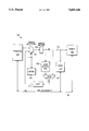
- FIGURE is a functional block diagram of a processing system embodying the principles of the present invention.
- FIG. 1 is a functional block diagram of a processing system 100 embodying the principles of the present invention.
- the primary components of system 100 include a processor 101, a main memory system 102 and a cache memory system 103.
- Processor 101 can be implemented using any one of a number of known architectures; in a preferred embodiment processor 101 is a vector and scalar processor operating on 64-bit wide data words and 32-bit wide addresses.
- Memory system 102 can be of any desired size and can be implemented using any one of a number of available technologies. For example, in the preferred embodiment, memory system 102 is implemented using a plurality of banks of dynamic random access memory devices as described in copending and coassigned patent application Ser. No.
- Cache memory system 103 is also of a known design and has a total size, cache line length, and multi-set associativity selected as required to implement the desired overall design of system 100.
- Addresses from processor 101 are selectively coupled to the address port of main memory 102 and cache 103 through a first port of an address multiplexer 104, an address register 105 and an address interconnect 106.
- Address interconnect 106 may include buses, may be constructed, in whole or in part, as part of a crossbar, or from other suitable interconnection circuitry known in the art.
- Address multiplexer 104 is controlled by processor 101 and associated control circuitry 107. Data is exchanged between processor 101, main memory 102 and cache memory system 103 via a data interconnect 108. Similar to address interconnect 106, data interconnect 108 may include a bus or may be constructed, in whole or in part, as part of a crossbar, or from other suitable interconnection circuitry known in the art.
- system 100 is provided with a stride register file 109, an adder 110 and a queue 111.
- stride register file 109 receives register select information from address register 105 via address interconnect 106 and outputs in response an address offset value stored in a corresponding register therein to a first input port of adder 110.
- a second input port to adder 110 is coupled to address interconnect 106 to directly receive addresses presented on interconnect 106.
- the output of adder 110 (which, as discussed below, is a prefetch address) is coupled back to a second input port of address multiplexer 104 through queue 111.
- Queue 111 may for example hold zero, one or a plurality of prefetch addresses. In alternate embodiments queue 111 is not included and the output of adder 110 is coupled directly to the second input port of multiplexer 104.
- memory request (load) addresses are generated by processor 101 and sent through address multiplexer 104 to address register 105.
- address register 105 a given address is first input by cache system 103 to attempt to retrieve a desired datum from the encached data held therein.
- each datum of a given cache line retrieved from memory 102 is stored in cache 103 along with its associated address.
- the cache system 103 compares the address issued by the processor during a load with those of the encached data. When an address match occurs, the desired data is found in the cache.
- cache 103 If cache 103 contains that datum, cache 103 sends the datum through data interconnect 108 to processor 101. If the cache does not contain the desired datum, the address is sent to main memory 102. Main memory 102 accesses the cache line containing desired datum, and sends it through data interconnect 108 to both processor 101 and cache 103 for encachement.
- processor 101 can execute two new additional types of instructions.
- the first new instruction type directs processor 101 to transfer an integer value to any selected register within stride register file 109. This transfer may be performed through any available interconnect path; in the illustrated embodiment such an integer value may be transferred to register file 109 via address interconnect 106. This integer value operates as an address offset.
- the second new instruction type is a load-with-stride instruction.
- a single one of this second type of instruction directs processor 101 to generate an address to cache 103 to access a desired datum and register select information to select a given stride register within stride register file 109.
- Both the address and stride register selection data are sent through the address multiplexer 104 to address register 105.
- a cache access and a memory access are then performed, as described above.
- the contents of the selected stride register within stride register file 109 are added to the memory address by adder 110 to generate a prefetch address.
- the offset value in alternate embodiments may be subtracted from the memory address to generate the prefetch address for example by using two's complement addition.
- This prefetch address is sent to queue 111, where it can be retained for any desired amount of time.
- queue 111 may be used to hold a prefetch address until a processing cycle when processor 101 is not sending an address to address register 105 such that a prefetch load to cache 103 will never delay processor 101 from initiating other loads and stores.
- prefetch loads discussed further below, are preferably only initiated during unused memory/cache cycles.
- the prefetch address then moves out of queue 111 through the address multiplexer 104 to address register 105, thereby becoming a prefetch load address.
- This prefetch load address is then input by cache 103.
- the prefetch load address is discarded.
- the prefetch address is input by memory system 102.
- Memory system 102 accesses the cache line containing the desired datum, and sends it through the data interconnect 108 to cache 103 for encachement. If this datum arrives in cache 103 before an attempt is made by the processor to load it, then a cache miss is avoided, thereby improving the cache hit rate.
- System 100 advantageously eliminates most of the drawbacks of the prior art. Since a given stride register may contain any address offset, a sequence of cache lines located in memory 102 at either sequential or non-sequential addresses may be correctly prefetched into cache 103. Further, sequences of cache lines separated by varying offsets may also be prefetched by either using multiple stride registers in register file 109 or by varying the contents of a single stride register. In these cases, a sequence of memory addresses from processor 101 may be added to selected offset values from stride register file 109 to obtain a sequence of prefetch addresses, the sequence of prefetch addresses either stepping or jumping through memory 102 to retrieve cache lines.
- prefetch loads are never sent to memory 102 for data already in data cache 103, most of the excess memory bandwidth is eliminated.
- prefetch loads may remain in queue 111 until a cycle where the processor is not sending an address to the address register, prefetch loads will never delay the processor from initiating other loads and stores.
Abstract
Description
Claims (20)
Priority Applications (1)
| Application Number | Priority Date | Filing Date | Title |
|---|---|---|---|
| US08/705,023 US5649144A (en) | 1994-06-13 | 1996-08-29 | Apparatus, systems and methods for improving data cache hit rates |
Applications Claiming Priority (2)
| Application Number | Priority Date | Filing Date | Title |
|---|---|---|---|
| US25879094A | 1994-06-13 | 1994-06-13 | |
| US08/705,023 US5649144A (en) | 1994-06-13 | 1996-08-29 | Apparatus, systems and methods for improving data cache hit rates |
Related Parent Applications (1)
| Application Number | Title | Priority Date | Filing Date |
|---|---|---|---|
| US25879094A Continuation | 1994-06-13 | 1994-06-13 |
Publications (1)
| Publication Number | Publication Date |
|---|---|
| US5649144A true US5649144A (en) | 1997-07-15 |
Family
ID=22982135
Family Applications (1)
| Application Number | Title | Priority Date | Filing Date |
|---|---|---|---|
| US08/705,023 Expired - Lifetime US5649144A (en) | 1994-06-13 | 1996-08-29 | Apparatus, systems and methods for improving data cache hit rates |
Country Status (1)
| Country | Link |
|---|---|
| US (1) | US5649144A (en) |
Cited By (31)
| Publication number | Priority date | Publication date | Assignee | Title |
|---|---|---|---|---|
| WO1999023564A1 (en) | 1997-10-31 | 1999-05-14 | Koninklijke Philips Electronics N.V. | Prefetch management in cache memory |
| US5905999A (en) * | 1996-04-29 | 1999-05-18 | International Business Machines Corporation | Cache sub-array arbitration |
| US5958045A (en) * | 1997-04-02 | 1999-09-28 | Advanced Micro Devices, Inc. | Start of access instruction configured to indicate an access mode for fetching memory operands in a microprocessor |
| WO1999059070A2 (en) * | 1998-05-08 | 1999-11-18 | Koninklijke Philips Electronics N.V. | Data processing circuit with cache memory |
| WO1999064954A2 (en) * | 1998-06-08 | 1999-12-16 | Koninklijke Philips Electronics N.V. | Processor with memory and data prefetch unit |
| US6189094B1 (en) * | 1998-05-27 | 2001-02-13 | Arm Limited | Recirculating register file |
| US6216198B1 (en) * | 1997-09-04 | 2001-04-10 | Nec Corporation | Cache memory accessible for continuous data without tag array indexing |
| JP2001175533A (en) * | 1999-12-14 | 2001-06-29 | Japan Science & Technology Corp | Processor |
| WO2001053934A1 (en) * | 2000-01-18 | 2001-07-26 | Clearwater Networks, Inc. | Method and apparatus for improved computer load and store operations |
| US6311280B1 (en) * | 1999-02-22 | 2001-10-30 | Nband Communications | Low-power memory system with incorporated vector processing |
| SG87041A1 (en) * | 1998-07-01 | 2002-03-19 | Hitachi Ltd | Semiconductor integrated circuit and data processing system |
| US6370634B1 (en) * | 1995-12-22 | 2002-04-09 | Vsevolod Sergeevich Burtsev | Data flow computer with two switches |
| US6401192B1 (en) * | 1998-10-05 | 2002-06-04 | International Business Machines Corporation | Apparatus for software initiated prefetch and method therefor |
| EP1304619A1 (en) * | 2001-10-22 | 2003-04-23 | STMicroelectronics Limited | Cache memory operation |
| US6571318B1 (en) * | 2001-03-02 | 2003-05-27 | Advanced Micro Devices, Inc. | Stride based prefetcher with confidence counter and dynamic prefetch-ahead mechanism |
| US6789100B2 (en) | 1998-12-16 | 2004-09-07 | Mips Technologies, Inc. | Interstream control and communications for multi-streaming digital processors |
| US6848030B2 (en) * | 2001-07-20 | 2005-01-25 | Freescale Semiconductor, Inc. | Method and apparatus for filling lines in a cache |
| US7020879B1 (en) | 1998-12-16 | 2006-03-28 | Mips Technologies, Inc. | Interrupt and exception handling for multi-streaming digital processors |
| US7035997B1 (en) | 1998-12-16 | 2006-04-25 | Mips Technologies, Inc. | Methods and apparatus for improving fetching and dispatch of instructions in multithreaded processors |
| US7237093B1 (en) | 1998-12-16 | 2007-06-26 | Mips Technologies, Inc. | Instruction fetching system in a multithreaded processor utilizing cache miss predictions to fetch instructions from multiple hardware streams |
| US7257814B1 (en) | 1998-12-16 | 2007-08-14 | Mips Technologies, Inc. | Method and apparatus for implementing atomicity of memory operations in dynamic multi-streaming processors |
| US20080229071A1 (en) * | 2007-03-13 | 2008-09-18 | Fujitsu Limited | Prefetch control apparatus, storage device system and prefetch control method |
| US7487296B1 (en) * | 2004-02-19 | 2009-02-03 | Sun Microsystems, Inc. | Multi-stride prefetcher with a recurring prefetch table |
| US7529907B2 (en) | 1998-12-16 | 2009-05-05 | Mips Technologies, Inc. | Method and apparatus for improved computer load and store operations |
| US20090228688A1 (en) * | 2008-03-04 | 2009-09-10 | Qualcomm Incorporated | Dual Function Adder for Computing a Hardware Prefetch Address and an Arithmetic Operation Value |
| US7615857B1 (en) * | 2007-02-14 | 2009-11-10 | Hewlett-Packard Development Company, L.P. | Modular three-dimensional chip multiprocessor |
| US7707391B2 (en) | 1998-12-16 | 2010-04-27 | Mips Technologies, Inc. | Methods and apparatus for improving fetching and dispatch of instructions in multithreaded processors |
| US20120011343A1 (en) * | 2010-07-08 | 2012-01-12 | Seok-In Kim | Data processing apparatus and method |
| US8856452B2 (en) | 2011-05-31 | 2014-10-07 | Illinois Institute Of Technology | Timing-aware data prefetching for microprocessors |
| US20170123985A1 (en) * | 2014-12-14 | 2017-05-04 | Via Alliance Semiconductor Co., Ltd. | Prefetching with level of aggressiveness based on effectiveness by memory access type |
| WO2018028629A1 (en) * | 2016-08-11 | 2018-02-15 | Huawei Technologies Co., Ltd. | Pattern based preload engine |
Citations (8)
| Publication number | Priority date | Publication date | Assignee | Title |
|---|---|---|---|---|
| US4371924A (en) * | 1979-11-09 | 1983-02-01 | Rockwell International Corp. | Computer system apparatus for prefetching data requested by a peripheral device from memory |
| US4583162A (en) * | 1983-01-13 | 1986-04-15 | The Singer Company | Look ahead memory interface |
| US5287487A (en) * | 1990-08-31 | 1994-02-15 | Sun Microsystems, Inc. | Predictive caching method and apparatus for generating a predicted address for a frame buffer |
| US5357618A (en) * | 1991-04-15 | 1994-10-18 | International Business Machines Corporation | Cache prefetch and bypass using stride registers |
| US5361391A (en) * | 1992-06-22 | 1994-11-01 | Sun Microsystems, Inc. | Intelligent cache memory and prefetch method based on CPU data fetching characteristics |
| US5442767A (en) * | 1992-10-23 | 1995-08-15 | International Business Machines Corporation | Address prediction to avoid address generation interlocks in computer systems |
| US5499355A (en) * | 1992-03-06 | 1996-03-12 | Rambus, Inc. | Prefetching into a cache to minimize main memory access time and cache size in a computer system |
| US5581778A (en) * | 1992-08-05 | 1996-12-03 | David Sarnoff Researach Center | Advanced massively parallel computer using a field of the instruction to selectively enable the profiling counter to increase its value in response to the system clock |
-
1996
- 1996-08-29 US US08/705,023 patent/US5649144A/en not_active Expired - Lifetime
Patent Citations (8)
| Publication number | Priority date | Publication date | Assignee | Title |
|---|---|---|---|---|
| US4371924A (en) * | 1979-11-09 | 1983-02-01 | Rockwell International Corp. | Computer system apparatus for prefetching data requested by a peripheral device from memory |
| US4583162A (en) * | 1983-01-13 | 1986-04-15 | The Singer Company | Look ahead memory interface |
| US5287487A (en) * | 1990-08-31 | 1994-02-15 | Sun Microsystems, Inc. | Predictive caching method and apparatus for generating a predicted address for a frame buffer |
| US5357618A (en) * | 1991-04-15 | 1994-10-18 | International Business Machines Corporation | Cache prefetch and bypass using stride registers |
| US5499355A (en) * | 1992-03-06 | 1996-03-12 | Rambus, Inc. | Prefetching into a cache to minimize main memory access time and cache size in a computer system |
| US5361391A (en) * | 1992-06-22 | 1994-11-01 | Sun Microsystems, Inc. | Intelligent cache memory and prefetch method based on CPU data fetching characteristics |
| US5581778A (en) * | 1992-08-05 | 1996-12-03 | David Sarnoff Researach Center | Advanced massively parallel computer using a field of the instruction to selectively enable the profiling counter to increase its value in response to the system clock |
| US5442767A (en) * | 1992-10-23 | 1995-08-15 | International Business Machines Corporation | Address prediction to avoid address generation interlocks in computer systems |
Cited By (66)
| Publication number | Priority date | Publication date | Assignee | Title |
|---|---|---|---|---|
| US6370634B1 (en) * | 1995-12-22 | 2002-04-09 | Vsevolod Sergeevich Burtsev | Data flow computer with two switches |
| US5905999A (en) * | 1996-04-29 | 1999-05-18 | International Business Machines Corporation | Cache sub-array arbitration |
| US5958045A (en) * | 1997-04-02 | 1999-09-28 | Advanced Micro Devices, Inc. | Start of access instruction configured to indicate an access mode for fetching memory operands in a microprocessor |
| US6216198B1 (en) * | 1997-09-04 | 2001-04-10 | Nec Corporation | Cache memory accessible for continuous data without tag array indexing |
| US6134633A (en) * | 1997-10-31 | 2000-10-17 | U.S. Philips Corporation | Prefetch management in cache memory |
| KR100593582B1 (en) * | 1997-10-31 | 2006-06-28 | 코닌클리케 필립스 일렉트로닉스 엔.브이. | Prefetch Management Device in Cache Memory |
| WO1999023564A1 (en) | 1997-10-31 | 1999-05-14 | Koninklijke Philips Electronics N.V. | Prefetch management in cache memory |
| WO1999059070A2 (en) * | 1998-05-08 | 1999-11-18 | Koninklijke Philips Electronics N.V. | Data processing circuit with cache memory |
| US6226715B1 (en) | 1998-05-08 | 2001-05-01 | U.S. Philips Corporation | Data processing circuit with cache memory and cache management unit for arranging selected storage location in the cache memory for reuse dependent on a position of particular address relative to current address |
| WO1999059070A3 (en) * | 1998-05-08 | 2000-03-09 | Koninkl Philips Electronics Nv | Data processing circuit with cache memory |
| US6189094B1 (en) * | 1998-05-27 | 2001-02-13 | Arm Limited | Recirculating register file |
| WO1999064954A3 (en) * | 1998-06-08 | 2000-03-30 | Koninkl Philips Electronics Nv | Processor with memory and data prefetch unit |
| WO1999064954A2 (en) * | 1998-06-08 | 1999-12-16 | Koninklijke Philips Electronics N.V. | Processor with memory and data prefetch unit |
| US6415377B1 (en) | 1998-06-08 | 2002-07-02 | Koninklijke Philips Electronics N.V. | Data processor |
| US7165151B2 (en) | 1998-07-01 | 2007-01-16 | Renesas Technology Corp. | Semiconductor integrated circuit and data processing system |
| US6847578B2 (en) | 1998-07-01 | 2005-01-25 | Renesas Technology Corp. | Semiconductor integrated circuit and data processing system |
| SG87041A1 (en) * | 1998-07-01 | 2002-03-19 | Hitachi Ltd | Semiconductor integrated circuit and data processing system |
| US7254680B2 (en) | 1998-07-01 | 2007-08-07 | Renesas Technology Corp. | Semiconductor integrated circuit and data processing system |
| US20070101088A1 (en) * | 1998-07-01 | 2007-05-03 | Renesas Technology Corp. | Semiconductor intergrated circuit and data processing system |
| US20050099876A1 (en) * | 1998-07-01 | 2005-05-12 | Renesas Technology Corp | Semiconductor integrated circuit and data processing system |
| US6708249B2 (en) | 1998-07-01 | 2004-03-16 | Hitachi, Ltd. | Semiconductor integrated circuit and data processing system |
| US20040114451A1 (en) * | 1998-07-01 | 2004-06-17 | Kazushige Ayukawa | Semiconductor integrated circuit and data processing system |
| US6401192B1 (en) * | 1998-10-05 | 2002-06-04 | International Business Machines Corporation | Apparatus for software initiated prefetch and method therefor |
| US7467385B2 (en) | 1998-12-16 | 2008-12-16 | Mips Technologies, Inc. | Interrupt and exception handling for multi-streaming digital processors |
| US6789100B2 (en) | 1998-12-16 | 2004-09-07 | Mips Technologies, Inc. | Interstream control and communications for multi-streaming digital processors |
| US8468540B2 (en) | 1998-12-16 | 2013-06-18 | Bridge Crossing, Llc | Interrupt and exception handling for multi-streaming digital processors |
| US20050081214A1 (en) * | 1998-12-16 | 2005-04-14 | Nemirovsky Mario D. | Interstream control and communications for multi-streaming digital processors |
| US20110154347A1 (en) * | 1998-12-16 | 2011-06-23 | Nemirovsky Mario D | Interrupt and Exception Handling for Multi-Streaming Digital Processors |
| US7926062B2 (en) | 1998-12-16 | 2011-04-12 | Mips Technologies, Inc. | Interrupt and exception handling for multi-streaming digital processors |
| US7020879B1 (en) | 1998-12-16 | 2006-03-28 | Mips Technologies, Inc. | Interrupt and exception handling for multi-streaming digital processors |
| US7035997B1 (en) | 1998-12-16 | 2006-04-25 | Mips Technologies, Inc. | Methods and apparatus for improving fetching and dispatch of instructions in multithreaded processors |
| US7650605B2 (en) | 1998-12-16 | 2010-01-19 | Mips Technologies, Inc. | Method and apparatus for implementing atomicity of memory operations in dynamic multi-streaming processors |
| US20090125660A1 (en) * | 1998-12-16 | 2009-05-14 | Mips Technologies, Inc. | Interrupt and Exception Handling for Multi-Streaming Digital Processors |
| US20070061619A1 (en) * | 1998-12-16 | 2007-03-15 | Nemirovsky Mario D | Interrupt and exception handling for multi-streaming digital processors |
| US20090241119A1 (en) * | 1998-12-16 | 2009-09-24 | Nemirovsky Mario D | Interrupt and Exception Handling for Multi-Streaming Digital Processors |
| US7237093B1 (en) | 1998-12-16 | 2007-06-26 | Mips Technologies, Inc. | Instruction fetching system in a multithreaded processor utilizing cache miss predictions to fetch instructions from multiple hardware streams |
| US7900207B2 (en) | 1998-12-16 | 2011-03-01 | Mips Technologies, Inc. | Interrupt and exception handling for multi-streaming digital processors |
| US7257814B1 (en) | 1998-12-16 | 2007-08-14 | Mips Technologies, Inc. | Method and apparatus for implementing atomicity of memory operations in dynamic multi-streaming processors |
| US20070294702A1 (en) * | 1998-12-16 | 2007-12-20 | Mips Technologies, Inc. | Method and apparatus for implementing atomicity of memory operations in dynamic multi-streaming processors |
| US7765546B2 (en) | 1998-12-16 | 2010-07-27 | Mips Technologies, Inc. | Interstream control and communications for multi-streaming digital processors |
| US7529907B2 (en) | 1998-12-16 | 2009-05-05 | Mips Technologies, Inc. | Method and apparatus for improved computer load and store operations |
| US7707391B2 (en) | 1998-12-16 | 2010-04-27 | Mips Technologies, Inc. | Methods and apparatus for improving fetching and dispatch of instructions in multithreaded processors |
| US6311280B1 (en) * | 1999-02-22 | 2001-10-30 | Nband Communications | Low-power memory system with incorporated vector processing |
| JP2001175533A (en) * | 1999-12-14 | 2001-06-29 | Japan Science & Technology Corp | Processor |
| WO2001053934A1 (en) * | 2000-01-18 | 2001-07-26 | Clearwater Networks, Inc. | Method and apparatus for improved computer load and store operations |
| US6571318B1 (en) * | 2001-03-02 | 2003-05-27 | Advanced Micro Devices, Inc. | Stride based prefetcher with confidence counter and dynamic prefetch-ahead mechanism |
| US6848030B2 (en) * | 2001-07-20 | 2005-01-25 | Freescale Semiconductor, Inc. | Method and apparatus for filling lines in a cache |
| EP1304619A1 (en) * | 2001-10-22 | 2003-04-23 | STMicroelectronics Limited | Cache memory operation |
| US20040030839A1 (en) * | 2001-10-22 | 2004-02-12 | Stmicroelectronics Limited | Cache memory operation |
| US6959363B2 (en) | 2001-10-22 | 2005-10-25 | Stmicroelectronics Limited | Cache memory operation |
| US7487296B1 (en) * | 2004-02-19 | 2009-02-03 | Sun Microsystems, Inc. | Multi-stride prefetcher with a recurring prefetch table |
| US7811865B2 (en) * | 2007-02-14 | 2010-10-12 | Hewlett-Packard Development Company, L.P. | Method of forming a packaged chip multiprocessor |
| US20100332764A1 (en) * | 2007-02-14 | 2010-12-30 | Norman Paul Jouppi | Modular Three-Dimensional Chip Multiprocessor |
| US20100023692A1 (en) * | 2007-02-14 | 2010-01-28 | Norman Paul Jouppi | Modular three-dimensional chip multiprocessor |
| US7615857B1 (en) * | 2007-02-14 | 2009-11-10 | Hewlett-Packard Development Company, L.P. | Modular three-dimensional chip multiprocessor |
| US8105882B2 (en) | 2007-02-14 | 2012-01-31 | Hewlett-Packard Development Company, L.P. | Processing a memory request in a chip multiprocessor having a stacked arrangement |
| US20080229071A1 (en) * | 2007-03-13 | 2008-09-18 | Fujitsu Limited | Prefetch control apparatus, storage device system and prefetch control method |
| US20090228688A1 (en) * | 2008-03-04 | 2009-09-10 | Qualcomm Incorporated | Dual Function Adder for Computing a Hardware Prefetch Address and an Arithmetic Operation Value |
| US8185721B2 (en) * | 2008-03-04 | 2012-05-22 | Qualcomm Incorporated | Dual function adder for computing a hardware prefetch address and an arithmetic operation value |
| US20120011343A1 (en) * | 2010-07-08 | 2012-01-12 | Seok-In Kim | Data processing apparatus and method |
| US8484437B2 (en) * | 2010-07-08 | 2013-07-09 | Hynix Semiconductor | Data processing apparatus using pre-fetched data |
| US8856452B2 (en) | 2011-05-31 | 2014-10-07 | Illinois Institute Of Technology | Timing-aware data prefetching for microprocessors |
| US20170123985A1 (en) * | 2014-12-14 | 2017-05-04 | Via Alliance Semiconductor Co., Ltd. | Prefetching with level of aggressiveness based on effectiveness by memory access type |
| US10387318B2 (en) * | 2014-12-14 | 2019-08-20 | Via Alliance Semiconductor Co., Ltd | Prefetching with level of aggressiveness based on effectiveness by memory access type |
| WO2018028629A1 (en) * | 2016-08-11 | 2018-02-15 | Huawei Technologies Co., Ltd. | Pattern based preload engine |
| US10248569B2 (en) | 2016-08-11 | 2019-04-02 | Futurewei Technologies, Inc. | Pattern based preload engine |
Similar Documents
| Publication | Publication Date | Title |
|---|---|---|
| US5649144A (en) | Apparatus, systems and methods for improving data cache hit rates | |
| US6185660B1 (en) | Pending access queue for providing data to a target register during an intermediate pipeline phase after a computer cache miss | |
| US5091851A (en) | Fast multiple-word accesses from a multi-way set-associative cache memory | |
| US4933837A (en) | Methods and apparatus for optimizing instruction processing in computer systems employing a combination of instruction cache and high speed consecutive transfer memories | |
| US4888679A (en) | Method and apparatus using a cache and main memory for both vector processing and scalar processing by prefetching cache blocks including vector data elements | |
| US5430888A (en) | Pipeline utilizing an integral cache for transferring data to and from a register | |
| US6317810B1 (en) | Microprocessor having a prefetch cache | |
| EP0667580B1 (en) | Cache System for a memory | |
| EP0604139B1 (en) | Computer system including a prefetch cache | |
| US5561780A (en) | Method and apparatus for combining uncacheable write data into cache-line-sized write buffers | |
| US4701844A (en) | Dual cache for independent prefetch and execution units | |
| JP3518770B2 (en) | Method and apparatus for quickly dispatching instructions to at least one execution unit | |
| JP3425158B2 (en) | Computer system with multi-buffer data cache | |
| JP3516963B2 (en) | Memory access control device | |
| US5996061A (en) | Method for invalidating data identified by software compiler | |
| EP0843261A2 (en) | Virtual channel memory system | |
| US5680631A (en) | Data processor with on-chip cache memory and purge controller responsive to external signal for controlling access to the cache memory | |
| EP0457403A2 (en) | Multilevel instruction cache, method for using said cache, method for compiling instructions for said cache and micro computer system using such a cache | |
| WO1993018459A1 (en) | Prefetching into a cache to minimize main memory access time and cache size in a computer system | |
| JP2002297379A (en) | Hardware prefetch system | |
| CA2283044A1 (en) | An apparatus for software initiated prefetch and method therefor | |
| JPH09160827A (en) | Prefetch of cold cache instruction | |
| US5333291A (en) | Stride enhancer for high speed memory accesses with line fetching mode and normal mode employing boundary crossing determination | |
| EP0279189B1 (en) | Storage system | |
| US5206945A (en) | Single-chip pipeline processor for fetching/flushing instruction/data caches in response to first/second hit/mishit signal respectively detected in corresponding to their logical addresses |
Legal Events
| Date | Code | Title | Description |
|---|---|---|---|
| AS | Assignment |
Owner name: HEWLETT-PACKARD COMPANY, CALIFORNIA Free format text: ASSIGNMENT OF ASSIGNORS INTEREST;ASSIGNOR:CONVEX COMPUTER CORPORATION;REEL/FRAME:008167/0771 Effective date: 19961001 |
|
| STCF | Information on status: patent grant |
Free format text: PATENTED CASE |
|
| FEPP | Fee payment procedure |
Free format text: PAYOR NUMBER ASSIGNED (ORIGINAL EVENT CODE: ASPN); ENTITY STATUS OF PATENT OWNER: LARGE ENTITY |
|
| FPAY | Fee payment |
Year of fee payment: 4 |
|
| AS | Assignment |
Owner name: HEWLETT-PACKARD COMPANY, COLORADO Free format text: MERGER;ASSIGNOR:HEWLETT-PACKARD COMPANY;REEL/FRAME:011523/0469 Effective date: 19980520 |
|
| FPAY | Fee payment |
Year of fee payment: 8 |
|
| FPAY | Fee payment |
Year of fee payment: 12 |
|
| REMI | Maintenance fee reminder mailed | ||
| AS | Assignment |
Owner name: HEWLETT-PACKARD DEVELOPMENT COMPANY, L.P., TEXAS Free format text: ASSIGNMENT OF ASSIGNORS INTEREST;ASSIGNOR:HEWLETT-PACKARD COMPANY;REEL/FRAME:026945/0699 Effective date: 20030131 |