US5643428A - Multiple tier collimator system for enhanced step coverage and uniformity - Google Patents
Multiple tier collimator system for enhanced step coverage and uniformity Download PDFInfo
- Publication number
- US5643428A US5643428A US08/382,366 US38236695A US5643428A US 5643428 A US5643428 A US 5643428A US 38236695 A US38236695 A US 38236695A US 5643428 A US5643428 A US 5643428A
- Authority
- US
- United States
- Prior art keywords
- tier
- collimator
- collimators
- tiers
- target
- Prior art date
- Legal status (The legal status is an assumption and is not a legal conclusion. Google has not performed a legal analysis and makes no representation as to the accuracy of the status listed.)
- Expired - Lifetime
Links
- 239000000758 substrate Substances 0.000 claims abstract description 51
- 238000005240 physical vapour deposition Methods 0.000 claims abstract description 29
- 239000004065 semiconductor Substances 0.000 claims abstract description 11
- 239000002245 particle Substances 0.000 claims description 10
- 235000012431 wafers Nutrition 0.000 abstract description 66
- 238000004544 sputter deposition Methods 0.000 abstract description 11
- 239000010408 film Substances 0.000 description 27
- 238000000151 deposition Methods 0.000 description 23
- 230000008021 deposition Effects 0.000 description 22
- 239000000463 material Substances 0.000 description 9
- 239000010936 titanium Substances 0.000 description 8
- 238000000034 method Methods 0.000 description 7
- -1 aluminum (Al) Chemical class 0.000 description 6
- 230000001965 increasing effect Effects 0.000 description 5
- 230000008569 process Effects 0.000 description 5
- XKRFYHLGVUSROY-UHFFFAOYSA-N argon Substances [Ar] XKRFYHLGVUSROY-UHFFFAOYSA-N 0.000 description 4
- 229910052786 argon Inorganic materials 0.000 description 4
- 239000010949 copper Substances 0.000 description 4
- 238000004519 manufacturing process Methods 0.000 description 4
- 239000013077 target material Substances 0.000 description 4
- 239000002699 waste material Substances 0.000 description 4
- 230000003628 erosive effect Effects 0.000 description 3
- 239000002184 metal Substances 0.000 description 3
- 229910052751 metal Inorganic materials 0.000 description 3
- 238000012545 processing Methods 0.000 description 3
- RYGMFSIKBFXOCR-UHFFFAOYSA-N Copper Chemical compound [Cu] RYGMFSIKBFXOCR-UHFFFAOYSA-N 0.000 description 2
- RTAQQCXQSZGOHL-UHFFFAOYSA-N Titanium Chemical compound [Ti] RTAQQCXQSZGOHL-UHFFFAOYSA-N 0.000 description 2
- 229910045601 alloy Inorganic materials 0.000 description 2
- 239000000956 alloy Substances 0.000 description 2
- 229910052782 aluminium Inorganic materials 0.000 description 2
- XAGFODPZIPBFFR-UHFFFAOYSA-N aluminium Chemical compound [Al] XAGFODPZIPBFFR-UHFFFAOYSA-N 0.000 description 2
- 150000001875 compounds Chemical class 0.000 description 2
- 229910052802 copper Inorganic materials 0.000 description 2
- 230000007423 decrease Effects 0.000 description 2
- 230000000694 effects Effects 0.000 description 2
- 230000001939 inductive effect Effects 0.000 description 2
- 238000010849 ion bombardment Methods 0.000 description 2
- 150000002500 ions Chemical class 0.000 description 2
- 150000002739 metals Chemical class 0.000 description 2
- 230000004044 response Effects 0.000 description 2
- 239000000126 substance Substances 0.000 description 2
- 229910052719 titanium Inorganic materials 0.000 description 2
- 230000010062 adhesion mechanism Effects 0.000 description 1
- 238000013459 approach Methods 0.000 description 1
- 238000007796 conventional method Methods 0.000 description 1
- 238000005137 deposition process Methods 0.000 description 1
- 238000009826 distribution Methods 0.000 description 1
- 230000005684 electric field Effects 0.000 description 1
- 238000005530 etching Methods 0.000 description 1
- 239000007789 gas Substances 0.000 description 1
- 238000012986 modification Methods 0.000 description 1
- 230000004048 modification Effects 0.000 description 1
- 238000005498 polishing Methods 0.000 description 1
- 230000000630 rising effect Effects 0.000 description 1
- 238000006467 substitution reaction Methods 0.000 description 1
- 239000010409 thin film Substances 0.000 description 1
- 238000000427 thin-film deposition Methods 0.000 description 1
- 238000012546 transfer Methods 0.000 description 1
Images


Classifications
-
- H—ELECTRICITY
- H01—ELECTRIC ELEMENTS
- H01J—ELECTRIC DISCHARGE TUBES OR DISCHARGE LAMPS
- H01J37/00—Discharge tubes with provision for introducing objects or material to be exposed to the discharge, e.g. for the purpose of examination or processing thereof
- H01J37/32—Gas-filled discharge tubes
- H01J37/34—Gas-filled discharge tubes operating with cathodic sputtering
- H01J37/3411—Constructional aspects of the reactor
- H01J37/3447—Collimators, shutters, apertures
-
- H—ELECTRICITY
- H01—ELECTRIC ELEMENTS
- H01J—ELECTRIC DISCHARGE TUBES OR DISCHARGE LAMPS
- H01J37/00—Discharge tubes with provision for introducing objects or material to be exposed to the discharge, e.g. for the purpose of examination or processing thereof
- H01J37/32—Gas-filled discharge tubes
- H01J37/34—Gas-filled discharge tubes operating with cathodic sputtering
Definitions
- the present invention is related to currently pending U.S. application Ser. No. 08/316,090, pending, entitled “PVD SPUTTER SYSTEM HAVING NONPLANAR TARGET CONFIGURATION AND METHODS FOR OPERATING SAME" by Krivokapic et al., filed Sep. 30, 1994, which application is incorporated by reference herein in its entirety.
- the present invention is related to currently pending U.S. application Ser. No. 08/316,090, pending, entitled “PVD SPUTTER SYSTEM HAVING NONPLANAR TARGET CONFIGURATION AND METHODS FOR OPERATING SAME" by Krivokapic et al., filed Sep. 30, 1994, which application is incorporated by reference herein in its entirety.
- the invention is generally directed to physical vapor deposition ("PVD") sputter systems.
- the invention is more specifically related to a multiple tier collimator system for use in PVD sputtering during the fabrication of semiconductor devices wherein it is desirable to obtain a combination of uniform deposition thickness, high deposition rate, and good step coverage.
- PVD sputtering is used within semiconductor processing and other arts for depositing metal films and the like onto substrate surfaces.
- the substrate e.g., a semiconductor wafer
- the substrate is typically a planar disk that is positioned, face-down at the top of a vacuum plasma chamber.
- a planar target is further typically positioned face-up within the chamber, in spaced apart and symmetrical counterfacing relation with the substrate.
- the target was on top and the substrate on the bottom.
- the substrate-on-top versus on-bottom orientation relates to keeping the substrate surface clean and is not directly related to the present invention.
- the older configuration with the substrate on the bottom will be shown, but it is to be understood that other orientations are fully within the contemplation of this invention.
- the target is made of the material that is to be sputter deposited onto the substrate surface.
- Examples include, but are not limited to, metals such as aluminum (Al), titanium (Ti), copper (Cu) and alloys or compounds of these materials.
- PVD sputtering involves bombarding the surface of a target material to be deposited as the film with electrostatically accelerated argon ions.
- electric fields are used to accelerate ions in the plasma gas, causing them to impinge on the target surface.
- momentum transfer atoms and electrons are dislodged from the target surface in an area known as the erosion region.
- the dislodged particles follow a generally linear trajectory from their point of emission on the target surface to a collision point on the counterfacing surface of the substrate. Physical adhesion mechanisms cause the target particles to bond to the surface of the substrate, thereby forming a film on the substrate.
- the physical dimensions and positionings of the substrate and target play important roles in determining rate of deposition and the uniformity of the deposited film.
- the distribution of emission-inducing energy across the target also plays a role.
- the target should be very wide relative to the substrate so that the target represents an infinite source plane to the particle-receiving face of the substrate.
- the particle receiving face of the substrate is perfectly planar and parallel to the target, every point on the substrate receiving face will receive the same contribution of deposition particles and film thickness will be uniform across the entire substrate.
- the target has a finite size that is usually the same order of magnitude as that of the substrate.
- Non-uniformities develop across the substrate for characteristics such as deposition film thickness and deposition rate due to boundary conditions.
- Non-uniformities in the substrate may also result from non-uniform target erosion.
- the substrate surface is Often not perfectly planar.
- Nonlinear features such as channels and mesas are typically found on the semiconductor substrate. It is often desirable to coat the sidewalls and/or bottoms of each channel or mesa with a layer of deposition material having a prescribed thickness.
- the linear nature of the trajectories followed by the emitted target particles in PVD systems create shadow effects. Not every portion of the substrate surface receives the same amount of target material at the same rate in the case where the substrate surface includes nonlinearities such as channels or mesas.
- channel is used herein in a broad sense to include features in semiconductor devices and the like such as contact vias, trenches and other depressions which are to be fully or partially filled with deposition material.
- a channel 12 in wafer 10 is shown on FIGS. 1-3.
- mesa is similarly used herein in a broad sense to include any device feature rising above a surrounding plane where the feature and/or its surrounding plane are to be coated with deposition material.
- a mesa 14 in wafer 10 is shown on FIGS. 1-3.
- step coverage is used herein in a qualitative sense to refer to the ability to coat one or more sidewalls or bottom of a channel or mesa to a desired thickness.
- step coverage is further used herein in a quantitative sense to refer to the ratio of film thickness at the bottom center or top center of a channel or mesa, respectively, relative to the general film thickness of the planar regions of the wafer.
- step coverage uniformity is used herein in a quantitative sense to mean the statistical standard deviation (sigma) of step coverage across a given substrate.
- flat coverage uniformity is used herein in a quantitative sense to mean the statistical standard deviation (sigma) of film thickness across a given substrate taking into consideration only substantially planar regions (not step regions) of the substrate surface.
- bottom coverage uniformity is used herein in a quantitative sense to mean the statistical standard deviation (sigma) of film thickness across a given substrate taking into consideration only regions at the bottom of channels or mesas.
- PVD sputtering It is desirable in PVD sputtering to control the path of the sputtered target atoms to travel substantially perpendicularly between the target and the wafer substrate. Perpendicular travel of the target atoms yields an optimal step coverage, i.e., the ratio of film thickness at the bottom or top of channel or mesa, respectively, to film thickness at the planar portions of the wafer.
- One conventional method of controlling the target atom path is by locating collimators within the field between the target and substrate wafer.
- a conventional collimator system 16 including a plurality of collimators is shown in FIG. 1 between a target 18 and a wafer 10.
- a collimator is preferably formed of a plurality of substantially planar surfaces of minimal thickness, which planar surfaces are provided perpendicular to the target and substrate surfaces. With such an orientation, target atoms travelling in substantially perpendicular paths will reach the substrate without contacting a collimator, but target atoms traveling along substantially oblique paths will contact the collimators and be blocked from reaching the wafer substrate.
- a problem with conventional collimator systems is that, while providing good step coverage, they result in poor flat coverage uniformity across the wafer.
- a point P 1 located directly beneath a collimator receives target atoms from a greater surface area of the target, as compared to a point P 2 located between the collimators, because the point P 1 is subject to less blockage, or shadowing, by the collimators than is point P 2 .
- the deposited film tends to have a greater thickness under the collimators than in areas between the collimators. Varying the dimensions of the collimators and distance between the collimator and wafer will vary the location of greatest concentration of target atoms, but areas of disproportionate concentration still occur.
- a desired minimum thickness is to be obtained at point P 2 , for example, an excess amount of material needs to be deposited at P 1 in order to assure that the film thickness at P 2 will be adequate.
- This is disadvantageous because it wastes target material. The target is eroded faster than absolutely necessary and has to be replaced more often. The deposition of excess target material wastes time, energy, and increases the cost of production.
- the excess material near point P 1 has to be polished away or etched back in order to obtain uniform film thickness across the entire surface of the substrate. This also waste time, energy and resources.
- One solution to the problem of poor flat coverage uniformity with collimators is to increase the pressure within the sputtering chamber. Increasing the pressure causes a greater number of collisions between the target atoms as they approach the wafer, and thus the atoms scatter to a greater degree.
- Another solution to the problem of poor flat coverage uniformity with collimators is to increase the distance between the collimators and the wafer substrate. As with increased pressure, the greater distance allows more collisions and greater scattering of the target atoms. Additionally, increasing the distance between the collimators and wafer decreases the blockage or shadow effect that the collimators provide.
- first and second tiers of collimators are provided between a target and wafer substrate.
- the two tiers are preferably hexagonal from a top perspective, spaced from each other, and slightly staggered with respect to each other.
- target atoms are dislodged from the target as result of charged ion particles contacting the surface of the target.
- the dislodged target atoms travel toward the wafer substrate in substantially linear paths.
- the collimator system according to the present invention prevents target atoms from contacting the wafer at substantially oblique angles, thereby providing good step coverage uniformity over the surface of the wafer. Additionally, the presence of more than one tier prevents the localized build-up of target atoms on the wafer that occurs in conventional single tier collimators, thereby providing good flat coverage uniformity over the surface of the wafer.
- the dimensions of the particular collimator tiers and their orientation relative to each other and the wafer may be varied to optimize flat coverage uniformity, step coverage uniformity and film deposition rate. Additionally, the dimensions and relative orientations of the collimator tiers may be controlled to improve either flat coverage uniformity, step coverage uniformity or film deposition rate relative to the other properties.
- FIG. 1 is an exploded perspective view of a conventional collimator system between a target and wafer;
- FIG. 2 is a cross-sectional view through FIG. 1 showing target atom paths from the target to the wafer;
- FIG. 3 is a cross-sectional view similar to FIG. 2 showing a profile of the film thickness deposition on the wafer;
- FIG. 4 is a perspective view of a multiple tier collimator system according to the present invention provided between a target and a wafer;
- FIG. 5 is a top view of the multiple tier collimator system shown in FIG. 4;
- FIG. 6 is a side cross-sectional view of a multiple tier collimator system shown in FIG. 4;
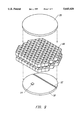
- FIG. 7 is a perspective view of an alternative embodiment of the multiple tier collimator system according to the present invention.
- FIG. 8 is a perspective view of a further embodiment of a multiple tier collimator system according to the present invention.
- FIG. 9 is a perspective view of a further embodiment of a multiple tier collimator system according to the present invention.
- FIGS. 4-9 show various embodiments of a multiple tier collimator system.
- the collimator system of the present invention shall be described herein with regard to PVD sputtering of thin films onto semiconductor wafers.
- the present invention relates specifically to the collimator system.
- Such a system may be used for sputtering films onto substrates other than semiconductor wafers.
- the collimator system according to the present invention may be used in various thin film deposition processes other than PVD sputtering.
- FIGS. 4-6 there is shown a collimator system of the present invention located between a target 30 and a wafer substrate 32.
- FIG. 5 is a top view looking down through the collimator system
- FIG. 6 is a cross-sectional side view through the collimator system.
- target 30 and wafer 32 are generally planar, disc-shaped members oriented generally parallel to and concentric with each other.
- Target 30 is generally of a substantially larger diameter and greater thickness than wafer 32.
- target 30 has a diameter of approximately 300 mm and a thickness of approximately 20 mm.
- the wafer substrate may have a diameter of approximately 200 mm and a thickness of approximately 0.75 mm.
- the shape and size of the wafer 30 and target 32 may vary in alternative embodiments of the present invention. Although only two are shown in FIGS. 4-6, the surface of wafer 32 may include a number of channels 12 and mesas 14 thereon.
- Target 30 may be formed of various materials, including for example, metals such as aluminum (Al), titanium (Ti), copper (Cu) and alloys or compounds of these materials.
- Emission-inducing energy is applied to the active face of the target 30 in the form of, for example, a plasma containing accelerated argon ions.
- a power source (not shown) may be coupled to the target 30 in order to provide the source of the accelerated argon ions.
- confinement magnets (not shown) may also be provided adjacent the target for trapping the argon ions near the surface of the target, to thereby increase ion bombardment of the target.
- target atoms are dislodged from the target and travel linearly away from the target, uniformly distributed about three-dimensional space.
- those target atoms contacting the surface of wafer 32 travel along a substantially perpendicular path between the target and wafer 32.
- Target atoms traveling along a substantially oblique path will result in relatively poor step coverage uniformity across the surface of wafer 32.
- the present invention includes a multiple tier collimator system including a first collimator tier 34 and a second collimator tier 36.
- Collimator tier 34 is comprised of a plurality of collimators 34 i and collimator tier 36 is comprised of a plurality of collimators 36 i .
- a particular collimator 34 i is identical to each of the other collimators in tier 34 and is identical in configuration to each of the collimators 36 i in tier 36.
- a collimator 34 i of collimator tier 34 may have a dissimilar size and/or configuration than other collimators 34 i of collimator tier 34. Additionally, a collimator 34 i of collimator tier 34 may have a dissimilar size and/or configuration than a collimator 36 i of collimator tier 36.
- collimator tiers 34 and 36 are preferably concentric with and larger than wafer 32.
- collimator tiers 34 and 36 may have a radius that is roughly 3 inches greater than that of the wafer 32. Therefore, where the wafer has a diameter of approximately 200 mm, the collimator tiers 34 and 36 may have an approximate diameter of 300 mm. It is understood that the relative sizes of the collimator tiers and the wafer may vary in alternative embodiments provided that the collimator tiers are larger than the wafer.
- Collimators 34 i and 36 i in one embodiment of the present invention have a hexagonal cross-section taken from a perspective perpendicular to the surface of wafer 32.
- the walls separating each of the collimators 34 i and 36 i are preferably as thin as possible, such as for example, 2 mm.
- collimator tier 34 is separated from collimator tier 36 by a distance d 1 (FIG. 6) of 0.5 mm.
- each of the six planner surfaces comprising a particular collimator 34 i in collimator tier 34 may have a width d 2 of 10 mm and a height d 4 of approximately 7 mm.
- each of the six planer surfaces comprising a particular collimator 36 i of collimator tier 36 may have a width d 3 of 10 mm and a height d 5 of 7 mm.
- tier 34 and tier 36 are preferably overlapping but staggered with respect to each other taken from a perspective perpendicular to the surface of wafer 32.
- tier 34 may be staggered by 25% with respect to tier 36.
- the 25% stagger is obtained by moving 25% up along a first, vertical portion of the hexagon and then 25% diagonally across a second, adjacent portion of the hexagon. Therefore, for the above-described dimensions, tier 34 will be offset from tier 36 by a distance d 6 (FIG. 6) equal to 2.5 mm. It is understood that the staggering of one tier with respect to the other my be lesser or greater than 25% in alternative embodiments.
- the bottom collimator 36 may have a lower surface that is spaced a distance d 7 (FIG. 6) of approximately 20 mm away from the surface of wafer 32. While the distance between the target and the upper surface of collimator tier 34 is not as critical as the distance between the wafer 32 and the lower surface of collimator tier 36, the overall distance between target 30 and wafer 32 will affect the deposition rate for the process. Therefore, the distance between the target 30 and the wafer 32 preferably ranges between 50 mm and 100 mm, and the distance between target 30 and an upper surface of collimator tier 34 preferably ranges between 10 mm and 50 mm.
- a multiple tier collimator system having the above described dimensions d 1 through d 7 has been found to yield a film deposition 38 having a particularly good combination of flat coverage uniformity and step coverage uniformity.
- the thickness of film 38 across the surface of wafer 32 is relatively uniform.
- excess deposition of the target was necessary in conventional systems to ensure that each region of the wafer received at least a minimum required film thickness.
- the collimator system according to the present invention makes more efficient use of a target by providing the required minimum film thickness across the entire surface of the wafer without excess film deposition and excess erosion of the target. Similarly, only minimal polishing or etching, if any, is required. Therefore, the present invention provides a saving in time, energy and resources.
- each of the dimensions d 1 through d 7 may be varied in alternative embodiments of the invention, both absolutely and with respect to each other.
- the distance d 1 between collimator tier 34 and collimator tier 36 may vary from 0.5 mm to 5 mm; the width d 2 of a collimator 34 i and width d 3 of a collimator 36 i may vary from 5 mm to 20 mm; and the height d 4 of a collimator 34 i and height d 5 of a collimator 36 i may vary from 5 mm to 20 mm.
- the offset d 6 of collimator tier 34 from collimator tier 36 may vary from 0% to 50% of the width of a collimator 34 i or 36 i , and a lower surface of collimator tier 36 may be located a distance d 7 away from wafer 32 that is between 10 mm and 50 mm.
- d 1 through d 7 Another consideration in providing the dimensions d 1 through d 7 is the rate of deposition of the target on the wafer.
- the rate of deposition of the target on the wafer In general, as d 2 and d 3 increase, the deposition rate increases. As d 4 and d 5 increase, the deposition rate decreases. Therefore, along with step coverage uniformity and flat coverage uniformity, film deposition rate is also a factor relevant to determining the optimal dimensions for the collimators 34 i and 36 i .
- the dimensions of the collimators 34 i and 36 i may be varied to emphasize either step coverage uniformity, flat coverage uniformity, or film deposition rate over the other properties.
- the multiple tier collimator system has been described as having two tiers.
- the present invention may include collimator tiers 40 1 , 40 2 . . . up to 40 n , where in a preferred embodiment n is no greater than 5. It is contemplated, however, that n may be greater than 5 in alternative embodiments.
- the length and width of each of the six planner surfaces comprising a collimator shown in FIG. 7 preferably has the same dimensional ranges as recited above for collimator tiers 34 and 36 described with regard to FIGS. 4-6. Similarly, the spacing between and the offset of adjacent tiers in FIG.
- the lower tier 40 n may have a lower surface that is spaced from the wafer 32 over a range of distances similar to that recited with respect to 7 in FIG. 6.
- collimators comprising the collimator tiers may be formed of shapes other than hexagons.
- FIG. 8 discloses a multiple tier collimator system similar to that shown in FIG. 4, with the exception that the shape of the individual collimators 42 are rectangular when viewed from a perspective perpendicular to the surface of wafer 32.
- FIG. 9 discloses a multiple tier collimator system similar to that disclosed in FIG. 4, with the exception that collimators 44 are triangular when viewed from a perspective perpendicular to the surface of wafer 32.
- collimator tiers may be similar to the dimensional ranges disclosed for collimators 34 i and 36 i described with regard to FIGS. 4-6. It is further understood that the collimator tiers according to the present invention may be comprised of various other geometric shapes when viewed from a perspective perpendicular to the surface of wafer 32. As a further example, a collimator tier may be comprised of a plate with a plurality of circular, or other geometric-shaped, openings formed in the plate. Moreover, it is contemplated that different collimator tiers within a single collimator system may be comprised of different geometric shapes and sizes.
- the collimator system my be comprised of a single tier of collimators having a first group of coplanar collimators interspersed with a second group of coplanar collimators, where the first and second groups reside in different but overlapping planes taken from a perspective parallel to the surface of wafer 32. It is further understood that more than two groups of collimators may be provided to reside in different but overlapping planes. Additionally, more than one tier of collimators may be provided where one or more of the tiers is comprised of groups of collimators that reside in different but overlapping planes.
Abstract
Description
Claims (10)
Priority Applications (5)
| Application Number | Priority Date | Filing Date | Title |
|---|---|---|---|
| US08/382,366 US5643428A (en) | 1995-02-01 | 1995-02-01 | Multiple tier collimator system for enhanced step coverage and uniformity |
| DE69613352T DE69613352T2 (en) | 1995-02-01 | 1996-01-11 | MULTIPLE LAYER COLLIMATOR ARRANGEMENT FOR IMPROVED HEIGHT DIFFERENTIAL COATING AND EVALUATION |
| EP96903508A EP0809859B1 (en) | 1995-02-01 | 1996-01-11 | Multiple tier collimator system for enhanced step coverage and uniformity |
| PCT/US1996/000572 WO1996024155A1 (en) | 1995-02-01 | 1996-01-11 | Multiple tier collimator system for enhanced step coverage and uniformity |
| TW085100804A TW436895B (en) | 1995-02-01 | 1996-01-24 | Multiple tier collimator system for enhanced step coverage and uniformity |
Applications Claiming Priority (1)
| Application Number | Priority Date | Filing Date | Title |
|---|---|---|---|
| US08/382,366 US5643428A (en) | 1995-02-01 | 1995-02-01 | Multiple tier collimator system for enhanced step coverage and uniformity |
Publications (1)
| Publication Number | Publication Date |
|---|---|
| US5643428A true US5643428A (en) | 1997-07-01 |
Family
ID=23508642
Family Applications (1)
| Application Number | Title | Priority Date | Filing Date |
|---|---|---|---|
| US08/382,366 Expired - Lifetime US5643428A (en) | 1995-02-01 | 1995-02-01 | Multiple tier collimator system for enhanced step coverage and uniformity |
Country Status (5)
| Country | Link |
|---|---|
| US (1) | US5643428A (en) |
| EP (1) | EP0809859B1 (en) |
| DE (1) | DE69613352T2 (en) |
| TW (1) | TW436895B (en) |
| WO (1) | WO1996024155A1 (en) |
Cited By (37)
| Publication number | Priority date | Publication date | Assignee | Title |
|---|---|---|---|---|
| US5980702A (en) * | 1994-05-11 | 1999-11-09 | Applied Materials, Inc. | Sputtering apparatus for improved step coverage |
| WO2000008228A1 (en) * | 1998-08-04 | 2000-02-17 | Cvc, Inc. | Dual collimator physical-vapor deposition apparatus |
| US6036821A (en) * | 1998-01-29 | 2000-03-14 | International Business Machines Corporation | Enhanced collimated sputtering apparatus and its method of use |
| US6309515B1 (en) * | 1997-10-29 | 2001-10-30 | Nec Corporation | Sputtering apparatus for sputtering high melting point metal and method for manufacturing semiconductor device having high melting point metal |
| US6362097B1 (en) * | 1998-07-14 | 2002-03-26 | Applied Komatsu Technlology, Inc. | Collimated sputtering of semiconductor and other films |
| US6365134B1 (en) | 1999-07-07 | 2002-04-02 | Scientific Pharmaceuticals, Inc. | Process and composition for high efficacy teeth whitening |
| US6482301B1 (en) | 1998-06-04 | 2002-11-19 | Seagate Technology, Inc. | Target shields for improved magnetic properties of a recording medium |
| US6521897B1 (en) * | 2000-11-17 | 2003-02-18 | The Regents Of The University Of California | Ion beam collimating grid to reduce added defects |
| US20030044360A1 (en) * | 1999-07-07 | 2003-03-06 | Orlowski Jan A. | Process and composition for high efficacy teeth whitening |
| US6596598B1 (en) | 2000-02-23 | 2003-07-22 | Advanced Micro Devices, Inc. | T-shaped gate device and method for making |
| US20030186467A1 (en) * | 2002-03-26 | 2003-10-02 | International Superconductivity Technology Center, The Juridical Foundation | Josephson device and fabrication process thereof |
| US20040086639A1 (en) * | 2002-09-24 | 2004-05-06 | Grantham Daniel Harrison | Patterned thin-film deposition using collimating heated mask asembly |
| US20040202621A1 (en) * | 2002-12-23 | 2004-10-14 | Orlowski Jan A. | Teeth whitening system based on the combination of hydrogen peroxide and carbamide peroxide |
| US20050006223A1 (en) * | 2003-05-07 | 2005-01-13 | Robert Nichols | Sputter deposition masking and methods |
| US20050145477A1 (en) * | 2002-03-19 | 2005-07-07 | Patrick Kaas | Device for targeted application of deposition material to a substrate |
| US20050194545A1 (en) * | 2004-03-08 | 2005-09-08 | Cheng-Shih Lee | [adjustable collimator and sputtering apparatus with the same] |
| US20050214478A1 (en) * | 2004-03-26 | 2005-09-29 | Applied Materials, Inc. | Chemical vapor deposition plasma process using plural ion shower grids |
| US20050211547A1 (en) * | 2004-03-26 | 2005-09-29 | Applied Materials, Inc. | Reactive sputter deposition plasma reactor and process using plural ion shower grids |
| US20060281206A1 (en) * | 2005-06-08 | 2006-12-14 | Advantech Global, Ltd | Shadow mask deposition of materials using reconfigurable shadow masks |
| US20070012559A1 (en) * | 2005-07-13 | 2007-01-18 | Applied Materials, Inc. | Method of improving magnetron sputtering of large-area substrates using a removable anode |
| US7244474B2 (en) | 2004-03-26 | 2007-07-17 | Applied Materials, Inc. | Chemical vapor deposition plasma process using an ion shower grid |
| US20090065349A1 (en) * | 2007-09-06 | 2009-03-12 | Kim Sun-Oo | Plasma Vapor Deposition |
| US7695590B2 (en) | 2004-03-26 | 2010-04-13 | Applied Materials, Inc. | Chemical vapor deposition plasma reactor having plural ion shower grids |
| US7767561B2 (en) | 2004-07-20 | 2010-08-03 | Applied Materials, Inc. | Plasma immersion ion implantation reactor having an ion shower grid |
| US8058156B2 (en) | 2004-07-20 | 2011-11-15 | Applied Materials, Inc. | Plasma immersion ion implantation reactor having multiple ion shower grids |
| US20130180850A1 (en) * | 2010-07-09 | 2013-07-18 | Oc Oerlikon Balzers Ag | Magnetron sputtering apparatus |
| CN103814430A (en) * | 2011-08-17 | 2014-05-21 | 三星电子株式会社 | Sputtering apparatus and method for forming a transmissive conductive layer of a light emitting device |
| USD858468S1 (en) * | 2018-03-16 | 2019-09-03 | Applied Materials, Inc. | Collimator for a physical vapor deposition chamber |
| USD859333S1 (en) * | 2018-03-16 | 2019-09-10 | Applied Materials, Inc. | Collimator for a physical vapor deposition chamber |
| US10640861B2 (en) * | 2015-10-13 | 2020-05-05 | Boe Technology Group Co., Ltd. | Evaporation mask and evaporation device |
| US10777395B2 (en) | 2016-03-14 | 2020-09-15 | Kabushiki Kaisha Toshiba | Processing apparatus and collimator |
| CN112176300A (en) * | 2019-07-02 | 2021-01-05 | Spts科技有限公司 | Deposition apparatus and associated methods |
| USD937329S1 (en) | 2020-03-23 | 2021-11-30 | Applied Materials, Inc. | Sputter target for a physical vapor deposition chamber |
| CN115198236A (en) * | 2021-06-18 | 2022-10-18 | 台湾积体电路制造股份有限公司 | Deposition system and deposition method |
| USD997111S1 (en) | 2021-12-15 | 2023-08-29 | Applied Materials, Inc. | Collimator for use in a physical vapor deposition (PVD) chamber |
| USD998575S1 (en) | 2020-04-07 | 2023-09-12 | Applied Materials, Inc. | Collimator for use in a physical vapor deposition (PVD) chamber |
| USD1009816S1 (en) | 2021-08-29 | 2024-01-02 | Applied Materials, Inc. | Collimator for a physical vapor deposition chamber |
Families Citing this family (6)
| Publication number | Priority date | Publication date | Assignee | Title |
|---|---|---|---|---|
| US5892900A (en) | 1996-08-30 | 1999-04-06 | Intertrust Technologies Corp. | Systems and methods for secure transaction management and electronic rights protection |
| US6157721A (en) | 1996-08-12 | 2000-12-05 | Intertrust Technologies Corp. | Systems and methods using cryptography to protect secure computing environments |
| WO1996027155A2 (en) | 1995-02-13 | 1996-09-06 | Electronic Publishing Resources, Inc. | Systems and methods for secure transaction management and electronic rights protection |
| US6287436B1 (en) | 1998-02-27 | 2001-09-11 | Innovent, Inc. | Brazed honeycomb collimator |
| CN107923036B (en) * | 2016-03-14 | 2020-01-17 | 株式会社东芝 | Processing device and collimator |
| US20210135085A1 (en) * | 2019-11-06 | 2021-05-06 | International Business Machines Corporation | Cluster tool for production-worthy fabrication of dolan bridge quantum josephson junction devices |
Citations (10)
| Publication number | Priority date | Publication date | Assignee | Title |
|---|---|---|---|---|
| US4046359A (en) * | 1976-03-24 | 1977-09-06 | Gellert Jobst U | Injection molding filter assembly |
| US4238685A (en) * | 1978-09-21 | 1980-12-09 | Siemens Aktiengesellschaft | Arrangement for the production of electronic semiconductor components |
| US4824544A (en) * | 1987-10-29 | 1989-04-25 | International Business Machines Corporation | Large area cathode lift-off sputter deposition device |
| US4988424A (en) * | 1989-06-07 | 1991-01-29 | Ppg Industries, Inc. | Mask and method for making gradient sputtered coatings |
| EP0440377A2 (en) * | 1990-01-29 | 1991-08-07 | Varian Associates, Inc. | Collimated deposition apparatus and method |
| US5223108A (en) * | 1991-12-30 | 1993-06-29 | Materials Research Corporation | Extended lifetime collimator |
| EP0606745A1 (en) * | 1992-12-16 | 1994-07-20 | Varian Associates, Inc. | Collimated deposition apparatus |
| US5344352A (en) * | 1992-04-02 | 1994-09-06 | U.S. Philips Corporation | Method of manufacturing a pointed electrode, and device for using said method |
| US5415753A (en) * | 1993-07-22 | 1995-05-16 | Materials Research Corporation | Stationary aperture plate for reactive sputter deposition |
| EP0682125A1 (en) * | 1994-05-11 | 1995-11-15 | Applied Materials, Inc. | Controlling material sputtered from a target |
-
1995
- 1995-02-01 US US08/382,366 patent/US5643428A/en not_active Expired - Lifetime
-
1996
- 1996-01-11 EP EP96903508A patent/EP0809859B1/en not_active Expired - Lifetime
- 1996-01-11 DE DE69613352T patent/DE69613352T2/en not_active Expired - Fee Related
- 1996-01-11 WO PCT/US1996/000572 patent/WO1996024155A1/en active IP Right Grant
- 1996-01-24 TW TW085100804A patent/TW436895B/en active
Patent Citations (12)
| Publication number | Priority date | Publication date | Assignee | Title |
|---|---|---|---|---|
| US4046359A (en) * | 1976-03-24 | 1977-09-06 | Gellert Jobst U | Injection molding filter assembly |
| US4238685A (en) * | 1978-09-21 | 1980-12-09 | Siemens Aktiengesellschaft | Arrangement for the production of electronic semiconductor components |
| US4824544A (en) * | 1987-10-29 | 1989-04-25 | International Business Machines Corporation | Large area cathode lift-off sputter deposition device |
| US4988424A (en) * | 1989-06-07 | 1991-01-29 | Ppg Industries, Inc. | Mask and method for making gradient sputtered coatings |
| EP0440377A2 (en) * | 1990-01-29 | 1991-08-07 | Varian Associates, Inc. | Collimated deposition apparatus and method |
| US5330628A (en) * | 1990-01-29 | 1994-07-19 | Varian Associates, Inc. | Collimated deposition apparatus and method |
| US5223108A (en) * | 1991-12-30 | 1993-06-29 | Materials Research Corporation | Extended lifetime collimator |
| WO1993013542A1 (en) * | 1991-12-30 | 1993-07-08 | Materials Research Corporation | Extended lifetime collimator |
| US5344352A (en) * | 1992-04-02 | 1994-09-06 | U.S. Philips Corporation | Method of manufacturing a pointed electrode, and device for using said method |
| EP0606745A1 (en) * | 1992-12-16 | 1994-07-20 | Varian Associates, Inc. | Collimated deposition apparatus |
| US5415753A (en) * | 1993-07-22 | 1995-05-16 | Materials Research Corporation | Stationary aperture plate for reactive sputter deposition |
| EP0682125A1 (en) * | 1994-05-11 | 1995-11-15 | Applied Materials, Inc. | Controlling material sputtered from a target |
Cited By (58)
| Publication number | Priority date | Publication date | Assignee | Title |
|---|---|---|---|---|
| US5980702A (en) * | 1994-05-11 | 1999-11-09 | Applied Materials, Inc. | Sputtering apparatus for improved step coverage |
| US6309515B1 (en) * | 1997-10-29 | 2001-10-30 | Nec Corporation | Sputtering apparatus for sputtering high melting point metal and method for manufacturing semiconductor device having high melting point metal |
| US6036821A (en) * | 1998-01-29 | 2000-03-14 | International Business Machines Corporation | Enhanced collimated sputtering apparatus and its method of use |
| US6482301B1 (en) | 1998-06-04 | 2002-11-19 | Seagate Technology, Inc. | Target shields for improved magnetic properties of a recording medium |
| US6362097B1 (en) * | 1998-07-14 | 2002-03-26 | Applied Komatsu Technlology, Inc. | Collimated sputtering of semiconductor and other films |
| US6592728B1 (en) * | 1998-08-04 | 2003-07-15 | Veeco-Cvc, Inc. | Dual collimated deposition apparatus and method of use |
| WO2000008228A1 (en) * | 1998-08-04 | 2000-02-17 | Cvc, Inc. | Dual collimator physical-vapor deposition apparatus |
| US6365134B1 (en) | 1999-07-07 | 2002-04-02 | Scientific Pharmaceuticals, Inc. | Process and composition for high efficacy teeth whitening |
| US20030044360A1 (en) * | 1999-07-07 | 2003-03-06 | Orlowski Jan A. | Process and composition for high efficacy teeth whitening |
| US6596598B1 (en) | 2000-02-23 | 2003-07-22 | Advanced Micro Devices, Inc. | T-shaped gate device and method for making |
| US6521897B1 (en) * | 2000-11-17 | 2003-02-18 | The Regents Of The University Of California | Ion beam collimating grid to reduce added defects |
| US20050145477A1 (en) * | 2002-03-19 | 2005-07-07 | Patrick Kaas | Device for targeted application of deposition material to a substrate |
| US7300557B2 (en) * | 2002-03-19 | 2007-11-27 | Scheuten Glasgroep | Device for targeted application of deposition material to a substrate |
| US20030186467A1 (en) * | 2002-03-26 | 2003-10-02 | International Superconductivity Technology Center, The Juridical Foundation | Josephson device and fabrication process thereof |
| US6790675B2 (en) * | 2002-03-26 | 2004-09-14 | International Superconductivity Technology Center | Josephson device and fabrication process thereof |
| US7115168B2 (en) * | 2002-09-24 | 2006-10-03 | Optoelectronic Systems | Patterned thin-film deposition using collimating heated masked assembly |
| US20050183670A1 (en) * | 2002-09-24 | 2005-08-25 | Grantham Daniel H. | Patterned thin-film deposition using collimating heated masked assembly |
| US20040086639A1 (en) * | 2002-09-24 | 2004-05-06 | Grantham Daniel Harrison | Patterned thin-film deposition using collimating heated mask asembly |
| US20040202621A1 (en) * | 2002-12-23 | 2004-10-14 | Orlowski Jan A. | Teeth whitening system based on the combination of hydrogen peroxide and carbamide peroxide |
| US20050006223A1 (en) * | 2003-05-07 | 2005-01-13 | Robert Nichols | Sputter deposition masking and methods |
| US20050194545A1 (en) * | 2004-03-08 | 2005-09-08 | Cheng-Shih Lee | [adjustable collimator and sputtering apparatus with the same] |
| US20050214478A1 (en) * | 2004-03-26 | 2005-09-29 | Applied Materials, Inc. | Chemical vapor deposition plasma process using plural ion shower grids |
| US20050211547A1 (en) * | 2004-03-26 | 2005-09-29 | Applied Materials, Inc. | Reactive sputter deposition plasma reactor and process using plural ion shower grids |
| US7695590B2 (en) | 2004-03-26 | 2010-04-13 | Applied Materials, Inc. | Chemical vapor deposition plasma reactor having plural ion shower grids |
| US7244474B2 (en) | 2004-03-26 | 2007-07-17 | Applied Materials, Inc. | Chemical vapor deposition plasma process using an ion shower grid |
| US7291360B2 (en) | 2004-03-26 | 2007-11-06 | Applied Materials, Inc. | Chemical vapor deposition plasma process using plural ion shower grids |
| US8058156B2 (en) | 2004-07-20 | 2011-11-15 | Applied Materials, Inc. | Plasma immersion ion implantation reactor having multiple ion shower grids |
| US7767561B2 (en) | 2004-07-20 | 2010-08-03 | Applied Materials, Inc. | Plasma immersion ion implantation reactor having an ion shower grid |
| US20070243719A1 (en) * | 2005-06-08 | 2007-10-18 | Advantech Global, Ltd | Shadow mask deposition of materials using reconfigurable shadow masks |
| WO2006133123A2 (en) * | 2005-06-08 | 2006-12-14 | Advantech Global, Ltd. | Shadow mask deposition of materials using reconfigurable shadow masks |
| US7271111B2 (en) * | 2005-06-08 | 2007-09-18 | Advantech Global, Ltd | Shadow mask deposition of materials using reconfigurable shadow masks |
| WO2006133123A3 (en) * | 2005-06-08 | 2007-06-21 | Advantech Global Ltd | Shadow mask deposition of materials using reconfigurable shadow masks |
| US20070246706A1 (en) * | 2005-06-08 | 2007-10-25 | Advantech Global, Ltd | Electronic circuit with repetitive patterns formed by shadow mask vapor deposition and a method of manufacturing an electronic circuit element |
| US7638417B2 (en) | 2005-06-08 | 2009-12-29 | Advantech Global, Ltd | Electronic circuit with repetitive patterns formed by shadow mask vapor deposition and a method of manufacturing an electronic circuit element |
| US7645708B2 (en) | 2005-06-08 | 2010-01-12 | Advantech Global, Ltd | Shadow mask deposition of materials using reconfigurable shadow masks |
| US20100072466A1 (en) * | 2005-06-08 | 2010-03-25 | Advantech Global, Ltd | Electronic Circuit with Repetitive Patterns Formed by Shadow Mask Vapor Deposition and a Method of Manufacturing an Electronic Circuit Element |
| CN101124656B (en) * | 2005-06-08 | 2013-06-19 | 阿德文泰克全球有限公司 | Shadow mask deposition of materials using reconfigurable shadow masks |
| US20100095885A1 (en) * | 2005-06-08 | 2010-04-22 | Advantech Global, Ltd | Shadow Mask Deposition Of Materials Using Reconfigurable Shadow Masks |
| US20060281206A1 (en) * | 2005-06-08 | 2006-12-14 | Advantech Global, Ltd | Shadow mask deposition of materials using reconfigurable shadow masks |
| US7948087B2 (en) | 2005-06-08 | 2011-05-24 | Advantech Global, Ltd | Electronic circuit with repetitive patterns formed by shadow mask vapor deposition and a method of manufacturing an electronic circuit element |
| US8030785B2 (en) | 2005-06-08 | 2011-10-04 | Advantech Global, Ltd | Shadow mask deposition of materials using reconfigurable shadow masks |
| US20070012559A1 (en) * | 2005-07-13 | 2007-01-18 | Applied Materials, Inc. | Method of improving magnetron sputtering of large-area substrates using a removable anode |
| US9194036B2 (en) * | 2007-09-06 | 2015-11-24 | Infineon Technologies Ag | Plasma vapor deposition |
| US20090065349A1 (en) * | 2007-09-06 | 2009-03-12 | Kim Sun-Oo | Plasma Vapor Deposition |
| US20130180850A1 (en) * | 2010-07-09 | 2013-07-18 | Oc Oerlikon Balzers Ag | Magnetron sputtering apparatus |
| US20140197026A1 (en) * | 2011-08-17 | 2014-07-17 | Samsung Electronics Co., Ltd. | Sputtering apparatus and method for forming a transmissive conductive layer of a light emitting device |
| CN103814430A (en) * | 2011-08-17 | 2014-05-21 | 三星电子株式会社 | Sputtering apparatus and method for forming a transmissive conductive layer of a light emitting device |
| US10640861B2 (en) * | 2015-10-13 | 2020-05-05 | Boe Technology Group Co., Ltd. | Evaporation mask and evaporation device |
| US10777395B2 (en) | 2016-03-14 | 2020-09-15 | Kabushiki Kaisha Toshiba | Processing apparatus and collimator |
| USD858468S1 (en) * | 2018-03-16 | 2019-09-03 | Applied Materials, Inc. | Collimator for a physical vapor deposition chamber |
| USD859333S1 (en) * | 2018-03-16 | 2019-09-10 | Applied Materials, Inc. | Collimator for a physical vapor deposition chamber |
| CN112176300A (en) * | 2019-07-02 | 2021-01-05 | Spts科技有限公司 | Deposition apparatus and associated methods |
| USD937329S1 (en) | 2020-03-23 | 2021-11-30 | Applied Materials, Inc. | Sputter target for a physical vapor deposition chamber |
| USD998575S1 (en) | 2020-04-07 | 2023-09-12 | Applied Materials, Inc. | Collimator for use in a physical vapor deposition (PVD) chamber |
| CN115198236A (en) * | 2021-06-18 | 2022-10-18 | 台湾积体电路制造股份有限公司 | Deposition system and deposition method |
| CN115198236B (en) * | 2021-06-18 | 2024-03-08 | 台湾积体电路制造股份有限公司 | Deposition system and deposition method |
| USD1009816S1 (en) | 2021-08-29 | 2024-01-02 | Applied Materials, Inc. | Collimator for a physical vapor deposition chamber |
| USD997111S1 (en) | 2021-12-15 | 2023-08-29 | Applied Materials, Inc. | Collimator for use in a physical vapor deposition (PVD) chamber |
Also Published As
| Publication number | Publication date |
|---|---|
| WO1996024155A1 (en) | 1996-08-08 |
| EP0809859A1 (en) | 1997-12-03 |
| EP0809859B1 (en) | 2001-06-13 |
| TW436895B (en) | 2001-05-28 |
| DE69613352D1 (en) | 2001-07-19 |
| DE69613352T2 (en) | 2002-04-25 |
Similar Documents
| Publication | Publication Date | Title |
|---|---|---|
| US5643428A (en) | Multiple tier collimator system for enhanced step coverage and uniformity | |
| US5556525A (en) | PVD sputter system having nonplanar target configuration and methods for operating same | |
| US5330628A (en) | Collimated deposition apparatus and method | |
| US5650052A (en) | Variable cell size collimator | |
| EP1184483B1 (en) | Thin-film formation system and thin-film formation process | |
| US20200357617A1 (en) | Biasable flux optimizer / collimator for pvd sputter chamber | |
| US4871433A (en) | Method and apparatus for improving the uniformity ion bombardment in a magnetron sputtering system | |
| US5415753A (en) | Stationary aperture plate for reactive sputter deposition | |
| US5242566A (en) | Planar magnetron sputtering source enabling a controlled sputtering profile out to the target perimeter | |
| KR100761592B1 (en) | Contoured sputtering target and method of manufacturing the same | |
| US5658438A (en) | Sputter deposition method for improved bottom and side wall coverage of high aspect ratio features | |
| US5635036A (en) | Collimated deposition apparatus and method | |
| US6592728B1 (en) | Dual collimated deposition apparatus and method of use | |
| KR100221048B1 (en) | Sputtering apparatus | |
| JPS6154111B2 (en) | ||
| US5393398A (en) | Magnetron sputtering apparatus | |
| EP0451642B1 (en) | Sputtering system | |
| TWI573883B (en) | Physical vapor deposition system and physical vapor depositing method using the same | |
| EP0606745B1 (en) | Collimated magnetron sputter-deposition apparatus | |
| JPH08213321A (en) | Uniform film thickness deposition of sputtering material | |
| JP2003027225A (en) | Sputtering target and sputtering system | |
| US6521106B1 (en) | Collimated deposition apparatus | |
| JP3523962B2 (en) | Sputtering apparatus and method for forming thin film by sputtering into hole | |
| US20200051798A1 (en) | Collimator for selective pvd without scanning | |
| US20190353919A1 (en) | Multi-zone collimator for selective pvd |
Legal Events
| Date | Code | Title | Description |
|---|---|---|---|
| AS | Assignment |
Owner name: ADVANCED MICRO DEVICES, INC., CALIFORNIA Free format text: ASSIGNMENT OF ASSIGNORS INTEREST;ASSIGNORS:KRIVOKAPIC, ZORAN;BANG, DAVID S.;REEL/FRAME:007503/0273 Effective date: 19950424 |
|
| STCF | Information on status: patent grant |
Free format text: PATENTED CASE |
|
| FEPP | Fee payment procedure |
Free format text: PAYOR NUMBER ASSIGNED (ORIGINAL EVENT CODE: ASPN); ENTITY STATUS OF PATENT OWNER: LARGE ENTITY |
|
| FPAY | Fee payment |
Year of fee payment: 4 |
|
| FPAY | Fee payment |
Year of fee payment: 8 |
|
| FPAY | Fee payment |
Year of fee payment: 12 |
|
| AS | Assignment |
Owner name: GLOBALFOUNDRIES INC., CAYMAN ISLANDS Free format text: AFFIRMATION OF PATENT ASSIGNMENT;ASSIGNOR:ADVANCED MICRO DEVICES, INC.;REEL/FRAME:023119/0083 Effective date: 20090630 |
|
| AS | Assignment |
Owner name: GLOBALFOUNDRIES U.S. INC., NEW YORK Free format text: RELEASE BY SECURED PARTY;ASSIGNOR:WILMINGTON TRUST, NATIONAL ASSOCIATION;REEL/FRAME:056987/0001 Effective date: 20201117 |