US5631800A - Apparatus for determining operating state of cooling fan - Google Patents
Apparatus for determining operating state of cooling fan Download PDFInfo
- Publication number
- US5631800A US5631800A US08/594,441 US59444196A US5631800A US 5631800 A US5631800 A US 5631800A US 59444196 A US59444196 A US 59444196A US 5631800 A US5631800 A US 5631800A
- Authority
- US
- United States
- Prior art keywords
- cooling fan
- signals
- input terminal
- terminal connected
- output
- Prior art date
- Legal status (The legal status is an assumption and is not a legal conclusion. Google has not performed a legal analysis and makes no representation as to the accuracy of the status listed.)
- Expired - Lifetime
Links
Images


Classifications
-
- G—PHYSICS
- G06—COMPUTING; CALCULATING OR COUNTING
- G06F—ELECTRIC DIGITAL DATA PROCESSING
- G06F1/00—Details not covered by groups G06F3/00 - G06F13/00 and G06F21/00
- G06F1/16—Constructional details or arrangements
- G06F1/20—Cooling means
-
- H—ELECTRICITY
- H02—GENERATION; CONVERSION OR DISTRIBUTION OF ELECTRIC POWER
- H02H—EMERGENCY PROTECTIVE CIRCUIT ARRANGEMENTS
- H02H7/00—Emergency protective circuit arrangements specially adapted for specific types of electric machines or apparatus or for sectionalised protection of cable or line systems, and effecting automatic switching in the event of an undesired change from normal working conditions
- H02H7/08—Emergency protective circuit arrangements specially adapted for specific types of electric machines or apparatus or for sectionalised protection of cable or line systems, and effecting automatic switching in the event of an undesired change from normal working conditions for dynamo-electric motors
- H02H7/093—Emergency protective circuit arrangements specially adapted for specific types of electric machines or apparatus or for sectionalised protection of cable or line systems, and effecting automatic switching in the event of an undesired change from normal working conditions for dynamo-electric motors against increase beyond, or decrease below, a predetermined level of rotational speed
Definitions
- the present invention relates to an apparatus for determining the operating state of a cooling fan, and more particularly, to an apparatus for determining the operating state of a cooling fan used to dissipate heat generated from the operation of a computer system.
- a cooling fan is provided to forcibly discharge the internally generated heat and thereby lower the temperature of the computer system.
- the cooling fan there has been no device for detecting the operating state of the cooling fan in the computer system. If the cooling fan begins to operate in an abnormal condition, or ceases to operate at all, then the internally generated heat cannot be adequately discharged. Therefore, the computer system is at risk of malfunctioning, or incurring serious damage due to the excessive heat.
- the present invention provides an apparatus for detecting an operating state of a cooling fan in a computer system.
- the apparatus includes a pulse generating circuit for generating pulse signals in accordance with the movement of a cooling fan while the cooling fan rotates.
- a per revolution pulse generating circuit generates a pulse signal for every revolution of the cooling fan in accordance with the pulse signals provided from the pulse generating circuit.
- a dividing counter circuit outputs pulse signals having a predetermined period set in accordance with externally received data and reference clock signals.
- a revolution state determining circuit sets a unit time period for checking the operating state of the cooling fan in accordance with the pulse signals provided from the dividing counter circuit.
- the revolution state determining circuit determines the operating state of the cooling fan based on the pulse signals provided from the per revolution pulse generating circuit during the unit time period, and outputs signals for controlling the interrupt state of the computer system when the cooling fan is operating in an abnormal state. Accordingly, further operation of the computer system is prevented when the cooling fan is operating in the abnormal state.
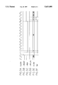
- FIG. 1 is a block diagram showing the apparatus for determining the operating state of a cooling fan in accordance with the principles of the present invention
- FIGS. 2A through 2C illustrate the circuits of the apparatus constructed according to the principles of the present invention
- FIGS. 3A through 3E are timing charts for a first section of a revolution state determining circuit for the cooling fan constructed according to the principles of the present invention
- FIGS. 4A through 4F are timing charts for a second section of the revolution state determining circuit according to the present invention during normal operation.
- FIGS. 5A through 5F are timing charts for the second section of the revolution state determining circuit according to the present invention during abnormal operation.
- the apparatus of FIG. 1 includes a pulse generating circuit 10 for generating pulses in accordance with the movement of a cooling fan while the cooling fan rotates.
- a per revolution pulse generating circuit 20 generates a pulse signal for every revolution of the cooling fan in accordance with the pulse signals provided from pulse generating circuit 10.
- a dividing counter circuit 30 outputs pulse signals having a predetermined period set in accordance with incoming data and reference clock signals CK.
- a revolution state determining circuit 40 sets a unit time period for checking the operating state of the cooling fan in accordance with the pulse signals provided from dividing counter circuit 30.
- Revolution state determining circuit 40 determines the operating state of the cooling fan based on the pulse signals provided from per revolution pulse generating circuit 20 during the unit time period, and outputs signals for controlling the interrupt state of a computer system when the cooling fan is operating in an abnormal condition.
- an abnormal condition is a situation where the cooling fan is either rotating at a speed that is insufficient to properly expel the internally generated heat of the computer system, or is not rotating at all.
- Predetermined operation parameters representative of the rotational speed of the cooling fan that are chosen by the manufacturer can be used to determine whether an abnormal condition exists.
- pulse generating circuit 10 includes a resistor R11 having a first terminal connected to a power source Vcc and a second terminal connected to an anode of a photo diode PD11.
- the cathode of photo diode PD11 is connected to a ground potential.
- a resistor R12 has a first terminal connected to power source Vcc and a second terminal connected to a collector terminal of a photo transistor PT11.
- a photo coupler PC1 is made up of photo diode PD11 and photo transistor PT11. The blades of a cooling fan 15 are interposed between photo diode PD11 and photo transistor PT11.
- a resistor R13 has a first terminal connected to an emitter terminal of photo transistor PT11 and a second terminal connected to a ground potential.
- An invertor G11 has an input terminal connected to the first terminal of resistor R13 and an output terminal connected to an input terminal of an invertor G12.
- Per revolution pulse generating circuit 20 includes a latch 21 for receiving external input signals D through an input terminal in accordance with clock signals LCK1 received through a clock terminal.
- a counter 22 has input terminals D0-D3 connected to output terminals Q0-Q3 of latch 21, and a clock terminal CLK connected to an output terminal of invertor G12 of pulse generating circuit 10.
- An AND gate G21 has a first input terminal connected to receive reset signals -RESET, and a second input terminal connected to a ripple counter terminal -RC of counter 22.
- An output terminal of AND gate G21 is connected to a pre-load terminal PL of counter 22.
- Dividing counter circuit 30 includes a latch 31 for receiving external input signals D through an input terminal, and for receiving clock signals LCK2 through a clock terminal.
- a counter 32 has input terminals D0-D3 connected to output terminals Q0-Q3 of latch 31, and a clock terminal CLK for receiving reference clock signals CK.
- revolution state determining circuit 40 includes a first section 41 for setting a unit time period to determine the operating state of cooling fan 15, and a second section 42 for determining the operating state of cooling fan 15 during the unit time period set by first section 41.
- First section 41 of revolution state determining circuit 40 shown in FIG. 2B includes an AND gate G411 having a first input terminal connected to receive reset signals -RESET, and a second input terminal connected to receive output signals -RHz from an output terminal Q of dividing counter circuit 30.
- An invertor G412 has an input terminal connected to output terminal Q of counter 32 of dividing counter circuit 30.
- An AND gate G413 has one input terminal connected to an output terminal of AND gate G411.
- An AND gate G414 has a first input terminal connected to receive the reset signals -RESET, and a second input terminal connected to an output terminal of invertor G412.
- An AND gate G415 has one input terminal connected to receive reset signals -RESET, and another input terminal connected to the output terminal of invertor G412.
- An OR gate G416 has first through third input terminals connected to output terminals of AND gates G413-G415, respectively.
- a first D flip-flop 411 has an input terminal D1 connected to the output terminal of AND gate G411 and a clock terminal CLK connected to receive clock signals CLOCK.
- First D flip-flop 411 also has an inverting output terminal -Q1 connected to yet another input terminal of AND gate G415.
- a second D flip-flop 412 has an input terminal D2 connected to an output terminal of OR gate G416 and a clock terminal CLK connected to receive clock signals CLOCK.
- Second D flip-flop 412 also has an output terminal Q2 connected to a first input terminal of AND gate G413, and an inverting output terminal -Q2 connected to a third input terminal of AND gate G414.
- An OR gate G417 has first and second input terminals connected to inverting output terminals -Q1 and -Q2 of first and second D flip-flops 411 and 412, respectively.
- Second section 42 of revolution state determining circuit 40 shown in FIG. 2C includes an AND gate G421 having a first input terminal connected to receive reset signals -RESET, and a second input terminal connected to receive output signals -REN from OR gate G417 of the first section 41 of revolution state determining circuit 40 shown in FIG. 2B.
- An invertor G422 has an input terminal connected to receive the output signals -REN from OR gate G417 of the first section 41.
- An invertor G423 has an input terminal connected to receive output signals RPULSE from counter 22 of per revolution pulse generating circuit 20.
- An AND gate G424 has a first input terminal connected to receive reset signals -RESET, a second input terminal connected to an output terminal of invertor G422, and a third input terminal connected to an output terminal of invertor G423.
- An OR gate G425 has one input terminal connected to an output terminal of AND gate G424.
- a second D flip-flop 422 has an input terminal D2 connected to an output terminal of OR gate G425, and a clock terminal CLK connected to receive clock signals CLOCK.
- An AND gate G426 has a first input terminal connected to receive reset signals -RESET, a second input terminal connected to an output terminal of invertor G422, a third input terminal connected to receive output signals -RPULSE from counter 22 of per revolution pulse generating circuit 20, and a fourth input terminal connected to an inverting output terminal of second D flip-flop 422.
- An AND gate G427 has one input terminal connected to an output terminal Q2 of second D flip-flop 422.
- An AND gate G428 has one input terminal connected to the inverting output terminal -Q2 of second D flip-flop 422.
- An OR gate G429 has first and second input terminals connected to output terminals of AND gates G427 and G428, respectively.
- An AND gate G4210 has a first input terminal connected to an output terminal of AND gate G421, a second input terminal connected to an output terminal of OR gate G429, and an output terminal connected to another input terminal of OR gate G425.
- An OR gate G4211 has a first input terminal connected to an output terminal of AND gate G4210 and a second input terminal connected to an output terminal of AND gate G426.
- a first D flip-flop 421 has an input terminal D1 connected to an output terminal of OR gate G4211, and a clock terminal CLK connected to receive clock signals CLOCK.
- First D flip-flop 421 also has an output terminal Q1 connected to another input terminal of AND gate G428, and an inverting output terminal -Q1 connected to another input terminal of AND gate G427 and to a fourth input terminal of AND gate G424.
- An AND gate G4212 has first and second input terminals connected to output terminals Q1 and Q2 of first and second D flip-flops 421 and 422, respectively, and an output terminal for outputting interrupt signals SMI.
- photo coupler PC1 of pulse generating circuit 10 which is formed to detect the blades of cooling fan 15, varies its operating state in accordance with the revolutions of cooling fan 15. That is, when light rays emitted from photo diode PD11 of photo coupler PC1 are shielded by the blades of cooling fan 15, photo transistor PT11 of photo coupler PC1 is maintained in an off state. On the other hand, when the light rays are transmitted from photo diode PD11 to photo transistor PT11 between the blades of cooling fan 15, photo transistor PT11 is switched to an on state.
- photo coupler PC1 of pulse generating circuit 10 repeatedly turns on and off in accordance with the positions of the blades of cooling fan 15, thereby generating pulse signals having a period corresponding to the rotating speed of cooling fan 15. That is, pulse signals NPULSE are output from photo coupler PC1 through invertors G11 and G12 having Schmidt trigger characteristics, and are provided to clock terminal CLK of counter 22 of per revolution pulse generating circuit 20. Per revolution pulse generating circuit 20 generates one pulse for each complete revolution of cooling fan 15 so that the operating state of cooling fan 15 can be determined.
- the number of blades on cooling fan 15 corresponds to the number of input terminals D0-D3 of controller 22, so that relevant data can be provided from output terminals Q0-Q3 of latch 21 in accordance with clock signals LCK1 applied to the clock terminal.
- the data output lines extending from latch 21, which also correspond to the number of blades on cooling fan 15, are connected to input terminals D0-D3 of counter 22, and a high level power source Vcc is provided to an up-down terminal U/D of counter 22. Accordingly, counter 22 operates as a down counter, rather than an up counter.
- Counter 22 executes a down counting operation in accordance with the output signals provided from latch 21 and pulse signals NPULSE provided from pulse generating circuit 10.
- an pulse signal -RPULSE having a specific period is output from terminal TC of counter 22, while an inverted pulse signal is output from ripple counter terminal -RC.
- the inverted pulse signal output from ripple counter terminal -RC is provided to one input terminal of AND gate G21 and the reset signals -RESET are provided to the other input terminal.
- a low level logic signal "L” is input to pre-load terminal PL of counter 22. Therefore, each time the count value become "0", counter 22 is loaded with the output data from latch 21 to execute a new down counting operation.
- counter 22 The operation of counter 22 is executed in the following manner. Each time a number of counts equal to the number of blades on cooling fan 15 is performed, a pulse signal -RPULSE is output from terminal TC. Therefore, for each revolution of cooling fan 15, one pulse is generated and provided to revolution state determining circuit 40.
- Dividing counter circuit 30 divides reference clock signals CK applied to clock terminal CLK of counter 32 by the data provided from latch 31 in accordance with clock signals LCK2, thereby generating pulse signals -RHZ having a specified period. Therefore, during the period of pulse signal -RHZ, which is generated by the operations of latch 31 and counter 32, the operating state of cooling fan 15 of the computer system can be evaluated and determined.
- Latch 31 receives data signals D in accordance with clock signals LCK2, and provides the data signals D through output terminals Q0-Q3 to input terminals D0-D3 of counter 32, which is a programmable dividing counter.
- Counter 32 counts downwardly sequentially in accordance with reference clock signals CK applied to clock terminal CLK.
- Counter 32 then provides pulse signals -RHZ through output terminal Q to revolution state determining circuit 40 in correspondence with the specified period.
- the relevant pulse signals are provided to revolution state determining circuit 40 by the operations of per revolution pulse generating circuit 20 and dividing counter circuit 30.
- Revolution state determining circuit 40 then makes a determination on the rotating condition of cooling fan 15 of the computer system, so that the user can recognize the operating state of cooling fan 15.
- First section 41 of revolution state determining circuit 40 operates based on pulse signals -RHZ provided from dividing counter section 30, and further based on externally provided clock signals CLOCK. First section 41 operates in the following manner.
- Clock signal CLOCK is provided to clock terminals CLK of first and second D flip-flops 411 and 412. If reset signal -RESET for controlling the operation of first section 41 shifts from a low logic level "L” to a high logic level “H”, as shown in FIG. 3B, then the signal -REN output from OR gate G417 shifts logic states, as shown in FIG. 3E, in accordance with the logic states of output terminals Q1 and Q2 of first and second D flip-flops 411 and 412, as shown in FIG. 3D, and in accordance with the pulse signals -RHZ output from dividing counter circuit 30, as shown in FIG. 3C. Accordingly, the signal -REN is provided to second section 42.
- first section 41 of revolution state determining circuit 40 shifts the logic state of output signal -REN, thereby setting the time period (or interval) for checking the operating state of cooling fan 15 of the computer system.
- first section 41 outputs the signal -REN to second section 42 in synchronization with pulse signal -RHZ provided from dividing counter circuit 30, as shown in FIGS. 3C and 3E
- second section 42 makes a determination regarding the operating condition of cooling fan 15 within the set time period using pulse signal -RPULSE provided from per revolution pulse generating circuit 20 and reset signal -RESET.
- Second section 42 of revolution state determining circuit 40 Operation of second section 42 of revolution state determining circuit 40 will now be explained.
- clock signal CLOCK is provided to clock terminals CLK of first and second D flip-flops 421 and 422, as shown in FIGS. 4A and 5A, and reset signal -RESET is shifted to a high logic level "H", as shown in FIGS. 4B and 5B, then the logic state of interrupt signal SMI output from AND gate G4212 can be shifted in accordance with the signal -REN output from first section 41 and pulse signal -RPULSE output from per revolution pulse generating circuit 20.
- interrupt signal SMI output from AND gate G4212 shifts to a high logic level "H", as shown in FIG. 5F, in accordance with the signals provided from output terminals Q1 and Q2 of first and second D flip flops 421 and 422, as shown in FIG. 5E. Therefore, if interrupt signal SMI output from second section 42 exhibits a high logic level "H", then the operation of the computer system is changed to an interrupt state.
- cooling fan 15 of the computer system operates in an abnormal manner, namely, if pulse signal -RPULSE provided from per revolution pulse generating circuit 20 is not output within the time period set by the output signal -REN of first section 41, or if pulse signal -RPULSE is not provided from per revolution pulse generating circuit 20 due to an interruption in the operation of cooling fan 15, then second section 42 of revolution state determining circuit 40 generates interrupt signal SMI to adjust the computer system to an interrupt state.
- interrupt signal SMI output from AND gate H4212 shifts to a high logic level "H"
- the computer system shifts to an interrupt state.
- the current state of the computer system is then stored into an internal memory, and the computer system ceases to operate. Consequently, damage which is likely to occur due to continuous operation of the computer system in spite of the abnormal operating condition of the cooling fan can be prevented.
Landscapes
- Engineering & Computer Science (AREA)
- Theoretical Computer Science (AREA)
- Human Computer Interaction (AREA)
- Physics & Mathematics (AREA)
- General Engineering & Computer Science (AREA)
- General Physics & Mathematics (AREA)
- Cooling Or The Like Of Electrical Apparatus (AREA)
Abstract
Description
Claims (16)
Applications Claiming Priority (2)
| Application Number | Priority Date | Filing Date | Title |
|---|---|---|---|
| KR1019950003701A KR0135898B1 (en) | 1995-02-24 | 1995-02-24 | Fan controlling device |
| KR95-3701 | 1995-02-24 |
Publications (1)
| Publication Number | Publication Date |
|---|---|
| US5631800A true US5631800A (en) | 1997-05-20 |
Family
ID=19408750
Family Applications (1)
| Application Number | Title | Priority Date | Filing Date |
|---|---|---|---|
| US08/594,441 Expired - Lifetime US5631800A (en) | 1995-02-24 | 1996-01-31 | Apparatus for determining operating state of cooling fan |
Country Status (2)
| Country | Link |
|---|---|
| US (1) | US5631800A (en) |
| KR (1) | KR0135898B1 (en) |
Cited By (17)
| Publication number | Priority date | Publication date | Assignee | Title |
|---|---|---|---|---|
| US5834856A (en) * | 1997-08-15 | 1998-11-10 | Compaq Computer Corporation | Computer system comprising a method and apparatus for periodic testing of redundant devices |
| US5835786A (en) * | 1996-05-24 | 1998-11-10 | Micronics Computers Inc. | Computer apparatus with monitoring circuit for displaying fan working condition |
| US5909584A (en) * | 1997-08-15 | 1999-06-01 | Compaq Computer Corp. | Power interlock with fault indicators for computer system |
| US5918059A (en) * | 1997-08-15 | 1999-06-29 | Compaq Computer Corporation | Method and apparatus for responding to actuation of a power supply switch for a computing system |
| US5938751A (en) * | 1997-08-15 | 1999-08-17 | Compaq Computer Corporation | Bus ring-back and voltage over-shoot reduction techniques coupled with hot-pluggability |
| US5951661A (en) * | 1997-08-15 | 1999-09-14 | Compaq Computer Corporation | Bus protocol violation monitor systems and methods |
| US5987538A (en) * | 1997-08-15 | 1999-11-16 | Compaq Computer Corporation | Apparatus for initiating generation of an inter-processor interrupt by a peripheral device not directly connected to any of the multi-processor local interrupt controllers |
| US6000043A (en) * | 1996-06-28 | 1999-12-07 | Intel Corporation | Method and apparatus for management of peripheral devices coupled to a bus |
| US6023402A (en) * | 1998-02-11 | 2000-02-08 | Compact Computer Corporation | Software controlled fan with hardware fail-safe restart |
| US6038633A (en) * | 1997-08-15 | 2000-03-14 | Compaq Computer Corporation | System and method for providing a dual interrupt mechanism to designate the occurrence and termination of an event |
| US6055647A (en) * | 1997-08-15 | 2000-04-25 | Compaq Computer Corporation | Method and apparatus for determining computer system power supply redundancy level |
| US6349385B1 (en) | 1998-11-20 | 2002-02-19 | Compaq Computer Corporation | Dual power supply fan control—thermistor input or software command from the processor |
| US20030099561A1 (en) * | 2001-11-26 | 2003-05-29 | Papst Motoren Gmbh & Co. Kg | Equipment fan |
| US20040232885A1 (en) * | 2000-09-20 | 2004-11-25 | Toshiba Battery Co., Ltd. | Uninterruptible power supply |
| US20050265742A1 (en) * | 2004-05-31 | 2005-12-01 | Samsung Electronics Co., Ltd. | Method for controlling fusing temperature and blower speed based on toner coverage computed from data to be printed and apparatus using the same |
| US20080003008A1 (en) * | 2006-06-30 | 2008-01-03 | Kabushiki Kaisha Toshiba | Fixing unit and fixing temperature control method |
| US7683356B1 (en) * | 2008-10-08 | 2010-03-23 | Hon Hai Precision Industry Co., Ltd. | Voltage converting circuit |
Families Citing this family (2)
| Publication number | Priority date | Publication date | Assignee | Title |
|---|---|---|---|---|
| KR100305563B1 (en) * | 1998-05-27 | 2001-10-29 | 강춘근 | Fan motor driving circuit having computer interface function |
| KR100438534B1 (en) * | 2000-11-28 | 2004-07-03 | 엘지전자 주식회사 | Apparatus of detecting fan failure |
Citations (2)
| Publication number | Priority date | Publication date | Assignee | Title |
|---|---|---|---|---|
| US5130933A (en) * | 1989-09-27 | 1992-07-14 | Zexel Corporation | Rotation sensing system having sensor malfunction detection |
| US5469320A (en) * | 1993-10-29 | 1995-11-21 | Compaq Computer Corp. | Low power fan drive circuit for personal computers |
-
1995
- 1995-02-24 KR KR1019950003701A patent/KR0135898B1/en not_active IP Right Cessation
-
1996
- 1996-01-31 US US08/594,441 patent/US5631800A/en not_active Expired - Lifetime
Patent Citations (2)
| Publication number | Priority date | Publication date | Assignee | Title |
|---|---|---|---|---|
| US5130933A (en) * | 1989-09-27 | 1992-07-14 | Zexel Corporation | Rotation sensing system having sensor malfunction detection |
| US5469320A (en) * | 1993-10-29 | 1995-11-21 | Compaq Computer Corp. | Low power fan drive circuit for personal computers |
Cited By (28)
| Publication number | Priority date | Publication date | Assignee | Title |
|---|---|---|---|---|
| US5835786A (en) * | 1996-05-24 | 1998-11-10 | Micronics Computers Inc. | Computer apparatus with monitoring circuit for displaying fan working condition |
| US6000043A (en) * | 1996-06-28 | 1999-12-07 | Intel Corporation | Method and apparatus for management of peripheral devices coupled to a bus |
| US5987538A (en) * | 1997-08-15 | 1999-11-16 | Compaq Computer Corporation | Apparatus for initiating generation of an inter-processor interrupt by a peripheral device not directly connected to any of the multi-processor local interrupt controllers |
| US5918059A (en) * | 1997-08-15 | 1999-06-29 | Compaq Computer Corporation | Method and apparatus for responding to actuation of a power supply switch for a computing system |
| US5938751A (en) * | 1997-08-15 | 1999-08-17 | Compaq Computer Corporation | Bus ring-back and voltage over-shoot reduction techniques coupled with hot-pluggability |
| US5951661A (en) * | 1997-08-15 | 1999-09-14 | Compaq Computer Corporation | Bus protocol violation monitor systems and methods |
| US5909584A (en) * | 1997-08-15 | 1999-06-01 | Compaq Computer Corp. | Power interlock with fault indicators for computer system |
| US6038633A (en) * | 1997-08-15 | 2000-03-14 | Compaq Computer Corporation | System and method for providing a dual interrupt mechanism to designate the occurrence and termination of an event |
| US6055647A (en) * | 1997-08-15 | 2000-04-25 | Compaq Computer Corporation | Method and apparatus for determining computer system power supply redundancy level |
| US5834856A (en) * | 1997-08-15 | 1998-11-10 | Compaq Computer Corporation | Computer system comprising a method and apparatus for periodic testing of redundant devices |
| US6023402A (en) * | 1998-02-11 | 2000-02-08 | Compact Computer Corporation | Software controlled fan with hardware fail-safe restart |
| US6654894B2 (en) | 1998-11-20 | 2003-11-25 | Hewlett-Packard Development Company, L.P. | Dual control of fan speed-input corresponding to power supply temperature or software command from the processor corresponding to processor temperature |
| US6349385B1 (en) | 1998-11-20 | 2002-02-19 | Compaq Computer Corporation | Dual power supply fan control—thermistor input or software command from the processor |
| US20040232885A1 (en) * | 2000-09-20 | 2004-11-25 | Toshiba Battery Co., Ltd. | Uninterruptible power supply |
| US6998821B2 (en) * | 2000-09-20 | 2006-02-14 | Toshiba Battery Co., Ltd. | Uninterruptible power supply |
| US7352094B2 (en) | 2001-11-26 | 2008-04-01 | Ebm-Papst St. Georgen, Gmbh & Co., Kg | Equipment fan |
| US6864653B2 (en) * | 2001-11-26 | 2005-03-08 | Ebm-Papst St. Georgen Gmbh & Co. Kg | Equipment fan |
| US20030099561A1 (en) * | 2001-11-26 | 2003-05-29 | Papst Motoren Gmbh & Co. Kg | Equipment fan |
| US20050265742A1 (en) * | 2004-05-31 | 2005-12-01 | Samsung Electronics Co., Ltd. | Method for controlling fusing temperature and blower speed based on toner coverage computed from data to be printed and apparatus using the same |
| US7206533B2 (en) | 2004-05-31 | 2007-04-17 | Samsung Electronics Co., Ltd. | Method for controlling fusing temperature and blower speed based on toner coverage computed from data to be printed and apparatus using the same |
| US20080003008A1 (en) * | 2006-06-30 | 2008-01-03 | Kabushiki Kaisha Toshiba | Fixing unit and fixing temperature control method |
| US7729629B2 (en) * | 2006-06-30 | 2010-06-01 | Kabushiki Kaisha Toshiba | Fixing unit and fixing temperature control method |
| US20100202791A1 (en) * | 2006-06-30 | 2010-08-12 | Kabushiki Kaisha Toshiba | Fixing unit and fixing temperature control method |
| US7881631B2 (en) | 2006-06-30 | 2011-02-01 | Kabushiki Kaisha Toshiba | Fixing unit and fixing temperature control method |
| US20110091232A1 (en) * | 2006-06-30 | 2011-04-21 | Kabushiki Kaisha Toshiba | Fixing unit and fixing temperature control method |
| US8036559B2 (en) | 2006-06-30 | 2011-10-11 | Kabushiki Kaisha Toshiba | Fixing unit and fixing temperature control method |
| US7683356B1 (en) * | 2008-10-08 | 2010-03-23 | Hon Hai Precision Industry Co., Ltd. | Voltage converting circuit |
| US20100084543A1 (en) * | 2008-10-08 | 2010-04-08 | Hon Hai Precision Industry Co., Ltd. | Voltage converting circuit |
Also Published As
| Publication number | Publication date |
|---|---|
| KR960032153A (en) | 1996-09-17 |
| KR0135898B1 (en) | 1998-06-15 |
Similar Documents
| Publication | Publication Date | Title |
|---|---|---|
| US5631800A (en) | Apparatus for determining operating state of cooling fan | |
| EP2278432B1 (en) | Adaptive temperature dependent feedback clock control system and method | |
| CA1181478A (en) | Digital speed control for a brushless dc motor | |
| US5367550A (en) | Break address detecting circuit | |
| US20070168686A1 (en) | Method and apparatus for over clocking in a digital processing system | |
| JP2595314B2 (en) | IC card with erroneous writing prevention function | |
| US20020186622A1 (en) | Analog electronic clock | |
| US6188256B1 (en) | Reset-out circuit with feed back capability | |
| US5325341A (en) | Digital timer apparatus and method | |
| US6657501B1 (en) | Instantaneous start up oscillator | |
| US7475295B2 (en) | Intelligent watchdog circuit | |
| US20070164796A1 (en) | Multifunctional timer/event counter device and method of using such a device | |
| JP2001227493A (en) | Fan control circuit | |
| KR19980042799A (en) | Pulse signal generating circuit and pulse signal generating method | |
| EP1419578B1 (en) | Pulse-width modulation with feedback to toggle module | |
| JPH1093426A (en) | High count counter tested freely | |
| US5185770A (en) | Variable frequency dividing circuits | |
| US5333163A (en) | IC including counter circuit and one chip microcomputer thereof | |
| US20050146385A1 (en) | Power-on reset circuit | |
| JP2723748B2 (en) | Timer circuit | |
| US6973353B1 (en) | Programmable controller for controlling an output state | |
| US6530053B1 (en) | Semiconductor device | |
| KR100285313B1 (en) | Apparatus for detecting digital frequency | |
| CN116466638A (en) | Pulse number acquisition equipment and system, pulse signal processing method and device | |
| JPH03251912A (en) | Electronic equipment with system clock switching function |
Legal Events
| Date | Code | Title | Description |
|---|---|---|---|
| AS | Assignment |
Owner name: SAMSUNG ELECTRONICS CO., LTD., A CORP. OF THE REPU Free format text: ASSIGNMENT OF ASSIGNORS INTEREST;ASSIGNORS:JIN, SUNG-KON;HWANG, SEUNG-HWE;REEL/FRAME:007853/0250 Effective date: 19951221 |
|
| STCF | Information on status: patent grant |
Free format text: PATENTED CASE |
|
| FEPP | Fee payment procedure |
Free format text: PAYOR NUMBER ASSIGNED (ORIGINAL EVENT CODE: ASPN); ENTITY STATUS OF PATENT OWNER: LARGE ENTITY |
|
| FPAY | Fee payment |
Year of fee payment: 4 |
|
| FPAY | Fee payment |
Year of fee payment: 8 |
|
| AS | Assignment |
Owner name: JINGPIN TECHNOLOGIES, LLC, DELAWARE Free format text: ASSIGNMENT OF ASSIGNORS INTEREST;ASSIGNOR:SAMSUNG ELECTRONICS CO., LTD.;REEL/FRAME:018883/0845 Effective date: 20070122 |
|
| FEPP | Fee payment procedure |
Free format text: PAYER NUMBER DE-ASSIGNED (ORIGINAL EVENT CODE: RMPN); ENTITY STATUS OF PATENT OWNER: LARGE ENTITY Free format text: PAYOR NUMBER ASSIGNED (ORIGINAL EVENT CODE: ASPN); ENTITY STATUS OF PATENT OWNER: LARGE ENTITY |
|
| FPAY | Fee payment |
Year of fee payment: 12 |