US5604646A - Data error correcting method and signal processing unit for disk accessing apparatus - Google Patents
Data error correcting method and signal processing unit for disk accessing apparatus Download PDFInfo
- Publication number
- US5604646A US5604646A US08/550,840 US55084095A US5604646A US 5604646 A US5604646 A US 5604646A US 55084095 A US55084095 A US 55084095A US 5604646 A US5604646 A US 5604646A
- Authority
- US
- United States
- Prior art keywords
- data
- sync
- disk
- pattern
- buffer
- Prior art date
- Legal status (The legal status is an assumption and is not a legal conclusion. Google has not performed a legal analysis and makes no representation as to the accuracy of the status listed.)
- Expired - Lifetime
Links
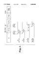
Images


Classifications
-
- G—PHYSICS
- G11—INFORMATION STORAGE
- G11B—INFORMATION STORAGE BASED ON RELATIVE MOVEMENT BETWEEN RECORD CARRIER AND TRANSDUCER
- G11B20/00—Signal processing not specific to the method of recording or reproducing; Circuits therefor
- G11B20/10—Digital recording or reproducing
- G11B20/18—Error detection or correction; Testing, e.g. of drop-outs
- G11B20/1866—Error detection or correction; Testing, e.g. of drop-outs by interleaving
Definitions
- the present invention relates to a method for correcting erroneous data read from a recording medium such as an optical disk or a magnetic disk, and a disk accessing apparatus which can effect the method.
- Disk accessing apparatuses which execute data transfer with recording media such as an optical disk and a magnetic disk, require a fast operational speed.
- One way of increasing the operational speed of a disk accessing apparatus is to increase the operational speed of a signal processing unit provided in the disk accessing apparatus.
- the signal processing unit includes a first-in first-out (FIFO) type speed matching buffer provided between a disk interface and a data transfer unit.
- FIFO first-in first-out
- FIG. 1 is a block diagram of a conventional signal processing unit provided in a disk accessing apparatus for an optical disk.
- the signal processing unit 50 includes an MPU (Micro Processing Unit) interface unit 51, an internal processor 52, a disk interface 53, a host interface 54, an error correcting unit 55 and a data transfer controller 56, which are connected to one another via an internal control bus 58.
- the signal processing unit 50 further includes a speed matching buffer 57.
- the MPU interface unit 51 exchanges control signals with an MPU (not shown) performing the general system control of the disk accessing apparatus.
- the internal processor 52 includes a program ROM (Read Only Memory) 52a, and performs the general control of the signal processing unit 50 in accordance with firmware stored in the program ROM 52a.
- the disk interface 53 is connected to a drive head (not shown) in the disk accessing apparatus.
- the disk interface 53 receives read data D R , i.e., signals read from an optical disk by the drive head. From this read D R , the disk interface 53 reads data in the ID portion in a sector and determines if the sector is the target sector.
- FIG. 2 shows the sector format of an optical disk formatted according to the ISO standards (3.5 inches and single-density capacity).
- Each sector 60 is separated into an ID area 61 and a data area 62.
- the ID area 61 includes a sector mark field, a plurality of lock-up pattern fields, a plurality of address mark fields, a plurality of physical address fields, a postamble field and an optical offset, which are not shown.
- the sector mark field is where a sector mark is to be recorded.
- the lock-up pattern fields are where lock-up patterns are to be recorded.
- the address mark fields are where addresses are to be recorded.
- the physical address fields are where physical addresses are to be recorded.
- the data area 62 includes a plurality of user data fields 62a, a cyclic redundancy check (CRC) field 62b, an error correction code (ECC) field 62c, a sync pattern (SYNC) field 62d, a plurality of resync pattern (RESYNC) fields 62e, a postamble (PA) field 62f and a buffer (BUFF) field 62g.
- the sync pattern field 62d is provided at the head of the data area 62.
- the resync pattern fields 62e are provided among the individual fields 62a, 62b and 62c.
- FIG. 3 presents the detailed illustration of the user data fields 62a, the cyclic redundancy check fields 62b, the error correction code fields 62c, the sync pattern field 62d, and the resync pattern fields 62e.
- the sync pattern field 62d includes three sync patterns SB1, SB2 and SB3. Each of the sync patterns SB1-SB3 consists of one byte.
- the resync pattern fields 62e include thirty-nine resync patterns RS1 to RS39. Each of the resync patterns RS1-RS39 consists of one byte.
- the user data fields 62a each consisting of fifteen bytes are provided between the sync pattern SB3 and the resync pattern RS1 and among the resync patterns RS1-RS34. Groups of fifteen bytes of data D1 to D15, D16 to D30, . . . , and D496 to D510 are recorded in the respective user data fields 62a.
- Recorded between the resync patterns RS34 and RS35 are two bytes of data D511 and D512, four bytes of empty data FF, four bytes of cyclic redundancy check codes CRC1 to CRC4, and ten bytes of error correction codes Ea1 to Ee1 and Ea2 to Ee2.
- the four CRC codes CRC1 to CRC4 comprise the CRC field 62b.
- the ECC fields 62c are provided among the resync patterns RS35 to RS39.
- Each ECC field 62c consists of fifteen one-byte error correction codes.
- sixty one-byte error correction codes Ea3 to Ee3, . . . , and Ea14 to Ee14 are recorded between the resync patterns RS35 and RS39.
- Ten one-byte error correction codes Ea15 to Ee15 and Ea16 to Ee16 are recorded after the last resync pattern RS39.
- eighty error correction codes Ea1 to Ee1, . . . , and Ea16 to Ee16 and five hundred and twelve data D1 to D512 are recorded in one sector.
- each sector 60 The individual patterns, data and codes in each sector 60 are arranged in the direction of the arrow and the top-to-down direction in FIG. 3.
- one vertical line or column of data written in this order is called an "interleave".
- One interleave therefore consists of 120 bytes of data.
- Error correction is carried out for each interleave. Sixteen error correction codes are assigned to each of the interleaves 1 to 5. For example, the error correction codes Ea1 to Ea16 are assigned to interleave 1 and the error correction codes Ed1 to Ed16 are assigned to interleave 4.
- the Reed-Solomon code which exhibits a high correction performance is used for the error correction codes for each interleave, with one byte treated as an element of one code word. It is possible to detect which byte in a single interleave is in error and how it is in error, up to eight bytes (eight pieces of data).
- the Reed-Solomon code on an optical disk treats each element of the code word as an element of a Galois field in byte correction.
- the disk interface 53 detects each data in the ID area 61 in a sector 60 to determine if the sector 60 is the target one.
- the disk interface 53 reads the sync patterns SB1-SB3 and resync patterns RS1-RS39 in the data area 62.
- the disk interface 53 sends subsequently read data D R regarding individual data and codes to the speed matching buffer 57 and the error correcting unit 55.
- the disk interface 53 sends write data D W to be recorded on an optical disk to the drive head in accordance with the aforementioned format.
- the speed matching buffer 57 is a first-in first-out (FIFO) type buffer memory.
- the FIFO buffer 57 has sixteen address areas with a capacity of one byte per address.
- the FIFO buffer 57 receives data from the disk interface 53 byte by byte and sequentially outputs the data to the data transfer controller 56.
- the data transfer controller 56 receives data from the FIFO buffer 57 and stores the data in a buffer memory 59.
- the data and individual codes in one sector 60 which are supplied to the FIFO buffer 57 from the disk interface 53, are also sent to the error correcting unit 55.
- the error correcting unit 55 performs an error correction operation for each interleave.
- the error correction operation for each interleave acquires a syndrome from the entire code word of 120 bytes which constitutes that interleave. Based on this syndrome, it is detected which byte in the interleave is in error and how it is in error.
- the internal processor 52 sends a replacement value to the data transfer controller 56. Based on the replacement value, the data transfer controller 56 corrects the erroneous content of the data and codes which have been previously stored in the buffer memory 59.
- the error-corrected data in the buffer memory 59 is read out to the data transfer controller 56 and is then transferred via the host interface 54 to an external higher rank external unit (not shown).
- the data transfer controller 56 also receives write data D W from the external higher rank unit via the host interface 54 and temporarily stores the write data D W in the buffer memory 59. Thereafter, the data transfer controller 56 reads the write data D W from the buffer memory 59 and sends the write data D W to the disk interface 53 via the FIFO buffer 57.
- This signal processing unit 50 has the FIFO buffer 57 provided between the disk interface 53 and the data transfer controller 56. Even when the data transfer controller 56 performs data transfer with an external higher rank unit using the buffer memory 59, the disk interface 53 can read the read data D R from the optical disk and can write the data read in the FIFO buffer 57. The instance the data transfer process with the external higher rank unit is completed, therefore, the data transfer controller 56 can read data from the FIFO buffer 57 and can transfer it to the buffer memory 59. This allows the signal processing unit 50 to immediately execute the next signal processing operation, thus quickening the signal processing by the signal processing unit 50.
- the disk interface 53 determines that the detection has failed. Then, the disk interface 53 outputs dummy data D D to the FIFO buffer 57.
- the dummy data D D corresponds in number (fifteen) to the data D1 to D15 in the user data field 62a located between the sync patterns SB1-SB3 and the resync pattern RS1.
- Each dummy data D D consists of one byte whose bits are all "0".
- the dummy data D D output to the FIFO buffer 57 is sequentially stored in the buffer memory 59 via the data transfer controller 56.
- the disk interface 53 sequentially outputs the subsequent read data D R i.e., the data in the user data field 62a and the individual codes in the CRC field 62b and the ECC field 62c, to the FIFO buffer 57.
- the data transfer controller 56 reads the data and codes from the FIFO buffer 57 and stores the same in the buffer memory 59.
- the dummy data D D , the data in the user data field 62a and the individual codes in the CRC field 62b and the ECC field 62c are also sent to the error correcting unit 55.
- the error correcting unit 55 executes an operation for error correction for each interleave. In this case, the error correcting unit 55 finds out how many of the whole dummy data D D are in error.
- the internal processor 52 sends a replacement value for each dummy data D D stored in the buffer memory 59 to the data transfer controller 56. Based on the replacement values, the data transfer controller 56 corrects the associated dummy data D D stored in the buffer memory 59.
- This error correction scheme is used in an optical disk accessing apparatus disclosed in Japanese Unexamined Patent Publication No. 1-124158.
- FIG. 4 shows a timing chart for the signal processing unit 50 when reading the sync patterns SB1-SB3 has failed.
- the disk interface 53 When reading the sync patterns SB1-SB3 fails during a detection timing (detection window) T W1 for the sync patterns SB1-SB3, the disk interface 53 outputs dummy data D D . That is, when the detection timing (detection window) T W1 passes and after determining whether or not the reading of the sync patterns has failed, the disk interface 53 outputs the dummy data D D . After the detection timing (detection window) T W1 passes, therefore, the dummy data D D is written in the FIFO buffer 57 with a delay of time T D1 . After a further delay of time T D2 , the dummy data D D is read from the FIFO buffer 57.
- the FIFO buffer 57 has a small capacity, which is generally sixteen (16) bytes. When fifteen (15) bytes of dummy data D D are written in the FIFO buffer 57, the remaining capacity is just one (1) byte. Therefore, when the dummy data D D is written in the FIFO buffer 57 with a delay of time T D1 , a time T D3 from the beginning of the writing of the dummy data D D into the FIFO buffer 57 to the beginning of the writing of the data D16-D30 in the user data field 62a, (following the next resync pattern RS1 read out), becomes shorter.
- T W2 is the detection timing (detection window) for the resync pattern RS1
- T D4 is the time from the beginning of the writing of the data D16-D30 to the beginning of the reading thereof.
- the present invention relates to a data error correcting method that shortens the amount of processing time needed to perform after error correction when reading sync patterns has failed.
- the error correcting method according to the invention can, for example, be implemented as a signal processing unit for a disk accessing apparatus.
- a data error correcting method includes the steps of: A) using a disk accessing apparatus including a drive head, a speed matching buffer and a buffer memory; B) loading read data from a disk as a recording medium by the drive head; C) detecting or identifying a sync pattern in the read data; D) sequentially reading target data following the sync pattern to temporally store the target data to the speed matching buffer; E) transferring the target data stored in the speed matching buffer to the buffer memory; F) subjecting the target data stored in the buffer memory to an error correcting operation; and G) supplying the buffer memory with dummy data without passing through the speed matching buffer when the detection of sync pattern is unsuccessful, wherein the dummy data corresponds to the target data following the sync pattern that fails to be detected.
- a signal processing unit for a disk accessing apparatus performs data error correction in read data from a disk as a recording medium by a drive head of the disk accessing apparatus.
- the signal processing unit includes a disk interface, a speed matching buffer, an error correcting unit and a data transfer controller.
- the disk interface detects a sync pattern in the read data, and sequentially reads and outputs target data following the detected sync pattern.
- the speed matching buffer temporally stores the target data supplied from the disk interface.
- the error correcting unit is supplied with the target data from the disk interface, and performs error correction of the target data.
- the data transfer controller transfers the target data from the speed matching buffer to a buffer memory, and performs error correction of the target data stored in the buffer memory with reference to the result of the data error correction by the error correcting unit.
- the disk interface includes a sync pattern detector for outputting a sync detection signal when a sync pattern is detected, and a sync-miss detection signal when the detection of a sync pattern is unsuccessful; and a data acquisition circuit responsive to the sync detection signal for permitting the read data to be input and for outputting the read data to the speed matching buffer.
- the data transfer controller includes a dummy data generator responsive to the sync-miss detection signal for generating dummy data corresponding to the target data following the sync pattern that fails to be detected. The dummy data is supplied to the buffer memory for use in error correction.
- FIG. 1 is a block circuit diagram for explaining a conventional signal processing unit of a disk accessing apparatus.
- FIG. 2 is an explanatory diagram for explaining sector format.
- FIG. 3 is an explanatory diagram for explaining the relationship between data in a data area and interleaves.
- FIG. 4 is a timing chart for explaining the operation of the signal processing unit shown in FIG. 1.
- FIG. 5 is a block circuit diagram showing the basic structure of an optical disk accessing apparatus according to a first embodiment of the present invention.
- FIG. 6 is a block circuit diagram of a signal processing unit according to a first embodiment of the present invention.
- FIG. 7 is a block circuit diagram of a disk interface according to a first embodiment of the present invention.
- FIG. 8 is a timing chart for explaining the operation of the signal processing unit shown in FIG. 6.
- FIGS. 9 and 10 are block circuit diagrams for explaining modifications of the signal processing unit embodying this invention.
- FIG. 5 shows the schematic structure of an optical disk accessing apparatus.
- a rotation controller 100 controls a first motor 102 which causes an optical disk 101 as a recording medium to rotate.
- a radial movement controller 103 controls a second motor 105 which moves a drive head 104 in the radial direction with respect to the optical disk 101 or which causes the drive head 104 to seek the track position of a target sector.
- the drive head 104 is constituted of an optical pickup device, which reads data recorded on the optical disk 101 and writes data on the optical disk 101.
- a drive head controller 106 controls the drive head 104 to record and reproduce data on and from the optical disk 101.
- a signal read by the drive head 104 is input as read data D R to a signal processing unit 107.
- the signal processing unit 107 reads necessary data from the read data D R .
- the signal processing unit 107 is externally supplied with write data D W and sends the write data D W to the drive head 104 to write it in a desired sector of the optical disk 101.
- the sector format of the optical disk 101 is the same as the conventional sector format described above and illustrated in FIGS. 2 and 3.
- a system controller 108 controls the individual controllers 100, 103 and 106 and the signal processing unit 107 to read and write data from and on the optical disk 101.
- FIG. 6 shows the schematic circuit configuration of the signal processing unit 107.
- the signal processing unit 107 includes an MPU interface unit 11, an internal processor 12, a disk interface 13, a host interface 14, an error correcting unit 15 and a data transfer controller 16, which are connected to one another via an internal control bus 18.
- the signal processing unit 107 further includes a speed matching buffer 17.
- the MPU interface unit 11 exchanges control signals with an MPU (Micro Processing Unit) 108a in the system controller 108.
- the internal processor 12 performs the general control of the signal processing unit 107 in accordance with firmware stored in a program ROM 12a.
- the disk interface 13 reads data in the ID area 61 in a sector 60 of the read data D R and determines if the present sector is the target sector.
- the disk interface 13 reads sync patterns SB1 to SB3 and resync patterns RS1 to RS39 in the data area 62 in the sector 60. When the reading of the sync patterns SB1 to SB3 and resync patterns RS1 to RS39 is successful, the disk interface 13 identifies subsequent read data D R as target data, and sends the target data to the speed matching buffer 17.
- the disk interface 13 When the reading of the sync patterns SB1 to SB3 fails, the disk interface 13 sends a sync-miss detection signal (SMS) to the data transfer controller 16. In addition, the disk interface 13 sends nothing to the speed matching buffer 17 until the resync pattern RS1 is detected.
- SMS sync-miss detection signal
- FIG. 7 shows the detailed structure of the disk interface 13.
- the disk interface 13 includes a format counter (hereinafter called “FMC”) 21, a phase locked loop (PLL) frequency synthesizer (hereinafter simply called “PLL”) 22, a variable frequency oscillator (VFO) 23, a sector mark detector 24, an address mark detector 25, an ID reading circuit 26, a sync pattern detector 27, a resync pattern detector 28, a data acquisition circuit 29 and a data sending circuit 30.
- FMC format counter
- PLL phase locked loop
- VFO variable frequency oscillator
- the PLL 22 receives a control signal C1 from the MPU 108a of the system controller 108.
- the PLL 22 generates a reference clock ⁇ 1 with a frequency in accordance with the control signal C1 and supplies the clock to the FMC 21.
- the FMC 21 counts the number of pulses of the reference clock ⁇ 1 and provides its count value N to the sector mark detector 24, the address mark detector 25, the sync pattern detector 27, the resync pattern detector 28, the data acquisition circuit 29 and the data sending circuit 30.
- the FMC 21 When the count value N matches with the total number of data bits in one sector, the FMC 21 is initialized and starts counting the reference clock ⁇ 1 again.
- the FMC 21 receives a sector mark (SM) detection signal S1 from the sector mark detector 24 and a sync signal S3 from the ID reading circuit 26.
- the count value N of the FMC 21 is set to a value N1 which is synchronized with the position of the drive head 104 passing at that time.
- the sync signal S3 the count value of the FMC 21 is set to a value N2 which is synchronized with the position of the drive head 104 passing at that time.
- the FMC 21 After being set to the value N1 or N2, the FMC 21 starts counting from the value N1 or N2.
- the VFO 23 receives the read data D R from the drive head 104 and identifies a lock-up pattern recorded in the ID area 61 in that sector 60.
- the VFO 23 generates a read clock signal ⁇ 2 based on the lock-up pattern.
- the sector mark detector (hereinafter "SM detector") 24 receives the read clock ⁇ 2 and the count value N from the FMC 21.
- the SM detector 24 goes to a search mode only when values Na and Nb are previously set and while the count value N is between the values Na and Nb (Na ⁇ N ⁇ Nb).
- the SM detector 24 reads the read data D R in synchronism with the read clock ⁇ 2 only for that limited period (detection window).
- the values Na and Nb are determined such that when the count value N in the FMC 21 is synchronized with the position of the drive head 104, the SM detector 24 can surely detect the sector mark of a sector while the count value N satisfies Na ⁇ N ⁇ Nb.
- the SM detector 24 determines if the read data D R read during the period of Na ⁇ N ⁇ Nb is the sector mark. When the SM detector 24 determines that the read data D R is the sector mark, the SM detector 24 outputs the SM detection signal S1 to the FMC 21.
- the address mark detector (hereinafter "AM detector") 25 receives the read clock ⁇ 2 and the count value N from the FMC 21.
- the AM detector 25 goes to a search mode only when values Nc and Nd are previously set and while the count value N is between the values Nc and Nd (Nc ⁇ N ⁇ Nd).
- the AM detector 25 reads the read data D R in synchronism with the read clock ⁇ 2 only for that limited period (detection window).
- the values Nc and Nd are determined such that when the count value N in the FMC 21 is synchronized with the position of the drive head 104, the AM detector 25 can surely detect the address mark of the sector 60 while the count value N satisfies Nc ⁇ N ⁇ Nd.
- the AM detector 25 determines if the read data D R during the period of Nc ⁇ N ⁇ Nd is the address mark. When the AM detector 25 determines that the read data D R is the address mark, the AM detector 25 outputs an AM detection signal S2 to the ID reading circuit 26.
- the ID reading circuit 26 In response to the AM detection signal S2, the ID reading circuit 26 goes to an operational mode for a predetermined period of time. In the operational mode, the ID reading circuit 26 reads the subsequent read data D R or data of physical address in a sector 60 in synchronism with the read clock ⁇ 2, and checks whether the read data D R is physical address data. When the read data D R is physical address data, the ID reading circuit 26 considers that the reading of the physical address has succeeded and outputs the sync signal S3 to the FMC 21.
- the sync pattern detector (hereinafter called “SYNC detector”) 27 receives the read clock ⁇ 2 and the count value N from the FMC 21.
- the SYNC detector 27 goes to a search mode only when values Ne and Nf are previously set and while the count value N is between the values Ne and Nf (Ne ⁇ N ⁇ Nf).
- the SYNC detector 27 reads the read data D R in synchronism with the read clock ⁇ 2 only for that limited period (detection window T W1 ).
- the values Ne and Nf are determined such that when the count value N in the FMC 21 is synchronized with the position of the drive head 104, the SYNC detector 27 can surely detect the sync patterns SB1-SB3 in a sector 60 while the count value N satisfies Ne ⁇ N ⁇ Nf.
- the SYNC detector 27 determines if the read data D R during the period of Ne ⁇ N ⁇ Nf is any of the sync patterns SB1-SB3. When the SYNC detector 27 determines that the read data D R is any of the sync patterns SB1-SB3, the SYNC detector 27 outputs a sync detection signal S4 to the data acquisition circuit 29.
- the resync pattern detector (hereinafter "RESYNC detector") 28 receives the read clock ⁇ 2 and the count value N from the FMC 21.
- the RESYNC detector 28 goes to a search mode only when values Ng 2n-1 and Nh 2n-1 (n is an integer between 1 to 20 and Ng 2n-1 ⁇ Nh 2n-1 ) are previously set and while the count value N satisfies Ng 2n-1 ⁇ N ⁇ Nh 2n-1 .
- the RESYNC detector 28 reads the read data D R in synchronism with the read clock ⁇ 2 only for that limited period (detection window T W2 ).
- the values Ng 1 and Nh 1 to Ng 39 and Nh 39 are determined such that when the count value N in the FMC 21 is synchronized with the position of the drive head 104, the RESYNC detector 28 can surely detect the associated one of the resync patterns RS1-RS39 in a sector 60 while the count value N satisfies Ng 2n-1 ⁇ N ⁇ Nh 2n-1 .
- the RESYNC detector 28 determines if the read data D R during the period of Ng 2n-1 ⁇ N ⁇ Nh 2n-1 is any of the resync patterns RS1-RS39. When the read data D R is the any of the resync patterns RS1-RS39, the RESYNC detector 28 outputs a resync detection signal S5 to the data acquisition circuit 29.
- the data acquisition circuit 29 receives the sync detection signal S4, the resync detection signal S5, the read clock ⁇ 2 and the count value N.
- the data acquisition circuit 29 goes to a search mode only when values Ni 2n and Nj 2n (n is an integer between 1 to 20 and Ni 2n ⁇ Nj 2n ) are previously set and while the count value N satisfies Ni 2n ⁇ N ⁇ Nj 2n .
- the data acquisition circuit 29 reads the read data D R in synchronism with the read clock ⁇ 2 only for that limited period (detection window).
- the values Ni 2 and Nj 2 to Ni 40 and Nj 40 are determined such that when the count value N in the FMC 21 is synchronized with the position of the drive head 104, the data acquisition circuit 29 can surely detect the data D1-D512, CRC codes CRC1-CRC4 and error correction codes Ea1-Ea16, . . . , Ee1-Ee16 while the count value N satisfies Ni 2n ⁇ N ⁇ Nj 2n .
- the data acquisition circuit 29 outputs the read data D R during the period of Ni 2n ⁇ N ⁇ Nj 2n , as the associated one of the data D1-D512, CRC codes CRC1-CRC4 and error correction codes Ea1-Ea16, . . . , Ee1-Ee16.
- the data acquisition circuit 29 When the sync detection signal S4 has not been output (or when the sync-miss detection signal SMS has been output), the data acquisition circuit 29 does not read the data D R even when the count value N satisfies Ni 2 ⁇ N ⁇ Nj 2 . When the detection of the sync patterns SB1-SB3 is not successful, therefore, the data acquisition circuit 29 does not read the data D1-D15 located between the sync patterns SB1-SB3 and the resync pattern RS1, and outputs nothing. Hence, in this case, no data is output from the data acquisition circuit 29 to the speed matching buffer 17.
- the data sending circuit 30 goes to a write mode in response to a write mode signal C2 from the MPU 108a of the system controller 108. In the write mode, the data sending circuit 30 outputs write data D W to the drive head 104.
- the speed matching buffer 17 is a first-in first-out (FIFO) type buffer memory.
- the FIFO buffer 17 in this embodiment has a capacity of 16 bytes, receives data from the data acquisition circuit 29 of the disk interface 13 byte by byte, and sequentially transfers the received data to the data transfer controller 16.
- the data transfer controller 16 receives data from the FIFO buffer 17 and stores the received data in a buffer memory 19.
- the data transfer controller 16 receives the sync-miss detection signal SMS from the SYNC detector 27 of the disk interface 13.
- the data transfer controller 16 sends dummy data D D of a one-byte length, produced by a dummy data generator 16a provided in the data transfer controller 16, to the buffer memory 19.
- the individual bits of the one-byte dummy data D D are all "0".
- the data transfer controller 16 further includes a counter 16b, which counts up every time an one-byte dummy data D D is output in response to the sync-miss detection signal SMS. When the count value of the counter 16b reaches "15", the data transfer controller 16 terminates the transfer of dummy data D D because all fifteen (15) bytes of dummy data D D have been transferred. In other words, when the detection signal SMS is output, fifteen (15) bytes of dummy data D D is stored in the buffer memory 19 as temporal data corresponding to the data D1-D15 located between the sync patterns SB1-SB3 and the resync pattern RS1.
- the writing of the fifteen (15) bytes of dummy data D D into the buffer memory 19 is designed, as shown in FIG. 8, to be completed within a period of time T A until the first data D16 is read out while the data D16-D30 following the resync pattern RS1 is being written in the FIFO buffer 17.
- the error correcting unit 15 receives the data and individual codes in each sector 60, which are output to the FIFO buffer 17 from the data acquisition circuit 29. When receiving one sector of data and codes, the error correcting unit 15 performs an error correction operation for each interleave.
- the error correction operation for each interleave which is a known operation, acquires a syndrome from the entire code word of 120 bytes that constitutes that interleave. Based on this syndrome, it is possible to detect which byte in the interleave is in error and how it is in error and to correct errors in up to eight bytes.
- the internal processor 12 sends replacement values to the data transfer controller 16. Based on these replacement values, the data transfer controller 16 corrects those bytes in error among the data and codes which are stored in the buffer memory 19. The data transfer controller 16 reads the error-corrected data from the buffer memory 19 and transfers the data read to an external higher rank unit (not shown) via the host interface 14.
- the data transfer controller 16 also receives write data D W from an external higher rank unit via the host interface 14 and temporarily stores the received data D W in the buffer memory 19. Then, the data transfer controller 16 reads the write data D W from the buffer memory 19 and sends it to the data sending circuit 30 of the disk interface 13 via the FIFO buffer 17.
- the signal processing unit 107 detects the ID area 61 in the sector 60 of the read data D R . More specifically, based on the count value N of the FMC 21 in the disk interface 13, the SM detector 24 detects a sector mark, the AM detector 25 detects an address mark and the ID reading circuit 26 reads a physical address, thereby detecting the target sector.
- the SYNC detector 27 When data in the ID area 61 is detected, the SYNC detector 27 reads the sync patterns SB1-SB3 only for the limited period (detection window T W1 ) based on the count value N of the FMC 21. When the read data D R during the period of Ne ⁇ N ⁇ Nf is any of the sync patterns SB1-SB3, the SYNC detector 27 outputs a sync detection signal S4 to the data acquisition circuit 29. In response to the detection signal S4, the acquisition circuit 29 goes to an operational mode to obtain the read data D R (data D1-D15) only for the limited period (Ni 1 ⁇ N ⁇ Nj 1 ) based on the count value N and to send the data to the FIFO buffer 17.
- the RESYNC detector 28 reads the resync pattern RS1 only for the limited period T W2 (Ng 1 ⁇ N ⁇ Nh 1 ) based on the count value N.
- the RESYNC detector 28 determines that the read data D R is the resync pattern RS1
- the RESYNC detector 28 outputs a resync detection signal S5 to the data acquisition circuit 29.
- the data acquisition circuit 29 goes to an operational mode to obtain the read data D R (data D16-D30) only for the limited period (Ni 2 ⁇ N ⁇ Nj 2 ) based on the count value N and to send the data to the FIFO buffer 17.
- the RESYNC detector 28 reads the next resync pattern RS2 only for the limited period T W2 (Ng 2 ⁇ N ⁇ Nh 2 ) based on the count value N.
- the RESYNC detector 28 determines that the read data D R is the resync pattern RS2
- the RESYNC detector 28 outputs a resync detection signal S5 to the data acquisition circuit 29.
- the data acquisition circuit 29 goes to an operational mode to obtain the read data D R (data D31-D45) only for the limited period (Ni 3 ⁇ N ⁇ Nj 3 ) based on the count value N and to send the data to the FIFO buffer 17.
- the resync patterns RS3-RS39 are detected by the RESYNC detector 28, and the read data D R (data D46-D512) are sent to the FIFO buffer 17 in the same manner.
- the FIFO buffer 17 outputs one sector data from the data acquisition circuit 29 to the data transfer controller 16.
- the transfer controller 16 temporarily stores the one sector of data in the buffer memory 19.
- the one sector of data is subjected to error correction in the error correcting unit 15.
- error correction in accordance with the results of the error correction operation performed by the error correcting unit 15, one sector of data stored in the buffer memory 19 is corrected.
- the data transfer controller 16 reads one sector of corrected data from the buffer memory 19 and transfers the corrected data to an external higher rank unit via the host interface 14.
- the SYNC detector 27 If the SYNC detector 27 is unable to determine the sync patterns SB1-SB3, the SYNC detector 27 sends a sync-miss detection signal SMS to the data transfer controller 16. Since a sync detection signal S4 is not sent to the data acquisition circuit 29 at this time, the data acquisition circuit 29 does not go to an operational mode. Therefore, the data acquisition circuit 29 does not obtain the read data D R (D1-D15) in the limited period (Ni 1 ⁇ N ⁇ Nj 1 ) based on the count value N of the FMC 21. As a result, the data acquisition circuit 29 sends nothing to the FIFO buffer 17 and the error correcting unit 15.
- the data transfer controller 16 which has received the sync-miss detection signal SMS, causes the dummy data generator 16a to produce one byte of dummy data D D and then sequentially store the dummy data D D in the buffer memory 19. At this time, the counter 16b counts up every time the one byte dummy data D D is output. When the count value of the counter 16b reaches "15", the data transfer controller 16 causes the dummy data generator 16a to stop transferring the bytes of dummy data D D . Therefore, the fifteen (15) bytes of dummy data D D are stored in the buffer memory 19 as temporal data corresponding to the data D1-D15 to be located between the sync patterns SB1-SB3 and the resync pattern RS1.
- the RESYNC detector 28 reads the resync pattern RS1 only for the limited period T W2 (Ng 1 ⁇ N ⁇ Nh 1 ).
- the RESYNC detector 28 outputs a resync detection signal S5 to the data acquisition circuit 29 to set the data acquisition circuit 29 in operational mode.
- the data acquisition circuit 29 obtains the read data D R (data D16-D30) only for the limited period (Ni 2 ⁇ N ⁇ Nj 2 ) and sends the read data D R to the FIFO buffer 17. Since nothing is stored in the FIFO buffer 17 at this time, the data acquisition circuit 29 can immediately write the obtained read data D R (data D16-D30) into the FIFO buffer 17.
- the resync patterns RS2-RS39 are detected by the RESYNC detector 28, and the read data D R (data D30-D512, FF, CRC1-CRC4 and Ea1-Ee16) are sent to the FIFO buffer 17 in the same manner.
- the FIFO buffer 17 outputs data D16-D512 in one sector from the data acquisition circuit 29 to the data transfer controller 16.
- the transfer controller 16 temporarily stores the received data together with the previously stored dummy data D D in the buffer memory 19 as one sector of data.
- the error correcting unit 15 preforms an operation for error correction using the data D16-D512, FF, CRC1-CRC4 and Ea1-Ee16. That is, the error correcting unit 15 performs the error correction operation without using the dummy data D D .
- the error correction operation is performed for each interleave to acquire a syndrome from the entire code word of 120 bytes that constitutes that interleave. Based on this syndrome, it is determined which byte in the interleave is in error and how it is in error.
- the syndrome-oriented error correction operation treats the data, which is not used, as having a value of "0". In the error correction for each interleave, therefore, the first three bytes are treated as data "0". In other words, the same operational result can be obtained without sending the dummy data D D in the buffer memory 19 whose content is "0" to the error correcting unit 15.
- One sector of data including dummy data D D , stored in the buffer memory 19, is corrected based on the result of the error correction operation performed by the error correcting unit 15 in the same manner as described previously.
- the data transfer controller 16 reads one sector of corrected data from the buffer memory 19 and transfers the corrected data to an external higher rank unit via the host interface 14.
- the disk interface 13 when the data D1-D15 cannot be read due to the failure of reading the sync patterns SB1-SB3, the disk interface 13 produces no dummy data D D and sends nothing to the FIFO buffer 17. Instead, the disk interface 13 is designed to cause the SYNC detector 27 to send the sync-miss detection signal SMS to the data transfer controller 16.
- the data transfer controller 16 stores the dummy data D D from the dummy data generator 16a into the buffer memory 19 in response to a sync-miss detection signal SMS.
- the signal processing unit 107 of this embodiment can avoid the problem situation of the prior art where the previous dummy data D D remains in the FIFO buffer 17 and prevents the writing of the data D16-D30 therein. That is, the signal processing unit 107 need not wait for empty memory space to be provided in the FIFO buffer 17. Accordingly, the signal processing unit 107 can shorten the necessary time for error correction when reading the sync patterns SB1-SB3 has failed. What is more, the signal processing unit 107 of this embodiment can achieve this feature without increasing the capacity of the FIFO buffer 17.
- FIG. 9 shows a modification of the above-described embodiment.
- the error correcting unit 15 in the above embodiment receives data directly from the disk interface 13
- a signal processing unit 117 may be modified so that the error correcting unit 15 receives data from the disk interface 13 via the speed matching buffer 17.
- the error correcting unit 15 can still perform the error correction operation.
- FIG. 10 shows another modification of the above-described embodiment.
- the error correcting unit 15 executes an error correction operation without receiving any dummy data D D .
- the embodiments may be modified such that dummy data D D is sent to the error correcting unit 15 from the data transfer controller 16 in synchronism with a clock signal.
- the dummy data D D may take other values than "0".
- the invention may be applied to a read-only optical disk apparatus.
- the invention may also be applied to a disk apparatus which handles a magnetic disk as a recording medium.
- the invention may also be modified in such a way that dummy data D D is generated and sent to the buffer memory 19 when the reading of a resync pattern instead of a sync pattern fails. Further, the invention may be adapted for a signal processing unit which generates dummy data D D when the reading of either a sync pattern or a resync pattern fails. The invention may also be adapted for a signal processing unit in which a down counter whose initial value is set to the number of pieces of dummy data is used as the counter 16b.
- the invention may be adapted for a disk format other than the ISO standard format.
- this invention is applicable for any disk format as long as the applied method and apparatus perform a synchronized operation based on the sync patterns included in data read from a recording medium.
Abstract
Description
Claims (15)
Applications Claiming Priority (2)
| Application Number | Priority Date | Filing Date | Title |
|---|---|---|---|
| JP6-277813 | 1994-11-11 | ||
| JP27781394A JP3568258B2 (en) | 1994-11-11 | 1994-11-11 | Data error correction method, signal processing device, and disk device |
Publications (1)
| Publication Number | Publication Date |
|---|---|
| US5604646A true US5604646A (en) | 1997-02-18 |
Family
ID=17588630
Family Applications (1)
| Application Number | Title | Priority Date | Filing Date |
|---|---|---|---|
| US08/550,840 Expired - Lifetime US5604646A (en) | 1994-11-11 | 1995-10-31 | Data error correcting method and signal processing unit for disk accessing apparatus |
Country Status (2)
| Country | Link |
|---|---|
| US (1) | US5604646A (en) |
| JP (1) | JP3568258B2 (en) |
Cited By (16)
| Publication number | Priority date | Publication date | Assignee | Title |
|---|---|---|---|---|
| US5844920A (en) * | 1996-11-07 | 1998-12-01 | Cirrus Logic, Inc. | Thermal asperity compensation using multiple sync marks for retroactive and split segment data synchronization in a magnetic disk storage system |
| WO1999049467A1 (en) * | 1998-03-26 | 1999-09-30 | Qlogic Corporation | Controller for a disk drive and method for writing onto and reading from a disk |
| US6119201A (en) * | 1997-02-19 | 2000-09-12 | International Business Machines Corporation | Disk under-run protection using formatted padding sectors |
| US6147826A (en) * | 1997-03-12 | 2000-11-14 | Fujitsu Limited | Magnetic disk apparatus having duplicate sync byte patterns |
| US6181497B1 (en) | 1995-12-12 | 2001-01-30 | International Business Machines Corporation | System and method for providing nonadjacent redundancy synchronization bytes |
| US6198707B1 (en) * | 1996-08-06 | 2001-03-06 | Ricoh Company, Ltd. | Optical disc apparatus capable of multiple write sessions in a single track |
| US6198705B1 (en) | 1998-09-16 | 2001-03-06 | Lsi Logic Corp. | Error-tolerant target-sector search using previous N sector ID for high-speed CD |
| US20020004885A1 (en) * | 2000-05-04 | 2002-01-10 | Francis Michael Huw | Methods, apparatus and system for caching data |
| US20040030981A1 (en) * | 2002-08-09 | 2004-02-12 | Fujitsu Limited | Data reproducing method and data reproducing apparatus |
| US6704260B1 (en) * | 1999-06-23 | 2004-03-09 | Sony Corporation | Reproducing method and reproducing apparatus |
| US20040071061A1 (en) * | 2002-10-15 | 2004-04-15 | Mediatek Inc. | Method and system for buffering data file to buffer memory |
| US20040075936A1 (en) * | 2002-08-31 | 2004-04-22 | Samsung Electronics Co., Ltd. | Method of reproducing data and control device using controllable dummy read gate |
| EP1164590A3 (en) * | 2000-06-14 | 2004-05-19 | Sony Corporation | Information playback apparatus, information processing method and information recording medium |
| US6751037B1 (en) * | 1999-06-24 | 2004-06-15 | Seagate Technology Llc | Audio-visual drive optimized for response to an undetected synchronization field |
| US20070139807A1 (en) * | 2005-12-19 | 2007-06-21 | John Mead | Media event timer and methods for use therewith |
| US20090287985A1 (en) * | 2008-05-19 | 2009-11-19 | Fujitsu Limited | Apparatus and method for frame transmission |
Families Citing this family (1)
| Publication number | Priority date | Publication date | Assignee | Title |
|---|---|---|---|---|
| JP6073717B2 (en) * | 2013-03-18 | 2017-02-01 | 富士通株式会社 | Storage control device and storage system |
Citations (2)
| Publication number | Priority date | Publication date | Assignee | Title |
|---|---|---|---|---|
| US4841513A (en) * | 1986-06-04 | 1989-06-20 | U.S. Philips Corporation | Sequential buffer device |
| US4931884A (en) * | 1987-09-10 | 1990-06-05 | Nec Corporation | Skew compensation circuit effectively operated during readout in a reverse sense |
-
1994
- 1994-11-11 JP JP27781394A patent/JP3568258B2/en not_active Expired - Lifetime
-
1995
- 1995-10-31 US US08/550,840 patent/US5604646A/en not_active Expired - Lifetime
Patent Citations (2)
| Publication number | Priority date | Publication date | Assignee | Title |
|---|---|---|---|---|
| US4841513A (en) * | 1986-06-04 | 1989-06-20 | U.S. Philips Corporation | Sequential buffer device |
| US4931884A (en) * | 1987-09-10 | 1990-06-05 | Nec Corporation | Skew compensation circuit effectively operated during readout in a reverse sense |
Cited By (42)
| Publication number | Priority date | Publication date | Assignee | Title |
|---|---|---|---|---|
| US6181497B1 (en) | 1995-12-12 | 2001-01-30 | International Business Machines Corporation | System and method for providing nonadjacent redundancy synchronization bytes |
| US6583943B2 (en) | 1995-12-12 | 2003-06-24 | Hitachi Global Storage Technologies Netherlands B.V. | System and method for providing nonadjacent redundancy synchronization bytes |
| US20080253247A1 (en) * | 1996-08-06 | 2008-10-16 | Kazutaka Yamamoto | Optical disc |
| US20050128914A1 (en) * | 1996-08-06 | 2005-06-16 | Kazutaka Yamamoto | Optical disc apparatus |
| US7859957B2 (en) | 1996-08-06 | 2010-12-28 | Ricoh Company, Ltd. | Optical disc system |
| US6198707B1 (en) * | 1996-08-06 | 2001-03-06 | Ricoh Company, Ltd. | Optical disc apparatus capable of multiple write sessions in a single track |
| US6661755B2 (en) | 1996-08-06 | 2003-12-09 | Ricoh Company, Ltd. | Optical disc apparatus |
| US7057987B2 (en) | 1996-08-06 | 2006-06-06 | Ricoh Company, Ltd. | Optical disc apparatus |
| US7362669B2 (en) | 1996-08-06 | 2008-04-22 | Ricoh Company, Ltd. | Optical disc apparatus |
| US6418099B2 (en) | 1996-08-06 | 2002-07-09 | Ricoh Company, Ltd. | Optical disk apparatus |
| US7245569B2 (en) | 1996-08-06 | 2007-07-17 | Ricoh Company, Ltd. | Optical disc apparatus |
| US20060291346A1 (en) * | 1996-08-06 | 2006-12-28 | Kazutaka Yamamoto | Optical disc apparatus |
| US6876608B2 (en) | 1996-08-06 | 2005-04-05 | Ricoh Company, Ltd. | Optical disc apparatus |
| US7385902B2 (en) | 1996-08-06 | 2008-06-10 | Ricoh Company, Ltd. | Optical disc apparatus |
| US6570832B2 (en) | 1996-08-06 | 2003-05-27 | Ricoh Company, Ltd. | Optical disc apparatus |
| US20040066719A1 (en) * | 1996-08-06 | 2004-04-08 | Kazutaka Yamamoto | Optical disc apparatus |
| US20040066720A1 (en) * | 1996-08-06 | 2004-04-08 | Kazutaka Yamamoto | Optical disc apparatus |
| US20040066721A1 (en) * | 1996-08-06 | 2004-04-08 | Kazutaka Yamamoto | Optical disc apparatus |
| US5844920A (en) * | 1996-11-07 | 1998-12-01 | Cirrus Logic, Inc. | Thermal asperity compensation using multiple sync marks for retroactive and split segment data synchronization in a magnetic disk storage system |
| US6119201A (en) * | 1997-02-19 | 2000-09-12 | International Business Machines Corporation | Disk under-run protection using formatted padding sectors |
| US6317809B1 (en) | 1997-02-19 | 2001-11-13 | International Business Machines Corporation | Optical disk under-run protection using formatted padding sectors |
| US6147826A (en) * | 1997-03-12 | 2000-11-14 | Fujitsu Limited | Magnetic disk apparatus having duplicate sync byte patterns |
| WO1999049467A1 (en) * | 1998-03-26 | 1999-09-30 | Qlogic Corporation | Controller for a disk drive and method for writing onto and reading from a disk |
| US6198705B1 (en) | 1998-09-16 | 2001-03-06 | Lsi Logic Corp. | Error-tolerant target-sector search using previous N sector ID for high-speed CD |
| US6704260B1 (en) * | 1999-06-23 | 2004-03-09 | Sony Corporation | Reproducing method and reproducing apparatus |
| US6751037B1 (en) * | 1999-06-24 | 2004-06-15 | Seagate Technology Llc | Audio-visual drive optimized for response to an undetected synchronization field |
| US6766414B2 (en) * | 2000-05-04 | 2004-07-20 | International Business Machines Corporation | Methods, apparatus and system for caching data |
| US20020004885A1 (en) * | 2000-05-04 | 2002-01-10 | Francis Michael Huw | Methods, apparatus and system for caching data |
| EP1164590A3 (en) * | 2000-06-14 | 2004-05-19 | Sony Corporation | Information playback apparatus, information processing method and information recording medium |
| US20040030981A1 (en) * | 2002-08-09 | 2004-02-12 | Fujitsu Limited | Data reproducing method and data reproducing apparatus |
| US7269779B2 (en) * | 2002-08-09 | 2007-09-11 | Fujitsu Limited | Data reproducing method and data reproducing apparatus |
| US7203016B2 (en) | 2002-08-31 | 2007-04-10 | Samsung Electronics Co., Ltd. | Method of reproducing data and control device using controllable dummy read gate |
| US20040075936A1 (en) * | 2002-08-31 | 2004-04-22 | Samsung Electronics Co., Ltd. | Method of reproducing data and control device using controllable dummy read gate |
| CN100416654C (en) * | 2002-08-31 | 2008-09-03 | 三星电子株式会社 | Method for reproducing data and control device using controllable dummy read gate |
| US20040071061A1 (en) * | 2002-10-15 | 2004-04-15 | Mediatek Inc. | Method and system for buffering data file to buffer memory |
| US20080313419A1 (en) * | 2002-10-15 | 2008-12-18 | Shao-Chueh Hu | Method and system for buffering data file to buffer memory |
| US7813238B2 (en) * | 2002-10-15 | 2010-10-12 | Mediatek, Inc. | Method and system for buffering data file to buffer memory |
| US7433280B2 (en) * | 2002-10-15 | 2008-10-07 | Mediatek, Inc. | Method and system for buffering data file to buffer memory |
| US20070139807A1 (en) * | 2005-12-19 | 2007-06-21 | John Mead | Media event timer and methods for use therewith |
| US7538962B2 (en) * | 2005-12-19 | 2009-05-26 | Broadcom Corporation | Media event timer and methods for use therewith |
| US20090287985A1 (en) * | 2008-05-19 | 2009-11-19 | Fujitsu Limited | Apparatus and method for frame transmission |
| US8196021B2 (en) * | 2008-05-19 | 2012-06-05 | Fujitsu Limited | Apparatus and method for frame transmission |
Also Published As
| Publication number | Publication date |
|---|---|
| JPH08137624A (en) | 1996-05-31 |
| JP3568258B2 (en) | 2004-09-22 |
Similar Documents
| Publication | Publication Date | Title |
|---|---|---|
| US5604646A (en) | Data error correcting method and signal processing unit for disk accessing apparatus | |
| US5109385A (en) | Enhanced data formats and machine operations for enabling error correction | |
| US4596981A (en) | Synchronizing signal detecting circuit in a digital signal transmitting system | |
| KR100430657B1 (en) | Signal processor for correcting and detecting errors | |
| US20060069977A1 (en) | Error correction device | |
| US6430723B2 (en) | Error correcting device and data reproducing apparatus provided therewith | |
| JPH03157872A (en) | Assembly of data group of digital audio tape | |
| US4819236A (en) | Data transmission method suitable for a disc | |
| US7047476B2 (en) | Code error corrector | |
| US5212690A (en) | Method of synchronizing digital data by comparing to a reference word to determine bit errors | |
| US5381424A (en) | Method and apparatus for fault-tolerant identification of the header field of a recording device | |
| JPH07154271A (en) | Data correction device | |
| KR100494252B1 (en) | Information reproduction apparatus | |
| KR930009538B1 (en) | Error correction control apparatus | |
| US7085990B2 (en) | Preparation of data for a Reed-Solomon decoder | |
| US20050160344A1 (en) | Method of recording/reproducing data on storage medium | |
| JP3524828B2 (en) | Code error correction detection device | |
| JPH1049984A (en) | Signal processing circuit, signal processor and disk device | |
| US7269779B2 (en) | Data reproducing method and data reproducing apparatus | |
| AU778986B2 (en) | Preparation of data for a Reed-Solomon decoder | |
| US5440571A (en) | Circuit of addressing a memory buffer for error correction in a digital audio tape recorder | |
| EP1090462B1 (en) | Circuit and method for rapid checking of error correction codes using cyclic redundancy check | |
| JP2000010807A (en) | Digital data reproducing device | |
| US20040022149A1 (en) | Compact disc decoder and method for correcting address errors in header data based on an input error flag | |
| JP2001006298A (en) | Digital signal processing circuit and disk reproducing device |
Legal Events
| Date | Code | Title | Description |
|---|---|---|---|
| AS | Assignment |
Owner name: FUJITSU LIMITED, JAPAN Free format text: ASSIGNMENT OF ASSIGNORS INTEREST;ASSIGNOR:YAMAWAKI, HIROFUMI;REEL/FRAME:007785/0716 Effective date: 19951023 |
|
| STCF | Information on status: patent grant |
Free format text: PATENTED CASE |
|
| FEPP | Fee payment procedure |
Free format text: PAYOR NUMBER ASSIGNED (ORIGINAL EVENT CODE: ASPN); ENTITY STATUS OF PATENT OWNER: LARGE ENTITY |
|
| FPAY | Fee payment |
Year of fee payment: 4 |
|
| FPAY | Fee payment |
Year of fee payment: 8 |
|
| FPAY | Fee payment |
Year of fee payment: 12 |
|
| AS | Assignment |
Owner name: FUJITSU MICROELECTRONICS LIMITED, JAPAN Free format text: ASSIGNMENT OF ASSIGNORS INTEREST;ASSIGNOR:FUJITSU LIMITED;REEL/FRAME:021998/0645 Effective date: 20081104 Owner name: FUJITSU MICROELECTRONICS LIMITED,JAPAN Free format text: ASSIGNMENT OF ASSIGNORS INTEREST;ASSIGNOR:FUJITSU LIMITED;REEL/FRAME:021998/0645 Effective date: 20081104 |
|
| AS | Assignment |
Owner name: FUJITSU SEMICONDUCTOR LIMITED, JAPAN Free format text: CHANGE OF NAME;ASSIGNOR:FUJITSU MICROELECTRONICS LIMITED;REEL/FRAME:024982/0245 Effective date: 20100401 |
|
| AS | Assignment |
Owner name: SOCIONEXT INC., JAPAN Free format text: ASSIGNMENT OF ASSIGNORS INTEREST;ASSIGNOR:FUJITSU SEMICONDUCTOR LIMITED;REEL/FRAME:035508/0637 Effective date: 20150302 |