US5500867A - Laser package having an impedance matching transformer - Google Patents
Laser package having an impedance matching transformer Download PDFInfo
- Publication number
- US5500867A US5500867A US08/304,997 US30499794A US5500867A US 5500867 A US5500867 A US 5500867A US 30499794 A US30499794 A US 30499794A US 5500867 A US5500867 A US 5500867A
- Authority
- US
- United States
- Prior art keywords
- laser
- drive source
- transformer
- package
- impedance
- Prior art date
- Legal status (The legal status is an assumption and is not a legal conclusion. Google has not performed a legal analysis and makes no representation as to the accuracy of the status listed.)
- Expired - Lifetime
Links
Images


Classifications
-
- H—ELECTRICITY
- H01—ELECTRIC ELEMENTS
- H01S—DEVICES USING THE PROCESS OF LIGHT AMPLIFICATION BY STIMULATED EMISSION OF RADIATION [LASER] TO AMPLIFY OR GENERATE LIGHT; DEVICES USING STIMULATED EMISSION OF ELECTROMAGNETIC RADIATION IN WAVE RANGES OTHER THAN OPTICAL
- H01S5/00—Semiconductor lasers
- H01S5/04—Processes or apparatus for excitation, e.g. pumping, e.g. by electron beams
- H01S5/042—Electrical excitation ; Circuits therefor
- H01S5/0427—Electrical excitation ; Circuits therefor for applying modulation to the laser
-
- H—ELECTRICITY
- H01—ELECTRIC ELEMENTS
- H01S—DEVICES USING THE PROCESS OF LIGHT AMPLIFICATION BY STIMULATED EMISSION OF RADIATION [LASER] TO AMPLIFY OR GENERATE LIGHT; DEVICES USING STIMULATED EMISSION OF ELECTROMAGNETIC RADIATION IN WAVE RANGES OTHER THAN OPTICAL
- H01S5/00—Semiconductor lasers
- H01S5/02—Structural details or components not essential to laser action
- H01S5/022—Mountings; Housings
- H01S5/02208—Mountings; Housings characterised by the shape of the housings
- H01S5/02216—Butterfly-type, i.e. with electrode pins extending horizontally from the housings
Definitions
- the present invention relates generally to a semiconductor laser package and more particularly to a semiconductor laser package having an integral impedance matching transformer.
- Semiconductor lasers are commonly used as optical sources in long distance communication systems for producing analog or digital modulated optical signals for transmission over fiber optics link.
- the laser is driven by a laser drive source which provides a DC current for biasing the laser and a high frequency modulation current which modulates the laser optical output at frequencies of 50 MHz to 1 GHz or higher.
- any electrical connections of significant length must be considered as transmission lines and the circuit design must include considerations such as stray capacitive effects and the compatibility of the impedance of the driving and receiving components.
- the RF drive circuit which produces the modulation signals has an output impedance which is several times higher than the impedance of the semiconductor laser.
- the RF drive circuit which produces the modulation signals has an output impedance which is several times higher than the impedance of the semiconductor laser.
- FIG. 1 A well known and traditional approach is to place a resistor Ri having a resistive value equivalent to the difference between the drive circuit and the laser impedance, as shown in FIG. 1.
- a typical laser drive source having a DC current source Idc being fed through a coil Ldc which is combined in a bias tee format with the RF current drive hn through resistor Rm and capacitor Cc.
- the RF drive circuit typically has an output impedance of around 50 to 75 ohms. As an example, if the impedance of the RF drive circuit is 75 ohms and the laser is 5 ohms, an Ri value of 70 ohms would impedance match the RF drive circuit to the laser.
- a drawback of such an approach is the loss of RF energy dissipated by the resistor Ri, which must be compensated by higher RF drive requirements at the laser drive source.
- the resistive matching technique such as in FIG. 1, the placement of the resistor Ri within the laser package or outside the laser package has virtual insignificant effects on the high frequency signal characteristics of the drive signals present at the laser.
- U.S. Pat. No. 5,216,393 to Wandel proposes an impedance matching approach by use of a transformer.
- the transformer includes multiple windings which match the output impedance of the RF drive circuit and the input impedance of the semiconductor laser.
- the transformer dissipation of RF energy is much less, typically 4 dB less than the resistor.
- the transformer impedance matching approach works well except at higher operating frequencies, such as at around 500 MHz to 1 GHz, the output of the laser tends to exhibit a negative sloping characteristic due to the transformer.
- the sloping is typically around 2 dB degradation in current amplitude.
- Another important consideration is the placement of the transformer. If the transformer is not disposed close to the semiconductor laser, as would be the case if the transformer is external to a semiconductor laser package, the parasitic effects from the stray inductance and capacitance at higher operating frequencies will become more pronounced and problematic.
- the semiconductor laser package according to the present invention comprises: a semiconductor laser; an interface configured for interfacing the laser to a laser drive source, the interface includes a transformer for impedance matching the laser drive source with the laser; and a housing for enclosing the laser and the interface.
- the housing hermetically encloses the laser and the interface.
- the package may be a 14 pin Integrated Laser Module (ILM) butterfly package, and the laser package includes a single input lead configured to receive a DC bias current and an RF modulation current from the laser drive source.
- ILM Integrated Laser Module
- the semiconductor laser has an input impedance of around 5 ohms and the laser drive source has an output impedance of around 75 ohms. And, the laser operates in the range of around 50 MHz to around 1 GHz.
- the laser package also preferably includes a tilt circuit configured for positive slope compensation from around 200 Mhz to 1.0 GHz.
- the transformer is configured to receive modulation current from the laser drive source and also configured to step up the modulation current prior to passage of the modulation current through the laser.
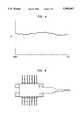
- FIG. 1 illustrates a prior art laser package employing a resistive impedance matching
- FIG. 2 shows the laser package according to the present invention
- FIG. 3 shows graphs of the tilt circuit frequency response and input return loss between 100 MHz to 1 GHz (the tilt circuits input return loss);
- FIG. 4 shows the frequency response of the laser package of FIG. 2.
- FIG. 5 shows an Integrated Laser Module package suitable for housing the components as shown in FIG. 2.
- the present invention is directed to a laser package which houses a semiconductor laser, preferably an analog semiconductor laser which operates from 50 MHz to 1 GHz or higher.
- the package is preferably dimensioned at around one inch by 0.6 inches by 0.4 inches, having 14 dual-side pinouts with seven pins on each side having 0.1 inch centers.
- the package is also preferably hermetically sealed. This type of package is commonly known to one skilled in the art as the 14 pin butterfly ILM package.
- An ILM package suitable for the device according to the present invention is shown in FIG. 5. The components enclosed therein are shown in FIG. 2.
- the laser package according to the present invention takes advantage of the analog lasers being a current driven device and the transformer being constant power devices. Given the modulation current expressed as: ##EQU1##
- I(t) is the modulation current as a function of time
- I 0 is the bias current
- I th is the threshold current of the laser
- m i is the modulation index
- f i is the modulation frequency
- ⁇ i is the phase of the modulation signal.
- the current of the transformer being a constant power device, can be expressed as:
- Is is the current in the transformer secondary
- Zs is the impedance of the secondary winding
- Ip and Zp are the primary current and impedance, respectively.
- Is is the same as the modulation current I(t). Also, it can be seen from the above equations that the modulation current Im or Is is modified by the square root of the ratio of the secondary to primary impedances of the transformer. Therefore, by appropriate selection of Zs and Zp, it is possible to increase or step up the modulation current which passes through the laser for a fixed input (primary) current. Alternatively, it is possible to provide a fixed modulation current to the laser with a reduced input current.
- the laser package 10 includes semiconductor laser LD which is connected to interface 20 which is integrally connected within the laser package 10.
- the interface circuit 20 has an input RF impedance at around 75 ohms and an output RF impedance at around 25 ohms; it passes a DC bias current while stepping up the modulation current.
- the interface circuit includes a "tilt" circuit which serves as an equalization circuit for compensating the negative sloping effects of transformer T1 at higher frequencies. It can be seen that with the placement of the interface circuit 20, including the transformer T1 inside the laser package 10, the line length of the connection between the transformer T1 and the semiconductor laser LD is minimal and the problems associated with stray capacitive effects at high frequencies are virtually eliminated.
- the laser source drive circuit (not shown) produces a DC bias current Idc and a modulation current Im through coil Ldc and capacitor Cc, respectively, Idc and Im are coupled in a bias tee format and are input to the laser package 10 through a single input lead 15.
- an RF choke of around 500 nanohenries passes the DC bias current Idc to laser LD while blocking the modulation current Im.
- the modulation current Im passes capacitors C1, through transformer T1, capacitor C2, and through tilt circuit (Rt and Ct) to the laser LD.
- C1 and C2 are preferably 0.1 microfarad capacitors which pass RF modulation signals and block any DC component of the modulation signal.
- Transformer T1 has a primary winding P1 having an RF impedance of around 75 ohms and a secondary winding S1 having an RF impedance at around 25 ohms. With these impedances and applying equation 3 above, it can be shown that the laser modulation current is stepped up or increased by about 4.77 dB. With the secondary winding of T1 at 25 ohms and the laser LD at 5 ohms, the resistor Rt is chosen to be 20 ohms to match the impedances.
- Interface circuit 20 includes a "tilt" circuit which is formed by resistor Rt and capacitor Ct, with Ct being a 10 picofrarad capacitor.
- the tilt circuit has positive sloping characteristics which interacts with the modulation signal output from the secondary S1 of the transformer T1 to compensate the negative sloping effects of the transformer laser package, enabling operation of the laser package to one GHz or higher.
- the circuitry of the interface 20 as configured enables the integration of the interface 20 into the laser package 10 without requiting a change in the pinout of the butterfly package 10.
- FIG. 3 shows the effect of the tilt circuit on the input signal at frequencies from 100 MHz to 1 GHz.
- Graph A shows the tilt circuit's input return loss and graph B shows the frequency response of the tilt circuit.
- the tilt circuit improves the circuit amplitude by 2.5 dB at frequencies up to 1 GHz.
- FIG. 4 shows the frequency response of the laser package 10 having the interface 20 as shown in FIG. 2. As shown, the frequency response is relatively flat throughout the operation range of 100 MHz to 1 GHz.
Landscapes
- Physics & Mathematics (AREA)
- Condensed Matter Physics & Semiconductors (AREA)
- General Physics & Mathematics (AREA)
- Electromagnetism (AREA)
- Optics & Photonics (AREA)
- Semiconductor Lasers (AREA)
Abstract
Description
Is.sup.2 Zs=Ip.sup.2 Zp (2)
Claims (11)
Priority Applications (4)
| Application Number | Priority Date | Filing Date | Title |
|---|---|---|---|
| US08/304,997 US5500867A (en) | 1994-09-13 | 1994-09-13 | Laser package having an impedance matching transformer |
| DE69523849T DE69523849T2 (en) | 1994-09-13 | 1995-09-06 | Laser module with impedance matching transformer |
| EP95306221A EP0702436B1 (en) | 1994-09-13 | 1995-09-06 | Laser package having an impedance matching transformer |
| JP7234827A JPH0888437A (en) | 1994-09-13 | 1995-09-13 | Laser package with impedance matching transformer |
Applications Claiming Priority (1)
| Application Number | Priority Date | Filing Date | Title |
|---|---|---|---|
| US08/304,997 US5500867A (en) | 1994-09-13 | 1994-09-13 | Laser package having an impedance matching transformer |
Publications (1)
| Publication Number | Publication Date |
|---|---|
| US5500867A true US5500867A (en) | 1996-03-19 |
Family
ID=23178857
Family Applications (1)
| Application Number | Title | Priority Date | Filing Date |
|---|---|---|---|
| US08/304,997 Expired - Lifetime US5500867A (en) | 1994-09-13 | 1994-09-13 | Laser package having an impedance matching transformer |
Country Status (4)
| Country | Link |
|---|---|
| US (1) | US5500867A (en) |
| EP (1) | EP0702436B1 (en) |
| JP (1) | JPH0888437A (en) |
| DE (1) | DE69523849T2 (en) |
Cited By (21)
| Publication number | Priority date | Publication date | Assignee | Title |
|---|---|---|---|---|
| US5748657A (en) * | 1996-08-26 | 1998-05-05 | The United States Of America As Represented By The Secretary Of The Air Force | High efficiency constant current laser driver |
| US5757027A (en) * | 1995-11-06 | 1998-05-26 | International Business Machines Corporation | Semiconductor wafer testing method and apparatus |
| US5982793A (en) * | 1996-05-20 | 1999-11-09 | Matsushita Electric Industrial Co., Ltd. | Semiconductor laser module with internal matching circuit |
| US20020031297A1 (en) * | 1998-06-24 | 2002-03-14 | The Trustees Of Princeton University | Twin waveguide based design for photonic integrated circuits |
| US20020141465A1 (en) * | 2001-03-21 | 2002-10-03 | Shigehiro Yamada | Semiconductor laser device and method for producing the same |
| US20030035451A1 (en) * | 2001-08-09 | 2003-02-20 | Masaaki Ishida | Laser driver circuit |
| US20040076434A1 (en) * | 2002-09-27 | 2004-04-22 | Whittaker G. Allan | Optical distribution network for RF and other analog signals |
| US20050213973A1 (en) * | 2003-03-31 | 2005-09-29 | Rohrer Thomas J | Optical network interface systems and devices |
| US20060013273A1 (en) * | 2004-04-14 | 2006-01-19 | The Trustees Of Princeton University | Monolithic wavelength stabilized asymmetric laser |
| US20070110357A1 (en) * | 2005-11-15 | 2007-05-17 | Forrest Stephen R | Integrated photonic amplifier and detector |
| US7283480B1 (en) | 2002-11-12 | 2007-10-16 | Lockheed Martin Corporation | Network system health monitoring using cantor set signals |
| US7333689B2 (en) | 2005-09-30 | 2008-02-19 | The Trustees Of Princeton University | Photonic integrated devices having reduced absorption loss |
| US7349629B1 (en) | 2002-11-26 | 2008-03-25 | Lockheed Martin Corporation | Methods and systems for creating a digital interconnect fabric |
| USRE40425E1 (en) | 2002-09-27 | 2008-07-08 | Lockheed Martin Corporation | Optical interface devices having balanced amplification |
| US7424228B1 (en) * | 2003-03-31 | 2008-09-09 | Lockheed Martin Corporation | High dynamic range radio frequency to optical link |
| US20080219662A1 (en) * | 2006-10-26 | 2008-09-11 | The Trustees Of Princeton University | Monolithically Integrated Reconfigurable Optical Add-Drop Multiplexer |
| CN100423389C (en) * | 2005-02-04 | 2008-10-01 | 三菱电机株式会社 | Optical module |
| US7440699B1 (en) | 2004-06-28 | 2008-10-21 | Lockheed Martin Corporation | Systems, devices and methods for transmitting and receiving signals on an optical network |
| US20090052485A1 (en) * | 2005-06-01 | 2009-02-26 | Canon Kabushiki Kaisha | Laser driving circuit |
| USRE41247E1 (en) | 1997-04-01 | 2010-04-20 | Lockheed Martin Corporation | Optical transport system |
| CN108683065A (en) * | 2018-03-29 | 2018-10-19 | 昂纳信息技术(深圳)有限公司 | A kind of laser aid |
Families Citing this family (3)
| Publication number | Priority date | Publication date | Assignee | Title |
|---|---|---|---|---|
| WO2006095332A1 (en) * | 2005-03-06 | 2006-09-14 | Mempile Ltd. | A method of driving a laser diode |
| DE102008022253A1 (en) | 2008-05-06 | 2009-11-12 | Miva Technologies Gmbh | High-resolution photoplotting method and arrangement for the high-resolution recording of a computer-stored raster image on a planar photosensitive recording medium |
| WO2021003359A1 (en) * | 2019-07-02 | 2021-01-07 | Omron Corporation | Electronics driver for pulsed discharge |
Citations (5)
| Publication number | Priority date | Publication date | Assignee | Title |
|---|---|---|---|---|
| US4379273A (en) * | 1981-06-25 | 1983-04-05 | Mcdonnell Douglas Corporation | Pulse transformer laser diode package |
| US4485361A (en) * | 1982-12-23 | 1984-11-27 | The United States Of America As Represented By The Secretary Of The Air Force | Pulse transformer package for impedance matching a laser diode to a transmission line |
| US5132639A (en) * | 1989-09-07 | 1992-07-21 | Ortel Corporation | Predistorter for linearization of electronic and optical signals |
| US5216393A (en) * | 1991-02-02 | 1993-06-01 | Robert Bosch Gmbh | High frequency broadband tv signal transformer, especially for 47-860 mhz band |
| US5361156A (en) * | 1991-12-09 | 1994-11-01 | Scientific-Atlanta, Inc. | Method and apparatus for predistortion |
Family Cites Families (3)
| Publication number | Priority date | Publication date | Assignee | Title |
|---|---|---|---|---|
| GB8520923D0 (en) * | 1985-08-21 | 1985-09-25 | Gen Electric | Amplitude modulating output of laser diode |
| NL8901523A (en) * | 1989-06-16 | 1991-01-16 | Philips Nv | LASER DIODE MODULE. |
| US5471492A (en) * | 1992-12-01 | 1995-11-28 | Scientific Atlanta, Inc. | Broadband matching network |
-
1994
- 1994-09-13 US US08/304,997 patent/US5500867A/en not_active Expired - Lifetime
-
1995
- 1995-09-06 EP EP95306221A patent/EP0702436B1/en not_active Expired - Lifetime
- 1995-09-06 DE DE69523849T patent/DE69523849T2/en not_active Expired - Fee Related
- 1995-09-13 JP JP7234827A patent/JPH0888437A/en active Pending
Patent Citations (5)
| Publication number | Priority date | Publication date | Assignee | Title |
|---|---|---|---|---|
| US4379273A (en) * | 1981-06-25 | 1983-04-05 | Mcdonnell Douglas Corporation | Pulse transformer laser diode package |
| US4485361A (en) * | 1982-12-23 | 1984-11-27 | The United States Of America As Represented By The Secretary Of The Air Force | Pulse transformer package for impedance matching a laser diode to a transmission line |
| US5132639A (en) * | 1989-09-07 | 1992-07-21 | Ortel Corporation | Predistorter for linearization of electronic and optical signals |
| US5216393A (en) * | 1991-02-02 | 1993-06-01 | Robert Bosch Gmbh | High frequency broadband tv signal transformer, especially for 47-860 mhz band |
| US5361156A (en) * | 1991-12-09 | 1994-11-01 | Scientific-Atlanta, Inc. | Method and apparatus for predistortion |
Cited By (32)
| Publication number | Priority date | Publication date | Assignee | Title |
|---|---|---|---|---|
| US5757027A (en) * | 1995-11-06 | 1998-05-26 | International Business Machines Corporation | Semiconductor wafer testing method and apparatus |
| US6273400B1 (en) * | 1995-11-06 | 2001-08-14 | International Business Machines Corporation | Semiconductor wafer testing structure |
| US5982793A (en) * | 1996-05-20 | 1999-11-09 | Matsushita Electric Industrial Co., Ltd. | Semiconductor laser module with internal matching circuit |
| US5748657A (en) * | 1996-08-26 | 1998-05-05 | The United States Of America As Represented By The Secretary Of The Air Force | High efficiency constant current laser driver |
| USRE41247E1 (en) | 1997-04-01 | 2010-04-20 | Lockheed Martin Corporation | Optical transport system |
| US20020031297A1 (en) * | 1998-06-24 | 2002-03-14 | The Trustees Of Princeton University | Twin waveguide based design for photonic integrated circuits |
| US7327910B2 (en) | 1998-06-24 | 2008-02-05 | The Trustees Of Princeton University | Twin waveguide based design for photonic integrated circuits |
| US7302124B2 (en) | 1998-06-24 | 2007-11-27 | The Trustees Of Princeton University | Twin waveguide based design for photonic integrated circuits |
| US6847665B2 (en) * | 2001-03-21 | 2005-01-25 | Sharp Kabushiki Kaisha | Semiconductor laser device and method for producing the same |
| US20020141465A1 (en) * | 2001-03-21 | 2002-10-03 | Shigehiro Yamada | Semiconductor laser device and method for producing the same |
| US6917639B2 (en) * | 2001-08-09 | 2005-07-12 | Ricoh Company, Ltd. | Laser driver circuit |
| US20030035451A1 (en) * | 2001-08-09 | 2003-02-20 | Masaaki Ishida | Laser driver circuit |
| US20040076434A1 (en) * | 2002-09-27 | 2004-04-22 | Whittaker G. Allan | Optical distribution network for RF and other analog signals |
| USRE40425E1 (en) | 2002-09-27 | 2008-07-08 | Lockheed Martin Corporation | Optical interface devices having balanced amplification |
| US7283480B1 (en) | 2002-11-12 | 2007-10-16 | Lockheed Martin Corporation | Network system health monitoring using cantor set signals |
| US7349629B1 (en) | 2002-11-26 | 2008-03-25 | Lockheed Martin Corporation | Methods and systems for creating a digital interconnect fabric |
| US7424228B1 (en) * | 2003-03-31 | 2008-09-09 | Lockheed Martin Corporation | High dynamic range radio frequency to optical link |
| US20050213973A1 (en) * | 2003-03-31 | 2005-09-29 | Rohrer Thomas J | Optical network interface systems and devices |
| US7570887B2 (en) | 2003-03-31 | 2009-08-04 | Lockheed Martin Corporation | Optical network interface systems and devices |
| US20060013273A1 (en) * | 2004-04-14 | 2006-01-19 | The Trustees Of Princeton University | Monolithic wavelength stabilized asymmetric laser |
| US7230963B2 (en) | 2004-04-14 | 2007-06-12 | The Trustees Of Princeton University | Monolithic wavelength stabilized asymmetric laser |
| US7440699B1 (en) | 2004-06-28 | 2008-10-21 | Lockheed Martin Corporation | Systems, devices and methods for transmitting and receiving signals on an optical network |
| CN100423389C (en) * | 2005-02-04 | 2008-10-01 | 三菱电机株式会社 | Optical module |
| US20090052485A1 (en) * | 2005-06-01 | 2009-02-26 | Canon Kabushiki Kaisha | Laser driving circuit |
| US7697582B2 (en) * | 2005-06-01 | 2010-04-13 | Canon Kabushiki Kaisha | Laser driving circuit |
| US7333689B2 (en) | 2005-09-30 | 2008-02-19 | The Trustees Of Princeton University | Photonic integrated devices having reduced absorption loss |
| US20070110357A1 (en) * | 2005-11-15 | 2007-05-17 | Forrest Stephen R | Integrated photonic amplifier and detector |
| US7343061B2 (en) | 2005-11-15 | 2008-03-11 | The Trustees Of Princeton University | Integrated photonic amplifier and detector |
| US20080219662A1 (en) * | 2006-10-26 | 2008-09-11 | The Trustees Of Princeton University | Monolithically Integrated Reconfigurable Optical Add-Drop Multiplexer |
| US7826693B2 (en) | 2006-10-26 | 2010-11-02 | The Trustees Of Princeton University | Monolithically integrated reconfigurable optical add-drop multiplexer |
| CN108683065A (en) * | 2018-03-29 | 2018-10-19 | 昂纳信息技术(深圳)有限公司 | A kind of laser aid |
| CN108683065B (en) * | 2018-03-29 | 2024-01-19 | 昂纳科技(深圳)集团股份有限公司 | Laser device |
Also Published As
| Publication number | Publication date |
|---|---|
| DE69523849T2 (en) | 2002-06-27 |
| DE69523849D1 (en) | 2001-12-20 |
| EP0702436A2 (en) | 1996-03-20 |
| JPH0888437A (en) | 1996-04-02 |
| EP0702436B1 (en) | 2001-11-14 |
| EP0702436A3 (en) | 1996-05-29 |
Similar Documents
| Publication | Publication Date | Title |
|---|---|---|
| US5500867A (en) | Laser package having an impedance matching transformer | |
| US6437899B1 (en) | Opto-electric conversion semiconductor device | |
| US5706303A (en) | Laser diode coupling and bias circuit and method | |
| US7030477B2 (en) | Optical semiconductor device | |
| US7035302B2 (en) | Optical transmission module | |
| US6522083B1 (en) | Driver circuitry with tuned output impedance | |
| US5602672A (en) | Light modulator module and method for fabricating light modulator module | |
| US20040247004A1 (en) | Optical element module package and method for manufacturing the same | |
| US6823145B1 (en) | Optical transmitter module | |
| EP0221710A2 (en) | Apparatus for controlling the power of a laser | |
| JP2002324866A (en) | Electronic package | |
| US5471492A (en) | Broadband matching network | |
| JPS6333882A (en) | Drive circuit for laser diode | |
| KR0181896B1 (en) | Wide-band device of fast optical module | |
| US5732097A (en) | Modulating circuit for semiconductor optical modulator | |
| US5995261A (en) | Capacitors on dielectric feedthrus for metal packages | |
| JPH07143182A (en) | Optical transmission device | |
| US5793516A (en) | Optical modulator circuit | |
| US6788447B2 (en) | Off-chip matching circuit for electroabsorption optical modulator | |
| US7391797B2 (en) | Integrated circuit for controlling a laser diode | |
| US5444727A (en) | Laser head | |
| JP2002076508A (en) | Method and device for decreasing electric crosstalk and wavelength chirp inside distributed bragg's reflector laser | |
| US6850546B2 (en) | Driver circuit | |
| US20230244094A1 (en) | Optical communication device | |
| JP2002237644A (en) | Optical transmitter |
Legal Events
| Date | Code | Title | Description |
|---|---|---|---|
| AS | Assignment |
Owner name: AT&T CORP., NEW YORK Free format text: ASSIGNMENT OF ASSIGNORS INTEREST;ASSIGNOR:KRASULICK, S.B. 1;REEL/FRAME:007144/0850 Effective date: 19940906 |
|
| STCF | Information on status: patent grant |
Free format text: PATENTED CASE |
|
| FEPP | Fee payment procedure |
Free format text: PAYOR NUMBER ASSIGNED (ORIGINAL EVENT CODE: ASPN); ENTITY STATUS OF PATENT OWNER: LARGE ENTITY |
|
| FPAY | Fee payment |
Year of fee payment: 4 |
|
| FEPP | Fee payment procedure |
Free format text: PAYOR NUMBER ASSIGNED (ORIGINAL EVENT CODE: ASPN); ENTITY STATUS OF PATENT OWNER: LARGE ENTITY Free format text: PAYER NUMBER DE-ASSIGNED (ORIGINAL EVENT CODE: RMPN); ENTITY STATUS OF PATENT OWNER: LARGE ENTITY |
|
| FPAY | Fee payment |
Year of fee payment: 8 |
|
| FPAY | Fee payment |
Year of fee payment: 12 |
|
| AS | Assignment |
Owner name: DEUTSCHE BANK AG NEW YORK BRANCH, AS COLLATERAL AG Free format text: PATENT SECURITY AGREEMENT;ASSIGNORS:LSI CORPORATION;AGERE SYSTEMS LLC;REEL/FRAME:032856/0031 Effective date: 20140506 |
|
| AS | Assignment |
Owner name: AVAGO TECHNOLOGIES GENERAL IP (SINGAPORE) PTE. LTD Free format text: ASSIGNMENT OF ASSIGNORS INTEREST;ASSIGNOR:AGERE SYSTEMS LLC;REEL/FRAME:035365/0634 Effective date: 20140804 |
|
| AS | Assignment |
Owner name: AGERE SYSTEMS LLC, PENNSYLVANIA Free format text: TERMINATION AND RELEASE OF SECURITY INTEREST IN PATENT RIGHTS (RELEASES RF 032856-0031);ASSIGNOR:DEUTSCHE BANK AG NEW YORK BRANCH, AS COLLATERAL AGENT;REEL/FRAME:037684/0039 Effective date: 20160201 Owner name: LSI CORPORATION, CALIFORNIA Free format text: TERMINATION AND RELEASE OF SECURITY INTEREST IN PATENT RIGHTS (RELEASES RF 032856-0031);ASSIGNOR:DEUTSCHE BANK AG NEW YORK BRANCH, AS COLLATERAL AGENT;REEL/FRAME:037684/0039 Effective date: 20160201 |