US5278404A - Optical sub-system utilizing an embedded micro-controller - Google Patents
Optical sub-system utilizing an embedded micro-controller Download PDFInfo
- Publication number
- US5278404A US5278404A US07/916,934 US91693492A US5278404A US 5278404 A US5278404 A US 5278404A US 91693492 A US91693492 A US 91693492A US 5278404 A US5278404 A US 5278404A
- Authority
- US
- United States
- Prior art keywords
- sub
- optical
- controller
- micro
- operating parameters
- Prior art date
- Legal status (The legal status is an assumption and is not a legal conclusion. Google has not performed a legal analysis and makes no representation as to the accuracy of the status listed.)
- Expired - Lifetime
Links
Images


Classifications
-
- H—ELECTRICITY
- H04—ELECTRIC COMMUNICATION TECHNIQUE
- H04B—TRANSMISSION
- H04B10/00—Transmission systems employing electromagnetic waves other than radio-waves, e.g. infrared, visible or ultraviolet light, or employing corpuscular radiation, e.g. quantum communication
- H04B10/07—Arrangements for monitoring or testing transmission systems; Arrangements for fault measurement of transmission systems
-
- H—ELECTRICITY
- H04—ELECTRIC COMMUNICATION TECHNIQUE
- H04B—TRANSMISSION
- H04B10/00—Transmission systems employing electromagnetic waves other than radio-waves, e.g. infrared, visible or ultraviolet light, or employing corpuscular radiation, e.g. quantum communication
- H04B10/29—Repeaters
- H04B10/291—Repeaters in which processing or amplification is carried out without conversion of the main signal from optical form
- H04B10/293—Signal power control
- H04B10/294—Signal power control in a multiwavelength system, e.g. gain equalisation
- H04B10/2942—Signal power control in a multiwavelength system, e.g. gain equalisation using automatic gain control [AGC]
-
- H—ELECTRICITY
- H01—ELECTRIC ELEMENTS
- H01S—DEVICES USING THE PROCESS OF LIGHT AMPLIFICATION BY STIMULATED EMISSION OF RADIATION [LASER] TO AMPLIFY OR GENERATE LIGHT; DEVICES USING STIMULATED EMISSION OF ELECTROMAGNETIC RADIATION IN WAVE RANGES OTHER THAN OPTICAL
- H01S5/00—Semiconductor lasers
- H01S5/04—Processes or apparatus for excitation, e.g. pumping, e.g. by electron beams
- H01S5/042—Electrical excitation ; Circuits therefor
-
- H—ELECTRICITY
- H04—ELECTRIC COMMUNICATION TECHNIQUE
- H04B—TRANSMISSION
- H04B10/00—Transmission systems employing electromagnetic waves other than radio-waves, e.g. infrared, visible or ultraviolet light, or employing corpuscular radiation, e.g. quantum communication
- H04B10/29—Repeaters
-
- H—ELECTRICITY
- H04—ELECTRIC COMMUNICATION TECHNIQUE
- H04B—TRANSMISSION
- H04B10/00—Transmission systems employing electromagnetic waves other than radio-waves, e.g. infrared, visible or ultraviolet light, or employing corpuscular radiation, e.g. quantum communication
- H04B10/50—Transmitters
-
- H—ELECTRICITY
- H01—ELECTRIC ELEMENTS
- H01S—DEVICES USING THE PROCESS OF LIGHT AMPLIFICATION BY STIMULATED EMISSION OF RADIATION [LASER] TO AMPLIFY OR GENERATE LIGHT; DEVICES USING STIMULATED EMISSION OF ELECTROMAGNETIC RADIATION IN WAVE RANGES OTHER THAN OPTICAL
- H01S5/00—Semiconductor lasers
- H01S5/06—Arrangements for controlling the laser output parameters, e.g. by operating on the active medium
- H01S5/068—Stabilisation of laser output parameters
- H01S5/06825—Protecting the laser, e.g. during switch-on/off, detection of malfunctioning or degradation
Definitions
- the present invention relates to performance optimization of an optical sub-system and, more particularly to utilizing an embedded micro-controller to provide the optimization.
- Analog feedback circuitry is often utilized to provide a moderate degree of control in some situations as, for example, controlling the bias voltage applied to a laser transmitter, the transimpedance gain of a receiver pre-amplifier, the gain of an optical amplifier, or various combinations of the above.
- U.S. Pat. No. 4,924,191 issued to L. A. Erb et al. on May 8, 1990 discusses a solution to the various problems associated with utilizing analog feedback circuits (in this case, however, not for an optical system, but an electrical power amplifier).
- the operating bias point for an electrical power amplifier is stored in a computer memory. During frequent test intervals (when an incoming signal is interrupted), a test signal is passed through the power amplifier and a test bias point is measured. The test bias is then compared (by the computer) with the operating bias stored in memory. If they differ, the memory is updated to load the test bias value and the operation mode of the amplifier is re-started, where the updated value will be used to bias the amplifier until the next test period initiated.
- the computer alternatively, may be programmed by the user to bypass the test mode and continuously run using a user-supplied bias voltage value.
- the present invention relates to performance optimization of an optical sub-system and, more particularly, to utilizing an embedded micro-controller to provide the desired optimization.
- an optical sub-system arrangement during manufacture, is subjected to a full range of environmental changes (e.g., minimum to maximum ambient temperature, input signal conditions, device(s) aging, etc.) and the required operating parameters (e.g., bias voltages) associated with optimum performance (e.g., minimum bit error rate) are recorded at a number of points chosen along the range of environmental changes and stored in a micro-controller embedded within the optical sub-system.
- environmental changes e.g., minimum to maximum ambient temperature, input signal conditions, device(s) aging, etc.
- the required operating parameters e.g., bias voltages
- optimum performance e.g., minimum bit error rate
- the micro-controller may be configured to accept program changes from the user/customer so as to adapt the performance of the sub-system for particular conditions (e.g., non-optimum performance for supplying additional power or increased bit error rate constraints) which then override the values stored in memory.
- each sub-system may be individually tuned such that the embedded micro-controller is tailored to optimize the sub-system performance. Such optimization may be beyond that which had been possible with analog feedback circuitry, thus increasing the manufacturing yield of the sub-system.
- Another advantage of an optical sub-system formed in accordance with the present invention is that the embedded micro-controller may be configured to maintain in memory all changes in operating parameters over the life of the sub-system. These changes are often of interest to the system design engineers with respect to future system designs.
- FIG. 1 illustrates, in block diagram form, an exemplary factory set-up for performing the initialization of an embedded micro-controller
- FIG. 2 illustrates an exemplary optical regenerator arrangement utilizing an embedded micro-controller to provide performance optimization in accordance with the teachings of the present invention
- FIG. 3 illustrates an alternative application of micro-controller performance optimization, in particular, as utilized within a doped fiber optical amplifier arrangement.
- FIG. 1 illustrates, in block diagram form, an exemplary manufacturing line configuration 10 for initially programming the micro-controller portion of an optical sub-system in accordance with the teachings of the present invention.
- a selected optical sub-system before field deployment, is subjected to the full range of environmental changes expected to be present over the lifetime of the sub-system.
- the most important environmental changes are ambient temperature, input signal power levels, and the aging of individual device(s) within the sub-system.
- Configuration 10 is a useful arrangement for initially subjecting the optical sub-system to a predetermined set of environmental changes and recording the changes in sub-system parameters as a function of these environmental changes.
- the embedded micro-controller is utilized to modify the performance of the sub-system as the actual environment changes.
- an exemplary sub-system 12 for example, a laser transmitter, APD receiver, optical amplifier or regenerator
- an embedded micro-controller 14 is placed in an oven 16.
- a test set computer 18 is provided in configuration 10 and is initially programmed to include the complete range of testing desired for the specific type of sub-system being studied. Test set computer 18, as shown in FIG. 1, then communicates the test program to embedded micro-controller 14. Test set computer 18 is also directly coupled to the controls of oven 16, as well as various other external testing devices (e.g., input signal attenuators). For example, test set computer 18 may also be coupled to a bit error rate (BER) test monitor 20.
- BER bit error rate
- BER test monitor 20 is used, at each specific temperature under study, to locate the minimum bit error rate for an exemplary (worst-case) test signal. Additional test equipment 22 is utilized to vary the associated operating parameters of sub-system 12 (e.g., bias voltages, device temperatures, transimpedance gain) until the minimum BER is achieved. Once determined, the operating parameters associated with optimum performance at a specific temperature (and input signal level, perhaps) are transmitted back through test set computer 18 to a ROM programmer 24. Included within programmer 24 is a memory element 26, such as a ROM chip, which is programmed to store the data. ROM 26 will then be inserted in micro-controller 14 when the testing is completed.
- ROM programmer 24 included within programmer 24 is a memory element 26, such as a ROM chip, which is programmed to store the data. ROM 26 will then be inserted in micro-controller 14 when the testing is completed.
- the data generated by the testing process and transmitted back to test set computer 18 may also be displayed in any desired form (e.g., visual display, plot, graph, table, etc.) within a data presentation unit 28, as shown in phantom in FIG. 1.
- ROM chip 26 is inserted within embedded micro-controller 14 to be packaged as a finished optical sub-system.
- FIG. 2 illustrates an exemplary regenerator arrangement 30 including an embedded micro-controller 32 in accordance with the teachings of the present invention.
- regenerator 30 is used in an optical communication system to restore (or "regenerate") an optical signal which must travel an extensive distance between transmitter and receiver.
- a regenerator functions to receive the optical signal propagating along the fiber, convert the optical signal into an electrical representation, re-create the electrical signal so as to include sharp transitions between logic "1"'s and logic "0"'s, and finally, re-convert the electrical signal into an optical signal to be re-coupled into the fiber. This process is shown in some detail in FIG. 2.
- An incoming optical data signal I is applied as an input to a receiver 34 which functions to convert the optical signal into the electrical representation.
- the electrical signal E is applied as an input to a decision circuit 36 which determines the logic value of each data bit as it passes through the circuit.
- the two outputs from decision circuit 36 are thus labeled Data and Data.
- the clock signal is also extracted from the electrical signal E.
- Regenerator 30 of FIG. 2 performs clock recovery utilizing an exclusive-OR gate 38, SAW filter 40 and phase shifter 42, positioned in series as shown in FIG. 2.
- the output from phase shifter 42, the recovered clock signal Clk is fed back as an input to decision circuit 36 to provide the correct timing of the data output signal.
- Clock signal Clk also appears as a separate output signal, as shown in FIG. 2, and may further be used to generate a signal indicating loss of transmission, referred to in FIG. 2 as an "Alarm" signal.
- a threshold detector 44 may be utilized to compare clock signal Clk to a reference voltage to generate the alarm
- embedded micro-controller 32 may be utilized to monitor a number of different operating parameters of regenerator 30 and provide adjustments, over time, to these parameters so as to continuously optimize the performance of regenerator 30 with respect to changes in the environment (e.g., temperature, device(s) aging, input signal level, power supply variations). Examples of various ones of these parameters will be now be discussed in detail below. It is to be understood, however, that these parameters are exemplary only, and any parameter (and any combination thereof) which may be measured and utilized to provide performance optimization in accordance with the teachings of the present invention. Referring to receiver 34 of FIG.
- the ambient temperature T and photocurrent I R of receiver 32 may be transmitted as operating parameters to micro-controller 32 and utilized by ROM 46 (programmed as discussed above) to determine the optimum feedback voltage (V fb ) and photodetector bias voltage (V APD ) within receiver 34.
- V fb feedback voltage
- V APD photodetector bias voltage
- regenerator 30 is tested under various operating conditions and the parameters (such as feedback voltage and photodetector bias voltage) are measured to determine optimum values for various conditions.
- the embedded micro-controller contains, within its memory, the optimum values associated with these conditions. Therefore, by continuously adjusting (as a function of temperature, for example) the reference voltages applied to the receiver 34, its performance can be optimized. As shown in FIG.
- V fb and V APD are but one pair of outputs from micro-controller 32.
- the threshold voltages V Data and V Clk used to control the outputs from decision circuit 36 are also determined by micro-controller 32, since these voltages may also shift as a function of temperature.
- the reference voltage for alarm unit 44, denoted V alm .ref may also be set, as shown by micro-controller 32, with the actual power level of the clock signal, denoted V alm in FIG. 2, being sent back as data to micro-controller 32.
- a duty cycle detector 48 may be inserted in the clock output line to determine average DC value of the signal, where the DC voltage, denoted V DC in FIG. 2, may also be transmitted as data back to micro-controller 32.
- an additional feature of the present invention may include the ability to override the operation of micro-controller 32 after deployment such that predetermined values for selected operating parameters may be fixed to provide desired operating levels (i.e., maximize V APD to insure maximum sensitivity of receiver 34).
- a terminal 50 may be coupled to micro-controller 32 and used to disable ROM 46 so as to freeze or modify any of the various outputs from micro-controller 32.
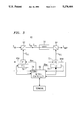
- FIG. 3 illustrates an alternative optical sub-system utilizing an embedded micro-controller to optimize performance in accordance with the teachings of the present invention.
- FIG. 3 contains a simplified diagram of an optical fiber amplifier 60.
- an input optical data signal I IN and optical pump signal I P are applied as simultaneous inputs to a rare earth-doped optical fiber.
- the optical input signal I IN and a first pump signal I P1 are coupled through a first wavelength multiplexer 62 into a section 64 of doped fiber.
- a second pump signal I P2 may be coupled by a second multiplexer 66 to the opposite end of doped fiber 64.
- the presence of the pump signal(s) results in providing gain to the optical data signal.
- the output from amplifier 60 will be an amplified version, I AMP of the input signal.
- pump laser sources may be subject to aging, which may lower the pump laser's available output power, or worse, cause the wavelength of the pump laser to drift.
- the pump wavelength be maintained at a predetermined value, since the amount of gain is a result of Raman mixing at that wavelength. Therefore, in accordance with the teachings of the present invention, a micro-controller 68 is embedded within amplifier 60 and utilized to monitor and continuously optimize the performance of the pump lasers. It is to be noted that although only two such pumps lasers are shown, a fiber amplifier may use a larger number of such pumps and the teachings of the present invention remain applicable.
- the micro-controller portion 68 of optical amplifier 60 is first initially programmed, using an arrangement such as manufacturing line configuration 10 of FIG. 1.
- test set computer 18 is utilized to vary the operating parameters associated with pump sources 70 and 72 as a function of changing environmental conditions (such as ambient temperature).
- a memory element 74 such as a ROM chip, within programmer 24 (see FIG. 1) is thus programmed to store the desired operating parameter values and subsequently inserted in micro-controller 68.
- the light output (L) as a function of input bias current (I bias ) for pump sources 70 and 72 may be determined at each data point and the optimum bias current for maintaining sufficient power at a fixed wavelength is recorded and stored in ROM 74.
- the BER test may be replaced by an L-I test.
- the electrical signal generated by each backface monitor BFM (not shown) associated with sources 70 and 72 are directed as inputs to micro-controller 68, which uses this information to control, in this case the bias current applied to each pump.
- a pair of thermo-electric coolers (TECs) 76,78 is associated with sources 70 and 72, respectively, utilized to adjust the local temperature of the associated laser source so as to maintain maximum output power.
- micro-controller 68 may also be coupled to an external terminal 80 which is used to override the operation of ROM 74 and provide alternate predetermined operating parameters for use by optical amplifier 60.
- an embedded micro-controller may be utilized with any desired optical sub-system to provide self-tuning and performance optimization as a function of various changes in the environment of the optical sub-system.
- an embedded micro-controller may be utilized with a laser transmitter for the purpose of adjusting, for example, the laser temperature, bias current, and/or modulation current as a function of environmental conditions.
Abstract
Description
Claims (6)
Priority Applications (5)
| Application Number | Priority Date | Filing Date | Title |
|---|---|---|---|
| US07/916,934 US5278404A (en) | 1992-07-20 | 1992-07-20 | Optical sub-system utilizing an embedded micro-controller |
| EP93305290A EP0580317A1 (en) | 1992-07-20 | 1993-07-06 | Optical sub-system utilizing an embedded micro-controller |
| KR1019930013302A KR940003225A (en) | 1992-07-20 | 1993-07-15 | Optical sub-system for generating an optical output signal in response to the optical input signal |
| JP5196683A JPH06209290A (en) | 1992-07-20 | 1993-07-15 | Optical subsystem |
| US08/159,904 US5396059A (en) | 1992-07-20 | 1993-12-01 | Digital processor-controlled arrangement for monitoring and modifying system operating parameters |
Applications Claiming Priority (1)
| Application Number | Priority Date | Filing Date | Title |
|---|---|---|---|
| US07/916,934 US5278404A (en) | 1992-07-20 | 1992-07-20 | Optical sub-system utilizing an embedded micro-controller |
Related Child Applications (1)
| Application Number | Title | Priority Date | Filing Date |
|---|---|---|---|
| US08/159,904 Continuation-In-Part US5396059A (en) | 1992-07-20 | 1993-12-01 | Digital processor-controlled arrangement for monitoring and modifying system operating parameters |
Publications (1)
| Publication Number | Publication Date |
|---|---|
| US5278404A true US5278404A (en) | 1994-01-11 |
Family
ID=25438104
Family Applications (2)
| Application Number | Title | Priority Date | Filing Date |
|---|---|---|---|
| US07/916,934 Expired - Lifetime US5278404A (en) | 1992-07-20 | 1992-07-20 | Optical sub-system utilizing an embedded micro-controller |
| US08/159,904 Expired - Lifetime US5396059A (en) | 1992-07-20 | 1993-12-01 | Digital processor-controlled arrangement for monitoring and modifying system operating parameters |
Family Applications After (1)
| Application Number | Title | Priority Date | Filing Date |
|---|---|---|---|
| US08/159,904 Expired - Lifetime US5396059A (en) | 1992-07-20 | 1993-12-01 | Digital processor-controlled arrangement for monitoring and modifying system operating parameters |
Country Status (4)
| Country | Link |
|---|---|
| US (2) | US5278404A (en) |
| EP (1) | EP0580317A1 (en) |
| JP (1) | JPH06209290A (en) |
| KR (1) | KR940003225A (en) |
Cited By (14)
| Publication number | Priority date | Publication date | Assignee | Title |
|---|---|---|---|---|
| US5396059A (en) * | 1992-07-20 | 1995-03-07 | At&T Corp. | Digital processor-controlled arrangement for monitoring and modifying system operating parameters |
| GB2310555A (en) * | 1996-02-26 | 1997-08-27 | Nec Corp | Temperature insensitive regenerative optical receiver |
| US5844928A (en) * | 1996-02-27 | 1998-12-01 | Lucent Technologies, Inc. | Laser driver with temperature sensor on an integrated circuit |
| US6115396A (en) * | 1993-05-05 | 2000-09-05 | Coherent, Inc. | Control system for a laser with multiple solid state rods |
| US6163571A (en) * | 1998-04-24 | 2000-12-19 | Ericsson Inc. | Method for measuring received signal quality in a mobile wireless communication system |
| WO2003069379A2 (en) * | 2002-02-12 | 2003-08-21 | Finisar Corporation | Avalanche photodiode controller circuit for fiber optics transceiver |
| US20030234353A1 (en) * | 2002-05-31 | 2003-12-25 | Jds Uniphase Corporation | Integration of electronic data storage into a telecommunications component |
| US20040079866A1 (en) * | 2002-08-05 | 2004-04-29 | Naoki Nishiyama | Optical receiver and a method for manufacturing the same |
| US20040151173A1 (en) * | 2003-02-05 | 2004-08-05 | Alcatel | Electrical signal regenerator |
| US20040256625A1 (en) * | 2003-06-17 | 2004-12-23 | Catalyst Semiconductor, Inc. | Led driver with integrated bias and dimming control storage |
| US20050231454A1 (en) * | 2002-09-03 | 2005-10-20 | Alben Jonah M | Graphics processor and system with microcontroller for programmable sequencing of power up or power down operations |
| US20090226166A1 (en) * | 2001-02-05 | 2009-09-10 | Aronson Lewis B | Optoelectronic Transceiver with Digital Diagnostics |
| US20100002587A1 (en) * | 2008-07-01 | 2010-01-07 | Gayle Loretta Ray Noble | Diagnostics for Serial Communication Busses |
| US20130051789A1 (en) * | 2011-08-30 | 2013-02-28 | Cyoptics, Inc. | Monitoring Circuitry For Optical Transceivers |
Families Citing this family (76)
| Publication number | Priority date | Publication date | Assignee | Title |
|---|---|---|---|---|
| US5860106A (en) * | 1995-07-13 | 1999-01-12 | Intel Corporation | Method and apparatus for dynamically adjusting power/performance characteristics of a memory subsystem |
| US5812572A (en) * | 1996-07-01 | 1998-09-22 | Pacific Fiberoptics, Inc. | Intelligent fiberoptic transmitters and methods of operating and manufacturing the same |
| US5953690A (en) * | 1996-07-01 | 1999-09-14 | Pacific Fiberoptics, Inc. | Intelligent fiberoptic receivers and method of operating and manufacturing the same |
| JPH11135871A (en) * | 1997-10-28 | 1999-05-21 | Nec Corp | Method for activating laser diode and circuit thereof |
| US6454168B1 (en) | 1998-09-14 | 2002-09-24 | Psc Scanning, Inc. | Correlation and stitching techniques in a bar code scanning system |
| US6494376B1 (en) * | 1998-09-14 | 2002-12-17 | Psc Scanning, Inc. | Compensation for scan line variations in a bar code scanner system |
| US6513714B1 (en) | 1998-09-14 | 2003-02-04 | Psc Scanning, Inc. | Character reconstruction and element level processing in bar code scanning system |
| US6585157B2 (en) | 1998-09-14 | 2003-07-01 | Psc Scanning, Inc. | Symbology determination to aid decoding in a bar code scanning system |
| US6441364B1 (en) | 1999-06-25 | 2002-08-27 | Zvi Regev | Learned behavior optical power source controller |
| US6263136B1 (en) * | 1999-10-29 | 2001-07-17 | Lucent Technologies | Intelligent optical transmitter module |
| US6313459B1 (en) | 2000-05-31 | 2001-11-06 | Nortel Networks Limited | Method for calibrating and operating an uncooled avalanche photodiode optical receiver |
| JP4689008B2 (en) * | 2000-07-04 | 2011-05-25 | 富士通株式会社 | Method and apparatus for waveform shaping of signal light |
| JP3729045B2 (en) * | 2000-08-30 | 2005-12-21 | 日本電気株式会社 | Optical module abnormality detection method and apparatus |
| KR100369658B1 (en) | 2000-09-05 | 2003-01-30 | 삼성전자 주식회사 | Bit rate control device of optical receiver and method thereof |
| US6839364B1 (en) | 2000-09-29 | 2005-01-04 | Triquint Technology Holding Co. | Feedback control loop operating system for tunable source |
| US7181146B1 (en) | 2001-01-17 | 2007-02-20 | Optical Communication Products, Inc. | Self-adjusting data transmitter |
| US7346278B2 (en) * | 2001-02-05 | 2008-03-18 | Finisar Corporation | Analog to digital signal conditioning in optoelectronic transceivers |
| US7149430B2 (en) * | 2001-02-05 | 2006-12-12 | Finsiar Corporation | Optoelectronic transceiver having dual access to onboard diagnostics |
| US20040197101A1 (en) * | 2001-02-05 | 2004-10-07 | Sasser Gary D. | Optical transceiver module with host accessible on-board diagnostics |
| US7302186B2 (en) | 2001-02-05 | 2007-11-27 | Finisar Corporation | Optical transceiver and host adapter with memory mapped monitoring circuitry |
| WO2002089390A1 (en) * | 2001-04-26 | 2002-11-07 | Rohde & Schwarz Gmbh & Co. Kg | Method for testing the error ratio of a device |
| GB2377838A (en) * | 2001-07-21 | 2003-01-22 | Zarlink Semiconductor Ab | Programmable EPROM controller for optical transmitter array |
| US6975642B2 (en) | 2001-09-17 | 2005-12-13 | Finisar Corporation | Optoelectronic device capable of participating in in-band traffic |
| US6862302B2 (en) * | 2002-02-12 | 2005-03-01 | Finisar Corporation | Maintaining desirable performance of optical emitters over temperature variations |
| US7516373B2 (en) * | 2002-05-08 | 2009-04-07 | Rohde & Schwarz Gmbh & Co. Kg | Method for testing the error ratio of a device using a preliminary probability |
| US7486894B2 (en) * | 2002-06-25 | 2009-02-03 | Finisar Corporation | Transceiver module and integrated circuit with dual eye openers |
| US7561855B2 (en) * | 2002-06-25 | 2009-07-14 | Finisar Corporation | Transceiver module and integrated circuit with clock and data recovery clock diplexing |
| US7437079B1 (en) | 2002-06-25 | 2008-10-14 | Finisar Corporation | Automatic selection of data rate for optoelectronic devices |
| US7664401B2 (en) * | 2002-06-25 | 2010-02-16 | Finisar Corporation | Apparatus, system and methods for modifying operating characteristics of optoelectronic devices |
| US7809275B2 (en) * | 2002-06-25 | 2010-10-05 | Finisar Corporation | XFP transceiver with 8.5G CDR bypass |
| US7477847B2 (en) * | 2002-09-13 | 2009-01-13 | Finisar Corporation | Optical and electrical channel feedback in optical transceiver module |
| US7089459B2 (en) * | 2002-09-30 | 2006-08-08 | Intel Corporation | Limit interface for performance management |
| US7136772B2 (en) * | 2002-11-08 | 2006-11-14 | Avago Technologies Fiber Ip (Singapore) Pte. Ltd. | Monitoring system for a communications network |
| US7317743B2 (en) * | 2002-11-08 | 2008-01-08 | Finisar Corporation | Temperature and jitter compensation controller circuit and method for fiber optics device |
| US7230961B2 (en) | 2002-11-08 | 2007-06-12 | Finisar Corporation | Temperature and jitter compensation controller circuit and method for fiber optics device |
| US7426586B2 (en) * | 2003-12-15 | 2008-09-16 | Finisar Corporation | Configurable input/output terminals |
| US7702030B2 (en) * | 2003-12-17 | 2010-04-20 | Mindspeed Technologies, Inc. | Module to module signaling with jitter modulation |
| US20050180711A1 (en) * | 2004-02-13 | 2005-08-18 | Kamath Kishore K. | Dual loop automatic power control of optical transmitters |
| US7630631B2 (en) * | 2004-04-14 | 2009-12-08 | Finisar Corporation | Out-of-band data communication between network transceivers |
| US8639122B2 (en) | 2004-07-02 | 2014-01-28 | Finisar Corporation | Filtering digital diagnostics information in an optical transceiver prior to reporting to host |
| US7447438B2 (en) | 2004-07-02 | 2008-11-04 | Finisar Corporation | Calibration of digital diagnostics information in an optical transceiver prior to reporting to host |
| US7583902B2 (en) * | 2004-08-10 | 2009-09-01 | Mindspeed Technologies, Inc. | Module to module signaling utilizing amplitude modulation |
| US7551852B2 (en) * | 2004-08-10 | 2009-06-23 | Mindspeed Technologies, Inc. | Module to module signaling |
| US7265334B2 (en) * | 2004-11-19 | 2007-09-04 | Mindspeed Technologies, Inc. | Laser power control with automatic compensation |
| US7608806B2 (en) * | 2004-11-19 | 2009-10-27 | Mindspeed Technologies, Inc. | Multiple parameter laser power control with automatic compensation |
| US7504610B2 (en) * | 2004-09-03 | 2009-03-17 | Mindspeed Technologies, Inc. | Optical modulation amplitude compensation system having a laser driver with modulation control signals |
| US7620329B2 (en) * | 2004-11-19 | 2009-11-17 | Mindspeed Technologies, Inc. | Laser power control with automatic compensation |
| US7532820B2 (en) | 2004-10-29 | 2009-05-12 | Finisar Corporation | Systems and methods for providing diagnostic information using EDC transceivers |
| US7381935B2 (en) * | 2004-11-19 | 2008-06-03 | Mindspeed Technologies, Inc. | Laser power control with automatic power compensation |
| US7276682B2 (en) * | 2004-11-19 | 2007-10-02 | Mindspeed Technologies, Inc. | Laser power control with automatic compensation |
| WO2006055244A1 (en) * | 2004-11-19 | 2006-05-26 | Mindspeed Technologies | Laser power control with automatic compensation |
| CN1333499C (en) * | 2005-01-07 | 2007-08-22 | 清华大学 | Semiconductor laser driving current control method and multi-mode working driving power supply |
| US7649374B2 (en) * | 2005-09-15 | 2010-01-19 | Finisar Corporation | Temperature control in an integrated circuit |
| US7853154B2 (en) * | 2006-01-13 | 2010-12-14 | Mindspeed Technologies, Inc. | Bias circuit for burst-mode/TDM systems with power save feature |
| US7721012B2 (en) * | 2006-01-18 | 2010-05-18 | Mindspeed Technologies, Inc. | Reprogrammable device address for a serial interface in an optic module |
| JP5215320B2 (en) * | 2007-01-08 | 2013-06-19 | アライド テレシス インコーポレーテッド | Method and system for automatically adjusting and setting the operating point of an APD receiver |
| WO2009055035A2 (en) * | 2007-10-26 | 2009-04-30 | Mindspeed Technologies, Inc. | High sensitivity two-stage amplifier |
| US8750341B2 (en) * | 2008-01-04 | 2014-06-10 | Mindspeed Technologies, Inc. | Method and apparatus for reducing optical signal speckle |
| CN102318338A (en) | 2008-03-31 | 2012-01-11 | 曼德斯必德技术公司 | Reducing power dissipation in portable LCOS/LCD/DLP projection systems |
| US8643296B2 (en) | 2010-11-22 | 2014-02-04 | Mindspeed Technologies, Inc. | Color mixing and desaturation with reduced number of converters |
| US9107245B2 (en) | 2011-06-09 | 2015-08-11 | Mindspeed Technologies, Inc. | High accuracy, high dynamic range LED/laser driver |
| US9385606B2 (en) | 2012-12-03 | 2016-07-05 | M/A-Com Technology Solutions Holdings, Inc. | Automatic buck/boost mode selection system for DC-DC converter |
| US10097908B2 (en) | 2014-12-31 | 2018-10-09 | Macom Technology Solutions Holdings, Inc. | DC-coupled laser driver with AC-coupled termination element |
| US10044328B2 (en) | 2015-07-20 | 2018-08-07 | Macom Technology Solutions Holdings, Inc. | Transimpedance amplifier with bandwidth extender |
| US10263573B2 (en) | 2016-08-30 | 2019-04-16 | Macom Technology Solutions Holdings, Inc. | Driver with distributed architecture |
| US10630052B2 (en) | 2017-10-04 | 2020-04-21 | Macom Technology Solutions Holdings, Inc. | Efficiency improved driver for laser diode in optical communication |
| US11848653B2 (en) | 2018-05-18 | 2023-12-19 | Macom Technology Solutions Holdings, Inc. | Method and apparatus to speed convergence and control behavior of digital control loop |
| US10938365B2 (en) | 2018-05-18 | 2021-03-02 | Macom Technology Solutions Holdings, Inc. | Variable step size to reduce convergence time of a control loop |
| US11005573B2 (en) | 2018-11-20 | 2021-05-11 | Macom Technology Solutions Holdings, Inc. | Optic signal receiver with dynamic control |
| US11218345B2 (en) | 2019-09-19 | 2022-01-04 | Macom Technology Solutions Holdings, Inc. | Using ISI or Q calculation to adapt equalizer settings |
| FR3101218B1 (en) | 2019-09-23 | 2022-07-01 | Macom Tech Solutions Holdings Inc | EQUALIZER ADAPTATION BASED ON EYE MONITORING DEVICE MEASUREMENTS |
| US11196484B2 (en) | 2019-10-15 | 2021-12-07 | Macom Technology Solutions Holdings, Inc. | Finding the eye center with a low-power eye monitor using a 3-dimensional algorithm |
| US11575437B2 (en) | 2020-01-10 | 2023-02-07 | Macom Technology Solutions Holdings, Inc. | Optimal equalization partitioning |
| TW202143665A (en) | 2020-01-10 | 2021-11-16 | 美商Macom技術方案控股公司 | Optimal equalization partitioning |
| US11658630B2 (en) | 2020-12-04 | 2023-05-23 | Macom Technology Solutions Holdings, Inc. | Single servo loop controlling an automatic gain control and current sourcing mechanism |
| US11616529B2 (en) | 2021-02-12 | 2023-03-28 | Macom Technology Solutions Holdings, Inc. | Adaptive cable equalizer |
Citations (7)
| Publication number | Priority date | Publication date | Assignee | Title |
|---|---|---|---|---|
| US3835313A (en) * | 1973-04-10 | 1974-09-10 | Schumm G | Arrangement for compensating for changes in the operating characteristics of a measuring element |
| US4870699A (en) * | 1986-03-26 | 1989-09-26 | General Electric Company | Method and apparatus for controlling the frequency of operation and at least one further variable operating parameter of a radio communications device |
| US4924191A (en) * | 1989-04-18 | 1990-05-08 | Erbtec Engineering, Inc. | Amplifier having digital bias control apparatus |
| US5018154A (en) * | 1989-09-12 | 1991-05-21 | Brother Kogyo Kabushiki Kaisha | Semiconductor laser drive device |
| US5036189A (en) * | 1990-04-03 | 1991-07-30 | Raynet Corporation | Thermal control for laser diode used in outside plant communications terminal |
| US5118964A (en) * | 1990-09-26 | 1992-06-02 | At&T Bell Laboratories | Thermo-electric temperature control arrangement for laser apparatus |
| US5144632A (en) * | 1990-04-23 | 1992-09-01 | Coherent, Inc. | Laser with actively stabilized etalon for single frequency operation |
Family Cites Families (7)
| Publication number | Priority date | Publication date | Assignee | Title |
|---|---|---|---|---|
| JPS6348021A (en) * | 1986-08-15 | 1988-02-29 | Nec Corp | Optical reception circuit |
| IT1231379B (en) * | 1989-07-21 | 1991-12-02 | Pirelli Cavi Spa | FIBER OPTIC TELECOMMUNICATIONS LINE INCORPORATING TRANSMITTED SIGNAL AMPLIFIERS AND AMPLIFIERS FOR THAT LINE |
| US5043992A (en) * | 1989-10-06 | 1991-08-27 | At&T Bell Laboratories | Laser driver with temperature compensation |
| US5073838A (en) * | 1989-12-04 | 1991-12-17 | Ncr Corporation | Method and apparatus for preventing damage to a temperature-sensitive semiconductor device |
| US5019769A (en) * | 1990-09-14 | 1991-05-28 | Finisar Corporation | Semiconductor laser diode controller and laser diode biasing control method |
| JPH04188782A (en) * | 1990-11-22 | 1992-07-07 | Toshiba Corp | Laser oscillator |
| US5278404A (en) * | 1992-07-20 | 1994-01-11 | At&T Bell Laboratories | Optical sub-system utilizing an embedded micro-controller |
-
1992
- 1992-07-20 US US07/916,934 patent/US5278404A/en not_active Expired - Lifetime
-
1993
- 1993-07-06 EP EP93305290A patent/EP0580317A1/en not_active Withdrawn
- 1993-07-15 KR KR1019930013302A patent/KR940003225A/en not_active Application Discontinuation
- 1993-07-15 JP JP5196683A patent/JPH06209290A/en active Pending
- 1993-12-01 US US08/159,904 patent/US5396059A/en not_active Expired - Lifetime
Patent Citations (7)
| Publication number | Priority date | Publication date | Assignee | Title |
|---|---|---|---|---|
| US3835313A (en) * | 1973-04-10 | 1974-09-10 | Schumm G | Arrangement for compensating for changes in the operating characteristics of a measuring element |
| US4870699A (en) * | 1986-03-26 | 1989-09-26 | General Electric Company | Method and apparatus for controlling the frequency of operation and at least one further variable operating parameter of a radio communications device |
| US4924191A (en) * | 1989-04-18 | 1990-05-08 | Erbtec Engineering, Inc. | Amplifier having digital bias control apparatus |
| US5018154A (en) * | 1989-09-12 | 1991-05-21 | Brother Kogyo Kabushiki Kaisha | Semiconductor laser drive device |
| US5036189A (en) * | 1990-04-03 | 1991-07-30 | Raynet Corporation | Thermal control for laser diode used in outside plant communications terminal |
| US5144632A (en) * | 1990-04-23 | 1992-09-01 | Coherent, Inc. | Laser with actively stabilized etalon for single frequency operation |
| US5118964A (en) * | 1990-09-26 | 1992-06-02 | At&T Bell Laboratories | Thermo-electric temperature control arrangement for laser apparatus |
Cited By (38)
| Publication number | Priority date | Publication date | Assignee | Title |
|---|---|---|---|---|
| US5396059A (en) * | 1992-07-20 | 1995-03-07 | At&T Corp. | Digital processor-controlled arrangement for monitoring and modifying system operating parameters |
| US6115396A (en) * | 1993-05-05 | 2000-09-05 | Coherent, Inc. | Control system for a laser with multiple solid state rods |
| GB2310555A (en) * | 1996-02-26 | 1997-08-27 | Nec Corp | Temperature insensitive regenerative optical receiver |
| GB2310555B (en) * | 1996-02-26 | 1998-04-08 | Nec Corp | A light-receiving apparatus for use in fiber optic communication |
| US5844928A (en) * | 1996-02-27 | 1998-12-01 | Lucent Technologies, Inc. | Laser driver with temperature sensor on an integrated circuit |
| US6163571A (en) * | 1998-04-24 | 2000-12-19 | Ericsson Inc. | Method for measuring received signal quality in a mobile wireless communication system |
| US9577759B2 (en) | 2001-02-05 | 2017-02-21 | Finisar Corporation | Method of monitoring an optoelectronic transceiver with multiple flag values for a respective operating condition |
| US9184850B2 (en) | 2001-02-05 | 2015-11-10 | Finisar Corporation | Method of monitoring an optoelectronic transceiver with multiple flag values for a respective operating condition |
| US8086100B2 (en) | 2001-02-05 | 2011-12-27 | Finisar Corporation | Optoelectronic transceiver with digital diagnostics |
| US8515284B2 (en) | 2001-02-05 | 2013-08-20 | Finisar Corporation | Optoelectronic transceiver with multiple flag values for a respective operating condition |
| US8849123B2 (en) | 2001-02-05 | 2014-09-30 | Finisar Corporation | Method of monitoring an optoelectronic transceiver with multiple flag values for a respective operating condition |
| US10291324B2 (en) | 2001-02-05 | 2019-05-14 | Finisar Corporation | Method of monitoring an optoelectronic transceiver with multiple flag values for a respective operating condition |
| US20090226166A1 (en) * | 2001-02-05 | 2009-09-10 | Aronson Lewis B | Optoelectronic Transceiver with Digital Diagnostics |
| US20050001152A1 (en) * | 2002-02-12 | 2005-01-06 | James Stewart | Method for calibrating an optoelectronic device using apd bit error rate |
| US20050006567A1 (en) * | 2002-02-12 | 2005-01-13 | James Stewart | Method for calibrating an optoelectronic device based on APD breakdown voltage |
| US20030210917A1 (en) * | 2002-02-12 | 2003-11-13 | James Stewart | Avalanche photodiode controller circuit for fiber optics transceiver |
| WO2003069379A3 (en) * | 2002-02-12 | 2004-02-26 | Finisar Corp | Avalanche photodiode controller circuit for fiber optics transceiver |
| WO2003069379A2 (en) * | 2002-02-12 | 2003-08-21 | Finisar Corporation | Avalanche photodiode controller circuit for fiber optics transceiver |
| US7155133B2 (en) | 2002-02-12 | 2006-12-26 | Finisar Corporation | Avalanche photodiode controller circuit for fiber optics transceiver |
| US7217914B2 (en) | 2002-02-12 | 2007-05-15 | Finisar Corporation | Method for calibrating an optoelectronic device based on APD breakdown voltage |
| US7223964B2 (en) | 2002-05-31 | 2007-05-29 | Jds Uniphase Corporation | Integration of electronic data storage into a telecommunications component |
| US20030234353A1 (en) * | 2002-05-31 | 2003-12-25 | Jds Uniphase Corporation | Integration of electronic data storage into a telecommunications component |
| US20040079866A1 (en) * | 2002-08-05 | 2004-04-29 | Naoki Nishiyama | Optical receiver and a method for manufacturing the same |
| US7332702B2 (en) | 2002-08-05 | 2008-02-19 | Sumitomo Electric Industries, Ltd. | Optical receiver and a method for manufacturing the same |
| US7126608B2 (en) | 2002-09-03 | 2006-10-24 | Nvidia Corporation | Graphics processor and system with microcontroller for programmable sequencing of power up or power down operations |
| US6963340B1 (en) * | 2002-09-03 | 2005-11-08 | Nvidia Corporation | Graphics processor and system with microcontroller for programmable sequencing of power up or power down operations |
| US20050231454A1 (en) * | 2002-09-03 | 2005-10-20 | Alben Jonah M | Graphics processor and system with microcontroller for programmable sequencing of power up or power down operations |
| US20040151173A1 (en) * | 2003-02-05 | 2004-08-05 | Alcatel | Electrical signal regenerator |
| US7440512B2 (en) * | 2003-02-05 | 2008-10-21 | Alcatel | Electrical signal regenerator |
| US7324130B2 (en) * | 2003-06-17 | 2008-01-29 | Catalyst Semiconductor, Inc. | LED driver with integrated bias and dimming control storage |
| US7646028B2 (en) | 2003-06-17 | 2010-01-12 | Semiconductor Components Industries, L.L.C. | LED driver with integrated bias and dimming control storage |
| US20050112801A1 (en) * | 2003-06-17 | 2005-05-26 | Catalyst Semiconductor, Inc. | LED driver with integrated bias and dimming control storage |
| US20040256625A1 (en) * | 2003-06-17 | 2004-12-23 | Catalyst Semiconductor, Inc. | Led driver with integrated bias and dimming control storage |
| US8406142B2 (en) | 2008-07-01 | 2013-03-26 | Finisar Corporation | Diagnostics for a serial communications device |
| US8159956B2 (en) | 2008-07-01 | 2012-04-17 | Finisar Corporation | Diagnostics for serial communication busses |
| US20100002587A1 (en) * | 2008-07-01 | 2010-01-07 | Gayle Loretta Ray Noble | Diagnostics for Serial Communication Busses |
| US20130051789A1 (en) * | 2011-08-30 | 2013-02-28 | Cyoptics, Inc. | Monitoring Circuitry For Optical Transceivers |
| US8837934B2 (en) * | 2011-08-30 | 2014-09-16 | Avago Technologies General Ip (Singapore) Pte. Ltd. | Monitoring circuitry for optical transceivers |
Also Published As
| Publication number | Publication date |
|---|---|
| EP0580317A1 (en) | 1994-01-26 |
| US5396059A (en) | 1995-03-07 |
| KR940003225A (en) | 1994-02-21 |
| JPH06209290A (en) | 1994-07-26 |
Similar Documents
| Publication | Publication Date | Title |
|---|---|---|
| US5278404A (en) | Optical sub-system utilizing an embedded micro-controller | |
| US7949025B2 (en) | Laser optics integrated control system and method of operation | |
| US5870418A (en) | Driving circuit of laser diode and optical transmission device | |
| CN100568780C (en) | Tunable straight light modulation sending module and calibration and control method | |
| US6690505B1 (en) | Optical network equipment with gain transient control and automatic drift compensation | |
| US5875273A (en) | Laser wavelength control under direct modulation | |
| EP1624543A1 (en) | Optical module and its wavelength monitor control method | |
| US6088142A (en) | System and method for precision wavelength monitoring | |
| CN112564802B (en) | Dimmable module and full-temperature wave locking method thereof | |
| US6583926B1 (en) | Optical amplifiers with age-based pump current limiters | |
| CN110620331A (en) | DFB array high-speed large-range continuous tunable method | |
| EP1374463B1 (en) | Optically amplified back-up receiver | |
| US6674567B2 (en) | Raman excitation control method and optical transmission system using the same | |
| JP4290541B2 (en) | Tunable light source and optical transmitter | |
| EP3730981B1 (en) | Method and apparatus for wavelength calibration of a microring filter | |
| CN104753590A (en) | Optical module | |
| US6704137B2 (en) | Optical amplifier, method for optical amplification and optical transmission system | |
| US20130170828A1 (en) | Monitoring and Controlling Optical Nodes | |
| US20020162953A1 (en) | Optical output control circuit for obtaining stable optical output power | |
| EP1315317A2 (en) | Apparatus for detecting cutoff of optical signal, optical receiver, optical transmitter, and corresponding method | |
| JP2546151B2 (en) | Laser diode emission wavelength controller | |
| US6707599B1 (en) | Optical network equipment with triggered data storage | |
| US20040012842A1 (en) | Optical amplifier | |
| US5920583A (en) | Dual laser with thermoelectric cooling | |
| EP1130711A2 (en) | Apparatus and method for separating memory and control functions in a laser control system |
Legal Events
| Date | Code | Title | Description |
|---|---|---|---|
| AS | Assignment |
Owner name: AMERICAN TELEPHONE AND TELEGRAPH COMPANY, NEW YORK Free format text: ASSIGNMENT OF ASSIGNORS INTEREST.;ASSIGNOR:YEATES, PAUL D.;REEL/FRAME:006211/0242 Effective date: 19920720 |
|
| STCF | Information on status: patent grant |
Free format text: PATENTED CASE |
|
| FEPP | Fee payment procedure |
Free format text: PAYOR NUMBER ASSIGNED (ORIGINAL EVENT CODE: ASPN); ENTITY STATUS OF PATENT OWNER: LARGE ENTITY |
|
| FPAY | Fee payment |
Year of fee payment: 4 |
|
| FEPP | Fee payment procedure |
Free format text: PAYER NUMBER DE-ASSIGNED (ORIGINAL EVENT CODE: RMPN); ENTITY STATUS OF PATENT OWNER: LARGE ENTITY Free format text: PAYOR NUMBER ASSIGNED (ORIGINAL EVENT CODE: ASPN); ENTITY STATUS OF PATENT OWNER: LARGE ENTITY |
|
| FPAY | Fee payment |
Year of fee payment: 8 |
|
| FPAY | Fee payment |
Year of fee payment: 12 |