US5262676A - Switching system developed as module having at least one semiconductor switch for switching a load - Google Patents

Switching system developed as module having at least one semiconductor switch for switching a load Download PDF

Info

Publication number
US5262676A
US5262676A US07/766,581 US76658191A US5262676A US 5262676 A US5262676 A US 5262676A US 76658191 A US76658191 A US 76658191A US 5262676 A US5262676 A US 5262676A
Authority
US
United States
Prior art keywords
circuit
semiconductor switch
transistor
value
current
Prior art date
Legal status (The legal status is an assumption and is not a legal conclusion. Google has not performed a legal analysis and makes no representation as to the accuracy of the status listed.)
Expired - Fee Related
Application number
US07/766,581
Inventor
Thomas Blumel
Joachim Meicher
Bernhard Lukas
Walter Kares
Current Assignee (The listed assignees may be inaccurate. Google has not performed a legal analysis and makes no representation or warranty as to the accuracy of the list.)
Mannesmann VDO AG
Original Assignee
Mannesmann VDO AG
Priority date (The priority date is an assumption and is not a legal conclusion. Google has not performed a legal analysis and makes no representation as to the accuracy of the date listed.)
Filing date
Publication date
Application filed by Mannesmann VDO AG filed Critical Mannesmann VDO AG
Assigned to VDO ADOLF SCHINDLING AG reassignment VDO ADOLF SCHINDLING AG ASSIGNMENT OF ASSIGNORS INTEREST. Assignors: BLUMEL, THOMAS, KARES, WALTER, LUKAS, BERNHARD, MEICHER, JOACHIM
Application granted granted Critical
Publication of US5262676A publication Critical patent/US5262676A/en
Anticipated expiration legal-status Critical
Expired - Fee Related legal-status Critical Current

Links

Images

Classifications

    • HELECTRICITY
    • H03ELECTRONIC CIRCUITRY
    • H03KPULSE TECHNIQUE
    • H03K17/00Electronic switching or gating, i.e. not by contact-making and –breaking
    • H03K17/08Modifications for protecting switching circuit against overcurrent or overvoltage
    • H03K17/082Modifications for protecting switching circuit against overcurrent or overvoltage by feedback from the output to the control circuit
    • H03K17/0826Modifications for protecting switching circuit against overcurrent or overvoltage by feedback from the output to the control circuit in bipolar transistor switches
    • HELECTRICITY
    • H02GENERATION; CONVERSION OR DISTRIBUTION OF ELECTRIC POWER
    • H02HEMERGENCY PROTECTIVE CIRCUIT ARRANGEMENTS
    • H02H3/00Emergency protective circuit arrangements for automatic disconnection directly responsive to an undesired change from normal electric working condition with or without subsequent reconnection ; integrated protection
    • H02H3/02Details
    • H02H3/04Details with warning or supervision in addition to disconnection, e.g. for indicating that protective apparatus has functioned
    • HELECTRICITY
    • H02GENERATION; CONVERSION OR DISTRIBUTION OF ELECTRIC POWER
    • H02HEMERGENCY PROTECTIVE CIRCUIT ARRANGEMENTS
    • H02H3/00Emergency protective circuit arrangements for automatic disconnection directly responsive to an undesired change from normal electric working condition with or without subsequent reconnection ; integrated protection
    • H02H3/08Emergency protective circuit arrangements for automatic disconnection directly responsive to an undesired change from normal electric working condition with or without subsequent reconnection ; integrated protection responsive to excess current
    • H02H3/087Emergency protective circuit arrangements for automatic disconnection directly responsive to an undesired change from normal electric working condition with or without subsequent reconnection ; integrated protection responsive to excess current for dc applications
    • HELECTRICITY
    • H02GENERATION; CONVERSION OR DISTRIBUTION OF ELECTRIC POWER
    • H02HEMERGENCY PROTECTIVE CIRCUIT ARRANGEMENTS
    • H02H3/00Emergency protective circuit arrangements for automatic disconnection directly responsive to an undesired change from normal electric working condition with or without subsequent reconnection ; integrated protection
    • H02H3/12Emergency protective circuit arrangements for automatic disconnection directly responsive to an undesired change from normal electric working condition with or without subsequent reconnection ; integrated protection responsive to underload or no-load

Definitions

  • the present invention relates to a switching system constructed as a module and having at least one semiconductor switch for switching a load, particularly for operation of a setting member in control or automatic control devices.
  • Control or automatic control devices are frequently composed of individual modules which are in most cases developed as integrated circuits.
  • One control device of particular interest herein is in the form of an electric circuit in an automobile for driving electric current in the inductive load presented by the coil of a fuel injector valve in an engine.
  • driver modules in which one or more output stages for the switching of loads are present.
  • driver modules are used, for instance, for switching injection valves, for tanker regeneration and for the return of the exhaust gas.
  • driver modules which, via a single connection, give off a common error report upon the occurrence of various faults or errors. Therefore, one cannot determine which error has occurred.
  • the object of the present invention is to provide a switching system constructed as a module and having at least one semiconductor switch for switching a load, wherein different error reports are issued in the event of a short circuit current or in the event of insufficient idling current.
  • each semiconductor switch (2) there is provided a short-circuit monitoring circuit (21-26) and an idle monitoring circuit (13-19) each having an output connection (26, 18).
  • the current is applied in pulsating fashion to an inductive load, the current gradually increasing within each conductive phase of the semiconductor switch.
  • the idle monitoring circuit (13-19) output a signal having a value which indicates idling if the current through the semiconductor switch (2) remains below a predetermined value during an entire conductive phase of the semiconductor switch (2).
  • the idle monitoring circuit comprises of a first threshold-value circuit (13), a first low pass filter (14) and a first flip-flop (15), and that the short-circuit monitoring circuit comprises a second threshold value circuit (21), a second low pass filter (22) and a second flip-flop (24).
  • the first flip-flop (15) can be reset by the output signal of the first low pass filter (14) and be set by an applied pulse control signal, and that an output signal of the first flip-flop (15) is combined with the control signal in order to form an output signal of the idle monitoring circuit.
  • the second flip-flop (24) can be set by the output signal of the second low pass filter (22), and be clock-controlled by an applied pulse control signal and an output signal of the second flip-flop (24) serves as an output signal of the short-circuit monitoring circuit.
  • the output signal of the second threshold value circuit (21) controls a feeding of a control signal to the control electrode of the semiconductor switch (2). Since, however, the control signal is again fed to the control electrode of the semiconductor switch due to a then occurring absence of current through the semiconductor switch, no final disconnection takes place in this case.
  • another output signal of the second flip-flop (24) controls a feeding of the control signal to the control electrode of the semiconductor switch (2). In this way, the semiconductor switch remains in non-conductive condition until the disconnecting of the operating voltage.
  • a temperature sensor (30) is provided in the module (11), the output signal of the sensor so controlling the short-circuit monitoring circuits (21-26, 21'-26') that when a predetermined temperature is exceeded, the outputs (26, 26') of the short-circuit monitoring circuits (21-26, 21'-26, 21'-26') output the value intended for a short circuit.
  • a short circuit is reported for all semiconductor switches provided in a module. Since simultaneous short circuits on all outputs are, however, very improbable, such an error report is considered to mean thermal overloading.
  • the semiconductor switch (2) is a multi-emitter transistor, one emitter being connected to ground and two other emitters being connected respectively with an input of the short-circuit monitoring circuit (21-26) and the idle monitoring circuit (13-19).
  • Another feature of the invention provides for a switch input (34) and that, as a function of a switch voltage which can be fed to the switch input (34), the switching arrangement is adapted to different, and preferably two different, load ranges.
  • a module of the same dimensions can be used in different load ranges, in which connection different parameters, for instance the threshold values in the case of the short circuit and idle monitoring circuits, the amplitude of the control signal for the semiconductor switch, and a limiting of the voltage on the semiconductor switch, can be adapted to the specific purpose of use.
  • connection different parameters for instance the threshold values in the case of the short circuit and idle monitoring circuits, the amplitude of the control signal for the semiconductor switch, and a limiting of the voltage on the semiconductor switch.
  • a connection of the switch input with a suitable potential is merely to be provided or omitted in the circuit board receiving the module.
  • the amplitude of a control signal which can be fed to the control electrode of the semiconductor switch (2) is dependent on the switch voltage.
  • threshold values to which the short circuit monitoring circuit (21-26) and the idle monitoring circuit (13-19) respond are dependent on the switch voltage.
  • a limiting of the voltage on the semiconductor switch (2) is dependent on the switch voltage.
  • FIG. 1 is a block diagram of the embodiment
  • FIG. 2 is a block diagram of a control device having a switching arrangement in accordance with the invention.
  • the module 1 shown in FIG. 1 contains two identical circuits each having a semiconductor switch which is suitable as output stage (driver), for example, for different setting members in a motor vehicle and the circuits associated in each case with the semiconductor switch.
  • driver output stage
  • the circuit bearing the reference Nos. 2-29 will be described while the elements of the other circuit are provided with the reference Nos. 2' to 29' are understood to function in the same fashion.
  • the output stage is formed by a multi-emitter transistor 2, one emitter of which is connected to ground and the collector of which is connected to an output 3. Since the switching arrangement is intended essentially for the switching of inductive loads, a reverse-terminal protection diode 4 and free-wheeling zener diodes 5, 6 are connected in parallel to the transistor 2, the series-connected zener diodes 5, 6 furthermore providing protection against overvoltages for the transistor 2. By bridging the zener diode 5 by a transistor 7 the limiting voltage can be reduced.
  • a control signal for the transistor 2 is fed via an input 8 which is connected to ground via an input resistor 9.
  • the control signal passes via a NAND gate 10, inverting amplifier 11, the amplification of which is adjustable, and a resistor 12 to the base of the transistor 2.
  • an idle monitoring circuit and a short-circuit monitoring circuit are provided.
  • the idle monitoring circuit responds when the current through the transistor 2 is below a predetermined threshold and when, therefore, an interruption in the line is present between the collector of the transistor 2, the load, within the load or between the load and the positive operating voltage. Furthermore, the idle monitoring circuit responds upon a short circuit of the output 3 with respect to ground.
  • the short-circuit monitoring circuit responds when the current through the transistor 2 exceeds another predetermined value which is the case essentially upon a connection between the output 3 or the line to the load on the one hand and the positive terminal of the source of operating voltage on the other hand.
  • the idle monitoring circuit is formed by a threshold value circuit 13, a low pass filter 14, a flip-flop 15, an OR gate 16 and an output transistor 17. From one output 18 there can be taken a signal which indicates idling.
  • the threshold value circuit 13 produces an output signal which is positive when a predetermined value of the current through the transistor 2 is exceeded. This predetermined value lies below the current to be expected for the load in question, in which connection tolerances of the individual loads and variations in time and temperature are to be taken into account. Brief disturbances are suppressed by the low pass filter 14 which has for instance a time constant of 200 ⁇ s.
  • the flip-flop 15 is set with the commencement in each case of a control pulse which brings the transistor 2 into the conductive state.
  • the value L (low voltage) is then present at the output Q.
  • the output 18 thus receives the level L.
  • the flip-flop 15 is reset.
  • the control signal assumes the value L so that as a result of the OR connection at gate 16 the signal at the output 18 is dependant on the level at the output Q. Since the flip-flop 15 has been reset, the level H is present at the output Q so that the transistor 17 continues to be conductive and the level L prevails at the output 18.
  • the flip-flop 15 remains set so that the output Q continues to have the level L. This leads to a blocking of the transistor 17 so that the level L is outputted at the output 18 as error report.
  • a short-circuit monitoring circuit consists of a threshold value circuit 21, a low pass filter 22, an 0R gate 23, a flip-flop 24, and an output transistor 25 connected by resistor 29 to flip-flop 24, the collector of the transistor 25 serving as an output 26.
  • the output signal of the threshold value circuit 21 jumps to a positive value if the current through the transistor 2 exceeds a value which lies above the currents to be expected upon normal operation.
  • the low pass filter 22 serves to suppress brief disturbances.
  • the base of a transistor 28 is connected to the output of the threshold value circuit 21 via a resistor 27, the resistor 27 connecting the base of the transistor 28 to ground in the event of a short circuit and thus preventing further control. In this way, the current is limited to a value at which the transistor 2 is still not overloaded, and which current value is sufficient to set the flip-flop 24 which is clocked by the control signals.
  • the transistor 25 which is connected via the resistor 29 with the output Q of the flip-flop 24 becomes conductive so that, in the event of a short circuit, the output 26 assumes the level L.
  • the control signal at the input 8 again changes from level L to level H and the flip-flop 24 is thus again reset.
  • a temperature sensor 31 which gives off a signal Thx which assumes the level H when a permissible value of temperature is exceeded.
  • This signal is fed to the OR gates 23, 23' and thus produces a short-circuit error report in both circuits. Since a simultaneous short circuit of both outputs 3, 3' is extremely improbable, a connected microcomputer can recognize from this that with high probability a thermal overload is present.
  • connection 32 the module 1 can be connected to ground potential or with the negative terminal of the source of operating voltage.
  • a connection 33 serves to feed the positive operating voltage.
  • connection 34 the module can be switched for two different load ranges.
  • the connection 34 can be acted on by the positive operating voltage via a resistor 35.
  • the connection 34 is connected to ground potential. In the case of control devices with high loads, the connection 34 remains without further connection. Via a non-inverting amplifier 36, the switch voltage PROG fed at 34 is fed to a control input of the amplifier 11 and control inputs of the threshold value circuits 13, 21. Via an inverting amplifier 37 the inverted switch voltage PROG passes to the base of the transistor 7. By the control of the amplifier 11 it is possible to adapt the base current of the transistor 2 to the corresponding load and therefore to the maximum current. In this way, an unnecessarily high base current in the case of smaller loads is avoided.
  • the control of the threshold value circuits 13, 21 permits adaptation of the threshold values to the specific loads present.
  • the switching of the voltage limitation can, for instance, be developed in such a manner that in the case of automotive fuel injection valves, which have a relatively high return voltage, the limitation is effected at 80 V and, in the case of other loads, at 27 V.
  • FIG. 2 shows parts of a control device using the module 1 of FIG. 1.
  • a microcomputer 41 is provided which produces control signals and feeds them via the inputs 8, 8' to the module 1.
  • the outputs 3, 3' of the module are connected with injection valves 42, 43 to which there is also fed a voltage of +12 V, which voltage may be applied also to one of the terminals or connections 33, 34.
  • Via connections 33, 32 the module is connected to a source of operating voltage and to ground potential.
  • the outputs 18, 26, 18', 26' are connected with inputs of a port extension 44.
  • Via a data line 45 and corresponding control lines RD WR and CS the computer 41 scans the condition of the outputs 18, 26, 18' and 26'. If error reports are present, suitable steps can be introduced corresponding to the program entered in the computer 41.

Abstract

A switching system includes a module having at least one semiconductor switch for switching current to a load, in particular, a setting member in an automotive control or automatic control device. A short-circuit current monitoring circuit and an idle current monitoring circuit are provided for each semiconductor switch. Each switch may constructed as a multiple-emitter transistor with separate emitter terminals being connected to the respective monitoring circuits whereby load current in the multiple-emitter transistor can be monitored. The short-circuit monitoring circuit outputs a signal indicating excessively large load current in the transistor. The idle monitoring circuit outputs a signal indicating excessively small load current in the transistor.

Description

FIELD AND BACKGROUND OF THE INVENTION
The present invention relates to a switching system constructed as a module and having at least one semiconductor switch for switching a load, particularly for operation of a setting member in control or automatic control devices.
Control or automatic control devices are frequently composed of individual modules which are in most cases developed as integrated circuits. One control device of particular interest herein is in the form of an electric circuit in an automobile for driving electric current in the inductive load presented by the coil of a fuel injector valve in an engine. For this purpose there are known, for instance, so-called driver modules in which one or more output stages for the switching of loads are present. In electronic systems for motor vehicles such driver modules are used, for instance, for switching injection valves, for tanker regeneration and for the return of the exhaust gas.
In control and automatic control devices which perform safety or exhaust-relevant functions, an extensive diagnosis of faults which might possibly occur is necessary. In order to support such a diagnosis, driver modules are known which, via a single connection, give off a common error report upon the occurrence of various faults or errors. Therefore, one cannot determine which error has occurred.
SUMMARY OF THE INVENTION
The object of the present invention is to provide a switching system constructed as a module and having at least one semiconductor switch for switching a load, wherein different error reports are issued in the event of a short circuit current or in the event of insufficient idling current.
According to the invention, for each semiconductor switch (2) there is provided a short-circuit monitoring circuit (21-26) and an idle monitoring circuit (13-19) each having an output connection (26, 18).
In most uses of the switching system of the invention, the current is applied in pulsating fashion to an inductive load, the current gradually increasing within each conductive phase of the semiconductor switch.
In order not to receive an error report at the commencement of a conductive phase and, therefore, when there is only very little current, it is provided, in accordance with a further feature of the invention, that upon a pulsating control of the semiconductor switch (2) the idle monitoring circuit (13-19) output a signal having a value which indicates idling if the current through the semiconductor switch (2) remains below a predetermined value during an entire conductive phase of the semiconductor switch (2).
One advantageous embodiment of the switching arrangement of the invention provides that the idle monitoring circuit comprises of a first threshold-value circuit (13), a first low pass filter (14) and a first flip-flop (15), and that the short-circuit monitoring circuit comprises a second threshold value circuit (21), a second low pass filter (22) and a second flip-flop (24).
According to a feature of the invention, the first flip-flop (15) can be reset by the output signal of the first low pass filter (14) and be set by an applied pulse control signal, and that an output signal of the first flip-flop (15) is combined with the control signal in order to form an output signal of the idle monitoring circuit.
Still further according to the invention, the second flip-flop (24) can be set by the output signal of the second low pass filter (22), and be clock-controlled by an applied pulse control signal and an output signal of the second flip-flop (24) serves as an output signal of the short-circuit monitoring circuit.
In this connection, for the rapid disconnecting of the semiconductor switch in the event of a short circuit, the output signal of the second threshold value circuit (21) controls a feeding of a control signal to the control electrode of the semiconductor switch (2). Since, however, the control signal is again fed to the control electrode of the semiconductor switch due to a then occurring absence of current through the semiconductor switch, no final disconnection takes place in this case. This can only be obtained in the manner that, in accordance with a further aspect of the invention, another output signal of the second flip-flop (24) controls a feeding of the control signal to the control electrode of the semiconductor switch (2). In this way, the semiconductor switch remains in non-conductive condition until the disconnecting of the operating voltage.
Another development of the invention consists therein that a temperature sensor (30) is provided in the module (11), the output signal of the sensor so controlling the short-circuit monitoring circuits (21-26, 21'-26') that when a predetermined temperature is exceeded, the outputs (26, 26') of the short-circuit monitoring circuits (21-26, 21'-26, 21'-26') output the value intended for a short circuit. In this way a short circuit is reported for all semiconductor switches provided in a module. Since simultaneous short circuits on all outputs are, however, very improbable, such an error report is considered to mean thermal overloading.
According to another feature of the invention the semiconductor switch (2) is a multi-emitter transistor, one emitter being connected to ground and two other emitters being connected respectively with an input of the short-circuit monitoring circuit (21-26) and the idle monitoring circuit (13-19).
Another feature of the invention provides for a switch input (34) and that, as a function of a switch voltage which can be fed to the switch input (34), the switching arrangement is adapted to different, and preferably two different, load ranges.
Due to this development a module of the same dimensions can be used in different load ranges, in which connection different parameters, for instance the threshold values in the case of the short circuit and idle monitoring circuits, the amplitude of the control signal for the semiconductor switch, and a limiting of the voltage on the semiconductor switch, can be adapted to the specific purpose of use. For this purpose, a connection of the switch input with a suitable potential is merely to be provided or omitted in the circuit board receiving the module.
Further according to a feature of the invention, the amplitude of a control signal which can be fed to the control electrode of the semiconductor switch (2) is dependent on the switch voltage.
Still further according to the invention, threshold values to which the short circuit monitoring circuit (21-26) and the idle monitoring circuit (13-19) respond are dependent on the switch voltage.
Yet further by the invention a limiting of the voltage on the semiconductor switch (2) is dependent on the switch voltage.
BRIEF DESCRIPTION OF THE DRAWING
With the above and other objects and advantages in view, the present invention will become more clearly understood in connection with the detailed description of preferred embodiments, when considered with the accompanying drawing, of which:
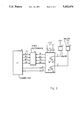
FIG. 1 is a block diagram of the embodiment; and
FIG. 2 is a block diagram of a control device having a switching arrangement in accordance with the invention.
DETAILED DESCRIPTION OF THE PREFERRED EMBODIMENT
In the figures, identical parts have been provided with the same reference numbers. The module 1 shown in FIG. 1 contains two identical circuits each having a semiconductor switch which is suitable as output stage (driver), for example, for different setting members in a motor vehicle and the circuits associated in each case with the semiconductor switch. In the following, therefore, only the circuit bearing the reference Nos. 2-29 will be described while the elements of the other circuit are provided with the reference Nos. 2' to 29' are understood to function in the same fashion.
The output stage is formed by a multi-emitter transistor 2, one emitter of which is connected to ground and the collector of which is connected to an output 3. Since the switching arrangement is intended essentially for the switching of inductive loads, a reverse-terminal protection diode 4 and free- wheeling zener diodes 5, 6 are connected in parallel to the transistor 2, the series-connected zener diodes 5, 6 furthermore providing protection against overvoltages for the transistor 2. By bridging the zener diode 5 by a transistor 7 the limiting voltage can be reduced.
A control signal for the transistor 2 is fed via an input 8 which is connected to ground via an input resistor 9. The control signal passes via a NAND gate 10, inverting amplifier 11, the amplification of which is adjustable, and a resistor 12 to the base of the transistor 2.
In order to recognize errors in the region of the output 3, an idle monitoring circuit and a short-circuit monitoring circuit are provided. The idle monitoring circuit responds when the current through the transistor 2 is below a predetermined threshold and when, therefore, an interruption in the line is present between the collector of the transistor 2, the load, within the load or between the load and the positive operating voltage. Furthermore, the idle monitoring circuit responds upon a short circuit of the output 3 with respect to ground.
The short-circuit monitoring circuit responds when the current through the transistor 2 exceeds another predetermined value which is the case essentially upon a connection between the output 3 or the line to the load on the one hand and the positive terminal of the source of operating voltage on the other hand.
The idle monitoring circuit is formed by a threshold value circuit 13, a low pass filter 14, a flip-flop 15, an OR gate 16 and an output transistor 17. From one output 18 there can be taken a signal which indicates idling.
The threshold value circuit 13 produces an output signal which is positive when a predetermined value of the current through the transistor 2 is exceeded. This predetermined value lies below the current to be expected for the load in question, in which connection tolerances of the individual loads and variations in time and temperature are to be taken into account. Brief disturbances are suppressed by the low pass filter 14 which has for instance a time constant of 200 μs.
The flip-flop 15 is set with the commencement in each case of a control pulse which brings the transistor 2 into the conductive state. The value L (low voltage) is then present at the output Q. Due to the OR connection at gate 16, with the control signal, which at this time has a value of H (high voltage), there is produced at the output of the OR gate 16 also a positive signal H which, via the resistor 19, places the transistor 17 into conductive state. The output 18 thus receives the level L.
If the current rises above the threshold value during the conductive phase of the transistor 2, which takes place in case of disturbance-free operation also in the case of inductive loads, the flip-flop 15 is reset. At the end of the conductive phase, the control signal assumes the value L so that as a result of the OR connection at gate 16 the signal at the output 18 is dependant on the level at the output Q. Since the flip-flop 15 has been reset, the level H is present at the output Q so that the transistor 17 continues to be conductive and the level L prevails at the output 18.
However, if the current through the transistor 2 has not exceeded the predetermined value during the conductive phase, the flip-flop 15 remains set so that the output Q continues to have the level L. This leads to a blocking of the transistor 17 so that the level L is outputted at the output 18 as error report.
A short-circuit monitoring circuit consists of a threshold value circuit 21, a low pass filter 22, an 0R gate 23, a flip-flop 24, and an output transistor 25 connected by resistor 29 to flip-flop 24, the collector of the transistor 25 serving as an output 26. The output signal of the threshold value circuit 21 jumps to a positive value if the current through the transistor 2 exceeds a value which lies above the currents to be expected upon normal operation. The low pass filter 22 serves to suppress brief disturbances. In order to counteract overloading of the transistor 2 as promptly as possible, the base of a transistor 28 is connected to the output of the threshold value circuit 21 via a resistor 27, the resistor 27 connecting the base of the transistor 28 to ground in the event of a short circuit and thus preventing further control. In this way, the current is limited to a value at which the transistor 2 is still not overloaded, and which current value is sufficient to set the flip-flop 24 which is clocked by the control signals.
By the setting of the flip flop 24, the transistor 25 which is connected via the resistor 29 with the output Q of the flip-flop 24 becomes conductive so that, in the event of a short circuit, the output 26 assumes the level L. At the same time, due to the connection of the output Q of the flip-flop 24 with the NAND gate 10, further feeding of the control signals to the transistor 2 is prevented until the control signal at the input 8 again changes from level L to level H and the flip-flop 24 is thus again reset.
In the module 1 there is furthermore provided a temperature sensor 31 which gives off a signal Thx which assumes the level H when a permissible value of temperature is exceeded. This signal is fed to the OR gates 23, 23' and thus produces a short-circuit error report in both circuits. Since a simultaneous short circuit of both outputs 3, 3' is extremely improbable, a connected microcomputer can recognize from this that with high probability a thermal overload is present.
Via a connection 32 the module 1 can be connected to ground potential or with the negative terminal of the source of operating voltage. A connection 33 serves to feed the positive operating voltage. By means of another connection 34, the module can be switched for two different load ranges. The connection 34 can be acted on by the positive operating voltage via a resistor 35.
If the module 1 is used in a control device with low loads, the connection 34 is connected to ground potential. In the case of control devices with high loads, the connection 34 remains without further connection. Via a non-inverting amplifier 36, the switch voltage PROG fed at 34 is fed to a control input of the amplifier 11 and control inputs of the threshold value circuits 13, 21. Via an inverting amplifier 37 the inverted switch voltage PROG passes to the base of the transistor 7. By the control of the amplifier 11 it is possible to adapt the base current of the transistor 2 to the corresponding load and therefore to the maximum current. In this way, an unnecessarily high base current in the case of smaller loads is avoided. The control of the threshold value circuits 13, 21 permits adaptation of the threshold values to the specific loads present. The switching of the voltage limitation can, for instance, be developed in such a manner that in the case of automotive fuel injection valves, which have a relatively high return voltage, the limitation is effected at 80 V and, in the case of other loads, at 27 V.
FIG. 2 shows parts of a control device using the module 1 of FIG. 1. In this case, a microcomputer 41 is provided which produces control signals and feeds them via the inputs 8, 8' to the module 1. The outputs 3, 3' of the module are connected with injection valves 42, 43 to which there is also fed a voltage of +12 V, which voltage may be applied also to one of the terminals or connections 33, 34. Via connections 33, 32 the module is connected to a source of operating voltage and to ground potential. For the scanning of the error reports which, as described in connection with FIG. 1, are produced in the module 1, the outputs 18, 26, 18', 26' are connected with inputs of a port extension 44. Via a data line 45 and corresponding control lines RD WR and CS the computer 41 scans the condition of the outputs 18, 26, 18' and 26'. If error reports are present, suitable steps can be introduced corresponding to the program entered in the computer 41.

Claims (14)

We claim:
1. A switching system suitable for driving automotive and automatic control devices and having a modular form, the system comprising
at least one semiconductor switch for switching a load; and
wherein each semiconductor switch comprises a multi-emitter transistor; and
for each semiconductor switch, the system further comprises a short-circuit monitoring circuit connected to a first emitter of said transistor and an idle monitoring circuit connected to a second emitter of said transistor, each of said monitoring circuits signaling a faulty value of load current in said transistor.
2. A system according to claim 1, wherein upon a pulsating control of said at least one semiconductor switch and upon a resultant current flow through said at least one semiconductor switch, said idle monitoring circuit produces an output signal indicative of idling
upon the occurrence of a value of said current flow which remains below a predetermined value during an entire conductive phase of said at least one semiconductor switch.
3. A system according to claim 2, wherein
said multi-emitter transistor includes a third emitter connected to ground.
4. A system according to claim 1, wherein
said idle monitoring circuit comprises a first threshold-value circuit connected to said at least one semiconductor switch for sensing current therein, a first low pass filter connected to an output of said first threshold valve circuit, and a first flip-flop connected to an output of said filter; and
wherein said short-circuit monitoring circuit comprises a second threshold-value circuit connected to said at least one semiconductor switch for sensing current therein, a second low pass filter connected to an output of said second threshold-value circuit, and a second flip-flop connected to said second low pass filter.
5. A system according to claim 4, wherein
said first flip-flop is resetable by an output signal of said first low pass filter and is set by a pulse control signal; and
an output signal of said first flip-flop is combined with said pulse control signal to form an output signal of said idle monitoring circuit.
6. A system according to claim 4, wherein
said second flip-flop is resetable by the output signal of said second low pass filter and is clock-controlled by a pulse control signal; and
an output signal of said second flip-flop serves as an output signal of said short-circuit monitoring circuit.
7. A system according to claim 6, wherein
said at least one semiconductor switch has a control electrode for receiving a control signal, said control signal inducing a current of flow through said at least one semiconductor switch; and
an output signal of said second threshold value circuit controls a feeding of said control signal to said control electrode of said at least one semiconductor switch.
8. A system according to claim 6, wherein
said at least one semiconductor switch has a control electrode for receiving a control signal, said control signal including a current of flow through said at least one semiconductor switch; and
a further another output signal of said second flip-flop controls a feeding of said control signal to said control electrode of said at least one semiconductor switch.
9. A system according to claim 4 further comprising
a power circuit connecting with each of said threshold-value circuits and with said transistor for adjusting operations of said threshold-value circuits and said transistor in accordance with a desired power level; and
wherein said power circuit includes a power input terminal for enabling said system to be operative with input power in different ranges of voltage magnitude.
10. A system according to claim 9, wherein
said at least one semiconductor switch has a control electrode for receiving a control signal, said control signal inducing a current of flow through said at least one semiconductor switch; and
the amplitude of said control signal applied to said control electrode of said at least one semiconductor switch is dependent on the voltage of said input power.
11. A system according to claim 9, wherein
threshold values to which said short circuit monitoring circuit and said idle monitoring circuit respond are dependent on the voltage of said input power.
12. A system according to claim 9, wherein
a limiting voltage at said first and said second threshold value circuits for said at least one semiconductor switch is dependent on the voltage of said input power.
13. A system according to claim 1, further comprising
a temperature sensor located in said module, an output signal of said sensor controlling said short-circuit monitoring circuits, wherein upon an exceeding of a predetermined temperature, each of said short-circuit monitoring circuits outputs an electric signal value indicating a short circuit in said load.
14. A switching system suitable for driving automotive and automatic control devices, comprising:
at least one semiconductor switching circuit for switching load current to a load, said switching circuit having a first branch and a second branch; and
wherein, for each semiconductor switching circuit, the system further comprises
a short circuit monitoring circuit connected to said first branch of said switching circuit for signaling a faulty value of the load current, and an idle monitoring circuit connected to said second branch of said switching circuit for signaling a faulty value of the load current.
US07/766,581 1990-10-31 1991-09-27 Switching system developed as module having at least one semiconductor switch for switching a load Expired - Fee Related US5262676A (en)

Applications Claiming Priority (2)

Application Number Priority Date Filing Date Title
DE4034569A DE4034569A1 (en) 1990-10-31 1990-10-31 CIRCUIT DESIGNED AS A BLOCK WITH AT LEAST ONE SEMICONDUCTOR SWITCH FOR SWITCHING A LOAD
DE4034569 1990-10-31

Publications (1)

Publication Number Publication Date
US5262676A true US5262676A (en) 1993-11-16

Family

ID=6417344

Family Applications (1)

Application Number Title Priority Date Filing Date
US07/766,581 Expired - Fee Related US5262676A (en) 1990-10-31 1991-09-27 Switching system developed as module having at least one semiconductor switch for switching a load

Country Status (3)

Country Link
US (1) US5262676A (en)
EP (1) EP0483450B1 (en)
DE (2) DE4034569A1 (en)

Cited By (4)

* Cited by examiner, † Cited by third party
Publication number Priority date Publication date Assignee Title
US5543997A (en) * 1992-12-17 1996-08-06 Erwin Sick Gmbh, Optik-Elektronik Safety switching system for a working apparatus
CN103837826A (en) * 2014-03-18 2014-06-04 国家电网公司 System and method for identification of faulty region of high-voltage switch operating circuit
CN103941155A (en) * 2014-04-09 2014-07-23 国家电网公司 High-voltage switch control loop break area identification circuit and identification method
US9647445B2 (en) * 2014-09-17 2017-05-09 Continental Automotive Systems, Inc. Over-current protection circuit and method

Families Citing this family (4)

* Cited by examiner, † Cited by third party
Publication number Priority date Publication date Assignee Title
EP0606160A1 (en) * 1993-01-08 1994-07-13 National Semiconductor Corporation Protection circuit used for deactivating a transistor during a short circuit having an inductive component
DE4317243C2 (en) * 1993-05-24 1997-10-02 Weidmueller Interface Coupling circuit
US5621603A (en) * 1995-07-26 1997-04-15 United Technologies Corporation Pulse width modulated solenoid driver controller
CN105425091B (en) * 2015-11-09 2018-07-27 上海凌翼动力科技有限公司 High-power circuit connects Resistance Fault dynamic simulator system and method, application

Citations (3)

* Cited by examiner, † Cited by third party
Publication number Priority date Publication date Assignee Title
US4114047A (en) * 1977-07-05 1978-09-12 Towmotor Corporation Control apparatus
US4349077A (en) * 1978-10-02 1982-09-14 Atsugi Motor Parts Co., Ltd. Electric control device for vehicle suspension system
US4809121A (en) * 1986-08-21 1989-02-28 Bayerische Motoren Werke Aktiengesellschaft Circuit arrangement in motor vehicles

Family Cites Families (8)

* Cited by examiner, † Cited by third party
Publication number Priority date Publication date Assignee Title
US4375073A (en) * 1980-06-16 1983-02-22 Reliance Electric Company Dual-monitoring protection circuit for switching transistor
DE3102267C2 (en) * 1981-01-24 1983-10-20 Licentia Patent-Verwaltungs-Gmbh, 6000 Frankfurt Arrangement for recording and evaluating the failure of ohmic consumers fed by current transformers
DE3150703C2 (en) * 1981-12-21 1985-07-04 Brown, Boveri & Cie Ag, 6800 Mannheim Control circuit for short-circuit proof output stages
DE3203513A1 (en) * 1982-01-29 1983-08-04 Licentia Patent-Verwaltungs-Gmbh, 6000 Frankfurt Device for intrinsically safe DC power supply of a transmission system
EP0197707A2 (en) * 1985-04-01 1986-10-15 Motorola, Inc. Electronic circuit breaker
JPH0630543B2 (en) * 1987-01-13 1994-04-20 株式会社東芝 Output circuit abnormality detection notification circuit
US4835652A (en) * 1988-07-06 1989-05-30 Westinghouse Electric Corp. Bi-directional DC power controller with fault protection
DE3842169A1 (en) * 1988-12-15 1990-06-28 Bosch Gmbh Robert Circuit arrangement with an FET output stage

Patent Citations (3)

* Cited by examiner, † Cited by third party
Publication number Priority date Publication date Assignee Title
US4114047A (en) * 1977-07-05 1978-09-12 Towmotor Corporation Control apparatus
US4349077A (en) * 1978-10-02 1982-09-14 Atsugi Motor Parts Co., Ltd. Electric control device for vehicle suspension system
US4809121A (en) * 1986-08-21 1989-02-28 Bayerische Motoren Werke Aktiengesellschaft Circuit arrangement in motor vehicles

Cited By (6)

* Cited by examiner, † Cited by third party
Publication number Priority date Publication date Assignee Title
US5543997A (en) * 1992-12-17 1996-08-06 Erwin Sick Gmbh, Optik-Elektronik Safety switching system for a working apparatus
CN103837826A (en) * 2014-03-18 2014-06-04 国家电网公司 System and method for identification of faulty region of high-voltage switch operating circuit
CN103837826B (en) * 2014-03-18 2016-08-24 国家电网公司 High-voltage switch gear operation circuit fault zone identification system and method
CN103941155A (en) * 2014-04-09 2014-07-23 国家电网公司 High-voltage switch control loop break area identification circuit and identification method
CN103941155B (en) * 2014-04-09 2018-06-05 国家电网公司 High-voltage switch gear control loop template domain identification circuit and discrimination method
US9647445B2 (en) * 2014-09-17 2017-05-09 Continental Automotive Systems, Inc. Over-current protection circuit and method

Also Published As

Publication number Publication date
EP0483450A1 (en) 1992-05-06
DE59108201D1 (en) 1996-10-24
EP0483450B1 (en) 1996-09-18
DE4034569A1 (en) 1992-05-07

Similar Documents

Publication Publication Date Title
US6031705A (en) Surge protection circuit, in particular for inputs of integrated circuits
EP0010882B1 (en) A switching circuit
US5623254A (en) Drive circuit fault detection drive
US4300508A (en) Installation for operating electromagnetic loads in internal combustion engines
EP0358972A1 (en) An electrical circuit, particularly an electronic power circuit for motor vehicle injection systems, with a function for the detection and diagnosis of faults, and method related thereto
US4623833A (en) Alternator system multifunction fault detector
US5262676A (en) Switching system developed as module having at least one semiconductor switch for switching a load
US4017765A (en) Short circuit protected electronic control system
EP0216816B1 (en) Circuit for dissipating stored inductive energy
EP1650845A2 (en) Load dump protection circuit
JPH04234544A (en) Load monitoring device for use in internal- combustion engine or vehicle
US5285345A (en) Modulator switching system having at least one semiconductor switch for adaptation to different load ranges and protection thresholds
WO1985005231A1 (en) Short detection circuit and method for an electrical load
US5424897A (en) Three leaded protected power device having voltage input
US5483635A (en) Circuit for protecting a load control device from high and low voltage conditions
US5479314A (en) Circuit arrangement having a semiconductor switch for the switching of a load
US5883441A (en) Seat and seat belt sequence circuit
JPH0326417B2 (en)
US4636620A (en) Temperature compensation injector control system
US4451778A (en) Short-circuit-resistant trigger circuit layout for an electrical consumer
USRE33941E (en) Power driver having short circuit protection
US4812732A (en) Control device for an a. c. generator for an automobile
US4280166A (en) Over-voltage protected solid-state ignition system
US6489778B2 (en) Fault current recognition in control units
US5546260A (en) Protection circuit used for deactivating a transistor during a short-circuit having an inductive component

Legal Events

Date Code Title Description
AS Assignment

Owner name: VDO ADOLF SCHINDLING AG, A CORP. OF GERMANY

Free format text: ASSIGNMENT OF ASSIGNORS INTEREST.;ASSIGNORS:BLUMEL, THOMAS;MEICHER, JOACHIM;LUKAS, BERNHARD;AND OTHERS;REEL/FRAME:005857/0386

Effective date: 19910919

Owner name: VDO ADOLF SCHINDLING AG, GERMANY

Free format text: ASSIGNMENT OF ASSIGNORS INTEREST;ASSIGNORS:BLUMEL, THOMAS;MEICHER, JOACHIM;LUKAS, BERNHARD;AND OTHERS;REEL/FRAME:005857/0386

Effective date: 19910919

REMI Maintenance fee reminder mailed
LAPS Lapse for failure to pay maintenance fees
FP Expired due to failure to pay maintenance fee

Effective date: 19971119

STCH Information on status: patent discontinuation

Free format text: PATENT EXPIRED DUE TO NONPAYMENT OF MAINTENANCE FEES UNDER 37 CFR 1.362