US5166647A - Low-noise oscillator - Google Patents
Low-noise oscillator Download PDFInfo
- Publication number
- US5166647A US5166647A US07/825,680 US82568092A US5166647A US 5166647 A US5166647 A US 5166647A US 82568092 A US82568092 A US 82568092A US 5166647 A US5166647 A US 5166647A
- Authority
- US
- United States
- Prior art keywords
- noise
- resonant circuit
- low
- oscillator
- circuit means
- Prior art date
- Legal status (The legal status is an assumption and is not a legal conclusion. Google has not performed a legal analysis and makes no representation as to the accuracy of the status listed.)
- Expired - Fee Related
Links
Images

Classifications
-
- H—ELECTRICITY
- H03—ELECTRONIC CIRCUITRY
- H03B—GENERATION OF OSCILLATIONS, DIRECTLY OR BY FREQUENCY-CHANGING, BY CIRCUITS EMPLOYING ACTIVE ELEMENTS WHICH OPERATE IN A NON-SWITCHING MANNER; GENERATION OF NOISE BY SUCH CIRCUITS
- H03B5/00—Generation of oscillations using amplifier with regenerative feedback from output to input
-
- H—ELECTRICITY
- H03—ELECTRONIC CIRCUITRY
- H03B—GENERATION OF OSCILLATIONS, DIRECTLY OR BY FREQUENCY-CHANGING, BY CIRCUITS EMPLOYING ACTIVE ELEMENTS WHICH OPERATE IN A NON-SWITCHING MANNER; GENERATION OF NOISE BY SUCH CIRCUITS
- H03B15/00—Generation of oscillations using galvano-magnetic devices, e.g. Hall-effect devices, or using superconductivity effects
-
- H—ELECTRICITY
- H03—ELECTRONIC CIRCUITRY
- H03B—GENERATION OF OSCILLATIONS, DIRECTLY OR BY FREQUENCY-CHANGING, BY CIRCUITS EMPLOYING ACTIVE ELEMENTS WHICH OPERATE IN A NON-SWITCHING MANNER; GENERATION OF NOISE BY SUCH CIRCUITS
- H03B2200/00—Indexing scheme relating to details of oscillators covered by H03B
- H03B2200/003—Circuit elements of oscillators
- H03B2200/0034—Circuit elements of oscillators including a buffer amplifier
-
- H—ELECTRICITY
- H03—ELECTRONIC CIRCUITRY
- H03B—GENERATION OF OSCILLATIONS, DIRECTLY OR BY FREQUENCY-CHANGING, BY CIRCUITS EMPLOYING ACTIVE ELEMENTS WHICH OPERATE IN A NON-SWITCHING MANNER; GENERATION OF NOISE BY SUCH CIRCUITS
- H03B2200/00—Indexing scheme relating to details of oscillators covered by H03B
- H03B2200/006—Functional aspects of oscillators
- H03B2200/0088—Reduction of noise
- H03B2200/009—Reduction of phase noise
-
- H—ELECTRICITY
- H03—ELECTRONIC CIRCUITRY
- H03B—GENERATION OF OSCILLATIONS, DIRECTLY OR BY FREQUENCY-CHANGING, BY CIRCUITS EMPLOYING ACTIVE ELEMENTS WHICH OPERATE IN A NON-SWITCHING MANNER; GENERATION OF NOISE BY SUCH CIRCUITS
- H03B2202/00—Aspects of oscillators relating to reduction of undesired oscillations
- H03B2202/01—Reduction of undesired oscillations originated from distortion in one of the circuit elements of the oscillator
- H03B2202/017—Reduction of undesired oscillations originated from distortion in one of the circuit elements of the oscillator the circuit element being a frequency determining element
-
- H—ELECTRICITY
- H03—ELECTRONIC CIRCUITRY
- H03B—GENERATION OF OSCILLATIONS, DIRECTLY OR BY FREQUENCY-CHANGING, BY CIRCUITS EMPLOYING ACTIVE ELEMENTS WHICH OPERATE IN A NON-SWITCHING MANNER; GENERATION OF NOISE BY SUCH CIRCUITS
- H03B2202/00—Aspects of oscillators relating to reduction of undesired oscillations
- H03B2202/02—Reduction of undesired oscillations originated from natural noise of the circuit elements of the oscillator
- H03B2202/025—Reduction of undesired oscillations originated from natural noise of the circuit elements of the oscillator the noise being coloured noise, i.e. frequency dependent noise
- H03B2202/027—Reduction of undesired oscillations originated from natural noise of the circuit elements of the oscillator the noise being coloured noise, i.e. frequency dependent noise the noise being essentially proportional to the inverse of the frequency, i.e. the so-called 1/f noise
-
- H—ELECTRICITY
- H03—ELECTRONIC CIRCUITRY
- H03B—GENERATION OF OSCILLATIONS, DIRECTLY OR BY FREQUENCY-CHANGING, BY CIRCUITS EMPLOYING ACTIVE ELEMENTS WHICH OPERATE IN A NON-SWITCHING MANNER; GENERATION OF NOISE BY SUCH CIRCUITS
- H03B2202/00—Aspects of oscillators relating to reduction of undesired oscillations
- H03B2202/07—Reduction of undesired oscillations through a cancelling of the undesired oscillation
- H03B2202/073—Reduction of undesired oscillations through a cancelling of the undesired oscillation by modifying the internal feedback of the oscillator
Definitions
- the present invention relates to an oscillator which has low noise, in particular low phase noise, in the vicinity of its center frequency.
- a typical oscillator comprises a resonator (usually, but not always an inductor and a capacitor), an amplifier, a limiter and a load.
- the resonator is driven by the amplifier, which supplies the resonator with energy. Part of the energy in the resonator is applied to the input of the amplifier through a feedback circuit in order to keep the resonator in oscillation.
- the resonator and the amplifier thus form a closed loop. The rest of the energy is applied to the load, for useful work.
- the output of the amplifier is greater than the sum of the power dissipated in the resonator, the power applied to the amplifier, and the power applied to the load. This is because all oscillators require a loop gain greater than unity in order to operate. An oscillator will not function if, at the oscillator frequency, the magnitude of the product of the gain of the amplifier and the feedback factor of the feedback circuit is less than unity. If the loop gain is less than unity, the oscillations will decay to zero. In theory, the oscillator will operate if the loop gain is exactly equal to one, the so-called Barkhausen condition. However, as a practical matter, an oscillator in which the loop gain is exactly unity is an abstraction which is completely unrealizable in practice. Therefore, a practical oscillator always has a loop gain slightly larger than one to ensure that, with incidental yet inevitable variations in circuit parameters, the loop gain does not fall below unity.
- a signal of one volt, for example, appearing initially at the input will, after a trip around the loop, appear at the input as a signal larger than one volt. After another trip around the loop, this larger signal will become still larger, and so on.
- the amplitude of the oscillator output will therefore continue to increase unless it is limited, either by a discrete limiting circuit or by non-linearities (either inherent or intentionally introduced) in the amplifier or the resonator themselves.
- the noise figure is constant and lowest for a given device. At higher frequencies, the noise begins to increase again with frequency. Moreover, even a good "linear" amplifier will have some residual non-linearity which frequency-mixes, or beats with, any noise energy coming into the amplifier. The load also feeds back Johnson noise to the resonator. To provide power to an output load requires more energy (i.e., higher gain) from the linear amplifier, which requires additional amplifier current which, in turn, produces more noise. Finally, a separate limiter introduces noise due to its limiting action. This can include both 1/f noise and broadband Johnson noise.
- phase noise is especially detrimental, in that it introduces spurious frequency components which limit the usefulness of the oscillator in many applications.
- the present invention is a low-noise oscillator comprising resonant circuit means for generating a signal at a desired frequency, linear amplifier means electrically connected to the resonant circuit means at first and second locations thereon, limiter means electrically connected to the resonant circuit means at a third location thereon, and buffer amplifier means for applying the signal generated by the resonant circuit means to a load and electrically connected to the resonant circuit means at a fourth location thereon.
- the first, second, third and fourth locations are selected to minimize impedance at 1/f frequencies from the locations to electrical ground and to minimize Johnson noise into the resonant circuit.
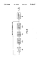
- FIG. 1 is a simplified schematic diagram of an oscillator according to the present invention.
- FIG. 2 is a simplified schematic representation of an equivalent circuit of a portion of the oscillator of FIG. 1.
- FIG. 3 is a simplified schematic diagram illustrating one way of realizing an oscillator according to the present invention.
- FIG. 1 a simplified schematic diagram of an oscillator 10 according to the invention.
- Oscillator 10 comprises a resonator 12, which is illustrated as an LC tank circuit composed of an inductor 14 and a capacitor 16.
- resonator 12 is shown as an LC tank circuit, it should be understood that any other type of resonator, such as a tuned cavity resonator, can be used without departing from the scope of the invention.
- a linear amplifier 18 is connected to and supplies energy to resonator 12.
- Linear amplifier is constrained to operate in its linear range to avoid introducing noise due to non-linear mixing into oscillator 10. By keeping linear amplifier 18 within its linear range, the effects of residual non-linearity (which result in frequency-mixing noise energy coming into the linear amplifier) are minimized.
- the oscillator is stabilized by a limiter 20, which can, for example, be composed of a pair of antiparallel diodes, although the limiter 20 is not restricted to this structure. Limiting may also be achieved by designing the resonator 12 to become non-linear and begin overloading at a specific circuit voltage.
- a portion of the energy of resonator 12 is applied to linear amplifier 18, where it is amplified and fed back to resonator 12.
- a portion of the energy is provided to limiter 20 and the remaining portion of the energy of resonator 12 is applied to a load 22, where it can be put to a desired use, such as a carrier for a modulator, a frequency reference, and so forth.
- Resonator 12 is isolated from load 22 by a buffer amplifier 24, to minimize noise feedback from the load and to minimize current loading of the resonator. It will be appreciated that a large load current demand on the resonator will require a greater current output from linear amplifier 18 which, in turn, tends to increase the noise introduced into oscillator 10.
- linear amplifier 18, limiter 20 and buffer amplifier 24 are all connected to coil 14 of resonator 12 at respective tap points T 1 through T 4 .
- T 1 , T 2 , T 3 and T 4 are shown in order of increasing distance from electrical ground, they need not be in that order, and may be located anywhere along coil 14 consistent with minimizing noise, as discussed below.
- Linear amplifier 18 is designed so that the noise that it introduces from its input circuit to the resonator is minimized, and so that the noise from the feedback circuit is also minimum. To accomplish this for a given linear amplifier, it is important to find the proper locations for the tap points on the resonator so that both the input to the amplifier and the output of the amplifier are optimized for minimum contribution to the noise circuit. Recognizing that both sources of noise contribution from the linear amplifier (the amplifier input circuit and the feedback circuit) contain 1/f noise, it becomes important to minimize the impedance to ground for both these respective tap points at frequencies (referred to herein as "1/f frequencies") at which 1/f noise is likely to be significant.
- 1/f frequencies frequencies
- the impedance to ground from a given tap point is schematically illustrated as a discrete inductor L T in series with a discrete resistor R T , connected between the tap point T and ground.
- Inductor L T represents the inductive component attributable to that portion of coil 14 which is physically and electrically between tap point T and ground
- resistor R T represents the resistive component of that portion of coil 14.
- R T is the resistance to ground and wL T is the inductive reactance to ground at 1/f frequencies. Both R T and L T for a superconductor can vary significantly at 1/f frequencies when compared to their values at oscillator frequency.
- the buffer amplifier input should be located at a tap point on coil 14 to optimize the following conditions: minimizing the impedance at 1/f frequencies between the input of the buffer amplifier and ground, minimize both the resistive loading of the tank circuit and the noise input to the tank circuit from the buffer amplifier, and keep the noise power added to the useful power passed to the load to be relatively negligible.
- the exact tap point may readily be located empirically.
- the high-Q tuned circuit 28 corresponds to resonator 12 in FIG. 1 and, like resonator 12, may be any high-Q resonator.
- high-Q tuned circuit 28 could be, but is not limited to, a tank circuit, a tuned cavity, or a cryogenic resonator, to give just a few examples.
- Low-noise linear amplifier stages 30A and 30B correspond to linear amplifier 18 in FIG. 1.
- FIG. 3 illustrates the low-noise linear amplifier as two separate stages 30A and 30B, but this is simply a design convenience, and the low-noise linear amplifier need not be so divided.
- the output of high-Q tuned circuit 28 is connected by a tap point, such as T 1 in FIG. 1, to the second stage 30B of the low-noise linear amplifier, in a manner as described in connection with FIG. 1, so as to optimize the minimum loading of the high-Q tuned circuit 28 while maximizing the oscillator signal-to-amplifier-noise ratio at the output of amplifier stage 30B.
- Low-noise buffer 32 which corresponds to buffer amplifier 24 in FIG. 1, is connected to the oscillator via a tap point such as T 4 , to minimize loading of the high-Q tuned circuit 28.
- Amplifier stage 30B acts to both buffer the loading effect of the low-noise buffer 32 itself and to increase the oscillator signal level into the buffer.
- the loading effect of the low-noise buffer 32 on the feedback loop must be minimized in order to minimize noise in the loop.
- the exact location of the tap point T 4 must be optimized as already described in connection with FIG. 1 to minimize noise in the feedback loop and maximize the oscillator-signal-to-buffer-amplifier-noise ratio in the output to the load.
- Limiter 34 corresponds to limiter 20 in FIG. 1. Optimally, limiter 34 maintains the maximum oscillator power so that the amplifiers stages 30A and 30B always operate in their linear ranges, while minimizing the limiter's own contribution to oscillator 1/f noise.
- the limiter 34 is the only non-linear element in the oscillator and, hence, the only element which can cause 1/f noise to mix with the noise present in the oscillator frequency range. This mixing can add significant noise close to the oscillator frequency. Care must be taken to ensure that the limiter does not cause amplitude-to-phase modulation conversion. This can be done by adjusting the limiter impedance at its operating point to match the RF source impedance in the feedback circuit.
- the circuit illustrated in FIG. 1 and the realization of the circuit shown in FIG. 3 are electrically the same.
- the physical difference is that, in the realization of FIG. 3, the limiter is buffered from the oscillator tuned circuit 28 by amplifier stage 30B.
- the present invention provides a novel and unobvious oscillator circuit which eliminates or greatly reduces sources of noise from a variety of sources, and which is therefore free from the problems associated with noisy oscillators.
Landscapes
- Inductance-Capacitance Distribution Constants And Capacitance-Resistance Oscillators (AREA)
Abstract
Description
Z=(R.sub.T.sup.2 +w.sup.2 L.sub.T).sup.1/2 (1)
Q=1/R[(L/C).sup.1/2 ] (2)
Claims (6)
Priority Applications (1)
| Application Number | Priority Date | Filing Date | Title |
|---|---|---|---|
| US07/825,680 US5166647A (en) | 1991-02-20 | 1992-01-27 | Low-noise oscillator |
Applications Claiming Priority (2)
| Application Number | Priority Date | Filing Date | Title |
|---|---|---|---|
| US07/658,285 US5118660A (en) | 1991-02-20 | 1991-02-20 | Superconducting low-noise oscillator |
| US07/825,680 US5166647A (en) | 1991-02-20 | 1992-01-27 | Low-noise oscillator |
Related Parent Applications (1)
| Application Number | Title | Priority Date | Filing Date |
|---|---|---|---|
| US07/658,285 Continuation-In-Part US5118660A (en) | 1991-02-20 | 1991-02-20 | Superconducting low-noise oscillator |
Publications (1)
| Publication Number | Publication Date |
|---|---|
| US5166647A true US5166647A (en) | 1992-11-24 |
Family
ID=27097599
Family Applications (1)
| Application Number | Title | Priority Date | Filing Date |
|---|---|---|---|
| US07/825,680 Expired - Fee Related US5166647A (en) | 1991-02-20 | 1992-01-27 | Low-noise oscillator |
Country Status (1)
| Country | Link |
|---|---|
| US (1) | US5166647A (en) |
Cited By (4)
| Publication number | Priority date | Publication date | Assignee | Title |
|---|---|---|---|---|
| US5268657A (en) * | 1992-07-10 | 1993-12-07 | Hughes Aircraft Company | High performance oscillator circuit with minimum frequency pulling at power on |
| US6157329A (en) * | 1997-09-15 | 2000-12-05 | Massachusetts Institute Of Technology | Bandpass sigma-delta modulator employing high-Q resonator for narrowband noise suppression |
| US6297708B1 (en) | 1999-02-18 | 2001-10-02 | Itron, Inc. | Temperature compensated high performance oscillator |
| US6489853B1 (en) | 2002-03-19 | 2002-12-03 | Z-Communications, Inc. | Low phase noise oscillator |
Citations (8)
| Publication number | Priority date | Publication date | Assignee | Title |
|---|---|---|---|---|
| US2704431A (en) * | 1949-01-17 | 1955-03-22 | Northrop Aircraft Inc | Stable resonant circuit |
| US3316499A (en) * | 1963-10-14 | 1967-04-25 | Zinn Stanley | Water cooled power oscillator |
| US3596203A (en) * | 1968-01-04 | 1971-07-27 | Nippon Electric Co | Plural transistor high frequency oscillator |
| US3617924A (en) * | 1968-04-17 | 1971-11-02 | Mitsubishi Electric Corp | Automatic frequency tuning system |
| US4290017A (en) * | 1978-12-26 | 1981-09-15 | Rockwell International Corporation | Apparatus and method for nondestructive evaluation of surface flaws in conductive materials |
| US4749963A (en) * | 1985-12-11 | 1988-06-07 | Matsushita Electric Industrial Co., Ltd. | Oscillator having stripline loop resonator |
| US4797614A (en) * | 1984-11-02 | 1989-01-10 | Sierracin Corporation | Apparatus and method for measuring conductance including a temperature controlled resonant tank circuit with shielding |
| US4901038A (en) * | 1987-12-30 | 1990-02-13 | Thomson Csf | Low-noise oscillator using superconducting nonlinear element |
-
1992
- 1992-01-27 US US07/825,680 patent/US5166647A/en not_active Expired - Fee Related
Patent Citations (8)
| Publication number | Priority date | Publication date | Assignee | Title |
|---|---|---|---|---|
| US2704431A (en) * | 1949-01-17 | 1955-03-22 | Northrop Aircraft Inc | Stable resonant circuit |
| US3316499A (en) * | 1963-10-14 | 1967-04-25 | Zinn Stanley | Water cooled power oscillator |
| US3596203A (en) * | 1968-01-04 | 1971-07-27 | Nippon Electric Co | Plural transistor high frequency oscillator |
| US3617924A (en) * | 1968-04-17 | 1971-11-02 | Mitsubishi Electric Corp | Automatic frequency tuning system |
| US4290017A (en) * | 1978-12-26 | 1981-09-15 | Rockwell International Corporation | Apparatus and method for nondestructive evaluation of surface flaws in conductive materials |
| US4797614A (en) * | 1984-11-02 | 1989-01-10 | Sierracin Corporation | Apparatus and method for measuring conductance including a temperature controlled resonant tank circuit with shielding |
| US4749963A (en) * | 1985-12-11 | 1988-06-07 | Matsushita Electric Industrial Co., Ltd. | Oscillator having stripline loop resonator |
| US4901038A (en) * | 1987-12-30 | 1990-02-13 | Thomson Csf | Low-noise oscillator using superconducting nonlinear element |
Cited By (5)
| Publication number | Priority date | Publication date | Assignee | Title |
|---|---|---|---|---|
| US5268657A (en) * | 1992-07-10 | 1993-12-07 | Hughes Aircraft Company | High performance oscillator circuit with minimum frequency pulling at power on |
| US6157329A (en) * | 1997-09-15 | 2000-12-05 | Massachusetts Institute Of Technology | Bandpass sigma-delta modulator employing high-Q resonator for narrowband noise suppression |
| US6297708B1 (en) | 1999-02-18 | 2001-10-02 | Itron, Inc. | Temperature compensated high performance oscillator |
| US6321074B1 (en) | 1999-02-18 | 2001-11-20 | Itron, Inc. | Apparatus and method for reducing oscillator frequency pulling during AM modulation |
| US6489853B1 (en) | 2002-03-19 | 2002-12-03 | Z-Communications, Inc. | Low phase noise oscillator |
Similar Documents
| Publication | Publication Date | Title |
|---|---|---|
| US5130675A (en) | Voltage-controlled oscillator | |
| US6297708B1 (en) | Temperature compensated high performance oscillator | |
| US7532080B2 (en) | LC oscillator circuit with a compensation coil for parasitical collector capacitor | |
| US4287489A (en) | Amplitude limited varactor tuned L-C oscillator | |
| US6768389B2 (en) | Integrated, digitally-controlled crystal oscillator | |
| US6466099B2 (en) | Voltage controlled oscillator (VCO) in colpitts configuration | |
| US4661785A (en) | Balanced feedback oscillators | |
| US4587497A (en) | Low-power low-harmonic transistor oscillator | |
| US4400660A (en) | Wide bandwidth high voltage regulator and modulator | |
| US20110193641A1 (en) | Low noise oscillators | |
| JP4182178B2 (en) | Oscillator | |
| US5422605A (en) | Low-noise push-pull crystal oscillator | |
| US20040032302A1 (en) | Low noise voltage controlled oscillator | |
| US5192875A (en) | Analog frequency divider utilizing two amplifiers and a LC resonant circuit | |
| US5166647A (en) | Low-noise oscillator | |
| US20050190003A1 (en) | Interpolative varactor voltage controlled oscillator with constant modulation sensitivity | |
| US6946908B1 (en) | Programmable radio frequency predistortion linearizer and method thereof | |
| US6091309A (en) | Tunable low noise oscillator using delay lines and ring mode trap filter | |
| US5118660A (en) | Superconducting low-noise oscillator | |
| US3845410A (en) | Crystal oscillator having spurious oscillation suppression circuit | |
| US7863993B1 (en) | Oscillator for providing oscillation signal with controllable frequency | |
| US4630004A (en) | Dielectric resonator stabilized microstrip oscillator | |
| US4001724A (en) | Variable high frequency crystal oscillator | |
| Alley et al. | An ultra-low noise microwave synthesizer | |
| JPH052001B2 (en) |
Legal Events
| Date | Code | Title | Description |
|---|---|---|---|
| AS | Assignment |
Owner name: AEL DEFENSE CORP., PENNSYLVANIA Free format text: ASSIGNMENT OF ASSIGNORS INTEREST.;ASSIGNOR:RIEBMAN, LEON;REEL/FRAME:005999/0474 Effective date: 19920123 |
|
| AS | Assignment |
Owner name: AEL INDUSTRIES, INC., PENNSYLVANIA Free format text: MERGER;ASSIGNOR:AEL DEFENSE CORP.;REEL/FRAME:006949/0868 Effective date: 19940226 |
|
| AS | Assignment |
Owner name: BANKERS TRUST COMPANY, NEW YORK Free format text: ASSIGNMENT FOR SECURITY;ASSIGNOR:AEL INDUSTRIES, INC.;REEL/FRAME:008085/0011 Effective date: 19960222 |
|
| REMI | Maintenance fee reminder mailed | ||
| LAPS | Lapse for failure to pay maintenance fees | ||
| FP | Lapsed due to failure to pay maintenance fee |
Effective date: 19961127 |
|
| AS | Assignment |
Owner name: AEL INDUSTRIES, INC., PENNSYLVANIA Free format text: RELEASE OF LIENS;ASSIGNOR:BANKERS TRUST COMPANY;REEL/FRAME:008401/0915 Effective date: 19970314 |
|
| STCH | Information on status: patent discontinuation |
Free format text: PATENT EXPIRED DUE TO NONPAYMENT OF MAINTENANCE FEES UNDER 37 CFR 1.362 |