US4991086A - Microprogram controlled microprocessor having a plurality of internal buses and including transfer register designation system - Google Patents
Microprogram controlled microprocessor having a plurality of internal buses and including transfer register designation system Download PDFInfo
- Publication number
- US4991086A US4991086A US07/217,197 US21719788A US4991086A US 4991086 A US4991086 A US 4991086A US 21719788 A US21719788 A US 21719788A US 4991086 A US4991086 A US 4991086A
- Authority
- US
- United States
- Prior art keywords
- coupled
- register
- transfer
- internal
- registers
- Prior art date
- Legal status (The legal status is an assumption and is not a legal conclusion. Google has not performed a legal analysis and makes no representation as to the accuracy of the status listed.)
- Expired - Lifetime
Links
Images


Classifications
-
- G—PHYSICS
- G06—COMPUTING; CALCULATING OR COUNTING
- G06F—ELECTRIC DIGITAL DATA PROCESSING
- G06F9/00—Arrangements for program control, e.g. control units
- G06F9/06—Arrangements for program control, e.g. control units using stored programs, i.e. using an internal store of processing equipment to receive or retain programs
- G06F9/22—Microcontrol or microprogram arrangements
- G06F9/226—Microinstruction function, e.g. input/output microinstruction; diagnostic microinstruction; microinstruction format
-
- G—PHYSICS
- G06—COMPUTING; CALCULATING OR COUNTING
- G06F—ELECTRIC DIGITAL DATA PROCESSING
- G06F15/00—Digital computers in general; Data processing equipment in general
- G06F15/76—Architectures of general purpose stored program computers
- G06F15/78—Architectures of general purpose stored program computers comprising a single central processing unit
- G06F15/7828—Architectures of general purpose stored program computers comprising a single central processing unit without memory
- G06F15/7832—Architectures of general purpose stored program computers comprising a single central processing unit without memory on one IC chip (single chip microprocessors)
Definitions
- the present invention relates to a microprogram transfer register designation system for use in a microprogram controlled microprocessor having a plurality of internal buses, and, the present invention relates more specifically to a microprogram transfer register designation system for designating, by one transfer register code, one set of source registers and destination registers which are respectively of the same number as that of the internal buses.
- microprogram control system includes a read only memory (ROM) provided internally in the microprocessor for storing a microprogram composed of a sequence of control codes (called "microcodes") and a microprogram sequencer for sequentially reading and decoding the microcodes from the ROM for each one word so as to control various hardware resources in the microprocessors.
- the internal hardware resources in the microprocessor includes various arithmetic logic units and registers, and each microprogram instructs various operations such as interregister data transfer, logic operations, condition decisions, branches, etc., similarly to machine languages for computers.
- microprogram execution speed is preferred over generality and descriptivity of programs, and therefore, each instruction has as many functions as possible which can be executed in parallel, such as a transfer instruction, an arithmetic operation instruction, a conditional branch and the like so that a parallel operation will be realized to the maximum extent, and therefore the hardware resources are efficiently utilized.
- the microprogram is different from the machine language for general computers. Accordingly, ordinary microcodes have a plurality of fields in one instruction so that different functions are described independently of one another.
- the microcodes are not so long and therefore, the microprogram control is very effective.
- the microcodes need a field of a long word length for designating the source registers and the destination registers for data transfers made by using the respective internal data buses.
- Another object of the present invention is to provide a microprogram transfer register designation system which is capable of executing the interregister transfer with a small number of steps.
- a microprogram transfer register designation system for a microprogram controlled microprocessor having a plurality of internal data buses, the system being such that there are previously prepared some number of source register sets each designating one source register for each of the internal buses and some number of destination register sets each designating one destination register for each of the internal buses, and then, there are selected one of the source register sets and one of the destination register sets when the interregister transfer is executed, wherein a transfer register designation field of a microcode includes a transfer inhibit flag for each of the internal buses.
- FIG. 1 is a block diagram of a typical conventional microprocessor having only one internal bus
- FIG. 2 illustrates a field structure of a microcode used in the microprocessor shown in FIG. 1;
- FIG. 3 is a block diagram of a typical conventional microprocessor having three internal buses
- FIG. 4 illustrates a field structure of a microcode used in the microprocessor shown in FIG. 3;
- FIG. 5 illustrates a field structure of a microcode used in the microprocessor shown in FIG. 3 in the case that transfer registers are previously combined into some number of sets;
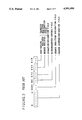
- FIG. 6 illustrates a field structure of one embodiment of a microcode for executing the transfer register designation method in accordance with the present invention.
- FIG. 7 is a block diagram of one embodiment of a microprocessor having three internal buses, which is capable of executing the transfer register designation method of the present invention in accordance with the microcode shown in FIG. 6.
- FIG. 1 there is shown a diagram of a typical conventional microprocessor having only one internal bus.
- the shown microprocessor comprises a pair of operand registers OPA and OPB coupled to an internal bus BUS so as to receive a pair of operands A and B, respectively.
- These operand registers OPA and OPB are coupled to a pair of inputs of an arithmetic logic unit ALU which in turn outputs the results of a designated operation to a operation result register RES coupled to the internal bus BUS.
- a communication register COMR coupled to an external data bus and a program counter PC coupled to an external address bus.
- a program status word PSW, a scratch pad register SPR and general registers GR0 and GR1 are coupled to the internal bus BUS.
- a source register and a designation register for interregister transfer can be designated as indicated in TABLE 1. Therefore, a field for designating the transfer registers needs three bits for each of the source register and the destination register. In addition, assuming that the operations designated for the ALU includes eight operations indicated in TABLE 2, a field for designating the operation of the ALU requires three bits.
- a microsequencer controls the operation in four manners, as indicated in TABLE 3, and one of eight conditions shown in TABLE 4 can be selected in the case of the conditional branch.
- the branch address can be designated by a relative address of an eight-bit displacement. Under these conditions, two bits are required for the microsequencer control field, and three bits and eight bits are needed for the branch condition designation field and the branch address designation field, respectively. Therefore, the field for controlling the operation of the microsequencer includes thirteen bits.
- the microprocessor shown in FIG. 1 uses the microcode of 22 bits having a field structure as shown in FIG. 2.
- the transfer register designation field needs only six bits in total which is sufficiently smaller than the total bit length of the microcode.
- the microcodes or microinstructions have to include a transfer field independently for each of the respective data buses.
- FIG. 3 there is shown a block diagram of a typical conventional microprocessor having three kinds of internal buses T, E and M.
- the shown microprocessor shown in FIG. 3 includes a main arithmetic logic unit MALU and an extra arithmetic logic unit EALU.
- the MALU includes a pair of inputs respectively coupled to a pair of operand registers MOPA and MOPB coupled to the internal bus M so as to receive a pair of operands A and B, respectively.
- An operation result register MRES coupled to an output of the arithmetic logic unit MALU is coupled to the internal bus M.
- the EALU includes a pair of inputs respectively coupled to a pair of operand registers EOPA and EOPB which are coupled to the internal buses E and T, respectively so as to receive a pair of operands A and B.
- An operation result register ERES coupled to an output of the EALU is coupled to the internal buses E and T, respectively.
- a communication register COMR coupled to an external data bus is coupled to the internal buses T, E and M, respectively, and a program counter PC coupled to an external address bus is coupled to the internal bus E.
- a scratch pad register TSPR and general registers TGR0 and MGR1 To the internal bus T there are coupled a scratch pad register TSPR and general registers TGR0 and MGR1.
- a program status word PSW is coupled to the internal buses E and T.
- the source registers and the destination registers which can be selected for the internal buses T, E and M in the case of interregister transfer are as indicated in the following TABLES 5, 6 and 7.
- a field for designating the source register and another field for designating the destination register respectively require three bits for each of a transfer using the but T, a transfer using the bus E and a transfer using the bus M. Namely, only the transfer register designation field needs 18 bits in total.
- the arithmetic logic unit is increased to two, in association with the operation designation field (TABLE 2) and the branch condition designation field (TABLE 4) an EALU/MALU selection flag and an ERES/MRES selection flag are required in order to indicate which is instructed to execute the operation, the main arithmetic logic unit MALU or the extra arithmetic logic unit EALU.
- the microcode has to have the instruction word length of 36 bits as illustrated in FIG. 4.
- one of the conventional microprogram control systems has proposed to previously prepare some number of source register sets each designating one source register for each of the internal buses and some number of destination register sets each designating one destination register for each of the internal buses, as shown in the following TABLE 8.
- one of the source register sets and one of the destination register sets are selected so that the contents of registers designated by the selected source register sets are transferred to registers designated by the destination source register sets, respectively. Accordingly, the source register designation fields included in one instruction (microcode) can be reduced to one field and the destination register designation fields can also be reduced to one field.
- FIG. 5 there is shown a field structure of one example of microcodes which can be used in the microprocessor shown in FIG. 3 in which the transfer registers are previously combined into some number of sets.
- the transfer register designation field is composed of eight bits as seen from TABLE 8. Namely, the 0th to 3rd bits form the destination register set field and the 4th to 7th bits form the source register set field. In addition, the 8th to 10th bits form the operation designation field for the extra arithmetic logic unit EALU or the main arithmetic logic unit MALU. The 11th bit is the EALU/MALU selection flag for indicating to which the operation designated by the operation designation field is directed, the extra arithmetic logic unit EALU or the main arithmetic logic unit MALU.
- the 12th and 13th bits form the microsequencer control field, and the 14th to 16th bits constitute the branch condition designation field for indicating a branch condition or a call condition in the case of the conditional branch or the subroutine call being designated by the microsequencer control field.
- the 17th bit is the ERES/MRES selection flag for indicating to which the condition designated by the branch condition designation field is directed, the register ERES or MRES.
- the 18th to 26th bits form the branch address designation field for indicating a head address of the branch destination and the subroutine in the case that the conditional branch or the subroutine call is designated by the microsequence control field.
- the microcode for the transfer register designation system has the word length of 26 bits.
- the data transfer is executed by using the buses T and M. Thereafter, the source register set of the code "0010" and the destination register set of the code "0111" are selected so that a second transfer is executed as follows:
- the transfer to the register EOPA is firstly executed (the first transfer) and then the content of the register EGRO is saved by using the register ESPR as a temporary save register (the second transfer). Thereafter, the data transfer is executed for the buses T and M (third transfer). As a result, the content of the register EGRO is destroyed, but the content saved in the register ESPR is returned to the register EGRO (fourth transfer). This sequence is very complicated and needs many transfer steps.
- the conventional improved transfer register designation system previously prepares some number of source register sets each designating one source register for each of the internal buses and some number of destination register sets each designating one destination register for each of the internal buses, and then, selects one of the source register sets and one of the destination register sets when the interregister transfer is executed.
- this system even if it is not required to transfer data between all the registers designated by one combination of source register set and destination register set, data transfer is executed between all the designated registers without exception. As a result, the content of an unintended destination register is destroyed.
- the microcode must be written to select a register whose content is allowed to be destroyed, as the register which will unintentionally be destroyed by the data transfer.
- FIG. 6 there is shown a field structure of a microcode written in accordance with the present invention for executing the above mentioned interregister transfer (1).
- the shown microcode written in accordance with the present invention includes a transfer inhibit flag provided for each of the internal buses M, T and E. With addition of three bits to the microcode, it is possible to prevent, in the course of register set transfer, the destruction of the content of the register which should not be destroyed.
- FIG. 7 there is shown a block diagram of one embodiment of the microprocessor having three internal buses, which is capable of executing the interregister transfer in accordance with the microcode shown in FIG. 6.
- elements similar to those shown in FIG. 3 are given the same reference signs, and explanation thereof will not be repeated.
- the shown microprocessor includes an instruction latch 10 for receiving an instruction from the external data bus, and an instruction decoder 12 coupled to the instruction latch 10.
- This instruction decoder 12 outputs start address information for a designated microprogram to a microprogram ROM (read only memory) 14 whose output is coupled to a microinstruction latch 16.
- ROM read only memory
- the lowest three bits of the latch 16 are coupled to a write address decoder 22 which generates write signals directed to destination registers indicated by the destination register set code.
- a write signal for the register TRGO is applied through an AND gate 24T to a write signal input of the register TGRO
- a write signal for the register ERGO is applied through an AND gate 24E to a write signal input of the register EGRO
- a write signal for the register MRGO is applied through an AND gate 24M to a write signal input of the register MRGO.
- the other write signals generated by the write address decoder 22 are applied to the other registers in a similar manner.
- the next lower three bits of the latch 16 are coupled to a read address decoder 20 which generates read signals directed to source registers indicated by the source register set code. These read signals are applied to the registers in a manner similar to the case of the write signals.
- each of the transfer inhibit flags is connected to the AND gates connected to the write signal inputs of all the registers coupled to the corresponding internal bus.
- the transfer inhibit flag for the bus T is connected to the other input of the AND gate 24T connected to the write signal input of the register TGRO.
- the transfer inhibit flag for the bus E is connected to the other input of the AND gate 24E connected to the write signal input of the register EGRO.
- the transfer inhibit flag for the bus M is connected to the other input of the AND gate 24M connected to the write signal input of the register MGRO.
Abstract
Description
              TABLE 1
______________________________________
SOURCE               DESTINATION
REGISTER   CODE      REGISTER     CODE
______________________________________
GR0        000       GR0          000
GR1        001       GR1          001
SPR        010       SPR          010
RES        011       OPA          011
--         --        OPB          100
PSW        101       PSW          101
PC         110       PC           110
COMR       111       COMR         111
______________________________________
              TABLE 2
______________________________________
OPERATION       CODE
______________________________________
NOP             000
INC             001
ADD             010
SUB             011
NOT             100
AND             101
OR              110
EXOR            111
______________________________________
TABLE 3 ______________________________________ CONDITION CODE ______________________________________ HALT 00 CONDITIONAL BRANCH 01CONDITIONAL SUBROUTINE CALL 10 RETURN FROMSUBROUTINE 11 ______________________________________
              TABLE 4
______________________________________
CONDITION             CODE
______________________________________
NO BRANCH             000
UNCONDITIONAL BRANCH  001
RES = 0               010
CARRY OF RES = 1      011
LSB OF RES = 1        100
MSB OF RES = 1        101
A TERMINAL = HIGH     110
B TERMINAL = HIGH     111
______________________________________
              TABLE 5
______________________________________
      SOURCE               DESTINATION
BUS   REGISTER    CODE     REGISTER   CODE
______________________________________
T     TGR0        000      TGR0       000
      TGR1        001      TGR1       001
      TSPR        010      TSPR       010
      ERES        011      EOPA       011
      --          --       EOPB       100
      PSW         101      PSW        101
      COMR        111      COMR       111
______________________________________
              TABLE 6
______________________________________
      SOURCE               DESTINATION
BUS   REGISTER    CODE     REGISTER   CODE
______________________________________
E     EGR0        000      EGR0       000
      EGR1        001      EGR1       001
      ESPR        010      ESPR       010
      ERES        011      EOPA       011
      --          --       EOPB       100
      PSW         101      PSW        101
      PC          110      PC         110
      COMR        111      COMR       111
______________________________________
              TABLE 7
______________________________________
      SOURCE               DESTINATION
BUS   REGISTER    CODE     REGISTER   CODE
______________________________________
M     MGR0        000      MGR0       000
      MGR1        001      MGR1       001
      MSPR        010      MSPR       010
      MRES        011      MOPA       011
      --          --       MOPB       100
      PC          110      PC         110
      COMR        111      COMR       111
______________________________________
                                  TABLE 8
__________________________________________________________________________
SOURCE             DESTINATION
REGISTER SET       REGISTER SET
T BUS
     E BUS
          M BUS
               CODE
                   T BUS
                        E BUS
                             M BUS
                                  CODE
__________________________________________________________________________
TGR0 EGR0 MGR0 0000
                   TGR0 EGR0 MGR0 0000
TGR1 EGR1 EGR1 0001
                   TGR1 EGR1 MGR1 0001
TSPR ESPR MSPR 0010
                   TSPR ESPR MSPR 0010
ERES ERES MRES 0011
                   NOS* EOPA MOPA 0011
TGR0 EGR0 MSPR 0100
                   NOS* EOPB MOPB 0100
TGR0 ESPR MGR0 0101
                   NOS* NOS* MOPA 0101
TSPR EGR0 MGR0 0110
                   NOS* NOS* MOPB 0110
TGR0 EGR0 MRES 0111
                   NOS* EOPA NOS* 0111
TGR0 ERES MGR0 1000
                   NOS* EOPB NOS* 1000
ERES EGR0 MGR0 1001
                   EOPA NOS* NOS* 1001
TSPR ESPR MRES 1010
                   EOPB NOS* NOS* 1010
TSPR ERES MSPR 1011
                   NOS* PSW  NOS* 1011
ERES ESPR MSPR 1100
                   COMR PC   NOS* 1100
ERES PSW  COMR 1101
                   NOS* NOS* COMR 1101
ERES COMR MRES 1110
                   NOS* COMR NOS* 1110
COMR PC   MRES 1111
                   NOS* NOS* NOS* 1111
__________________________________________________________________________
 *NOS is an abbreviation of "no select" which means that no destinatin
 register is designated.
ERES=TGRO; ERES=EGRO and MRES=MGRO (first transfer) . . . (2)
TSPR=NOS; ESPR=EOPA and MSPR=NOS (second transfer) . . . (3)
TSPR=NOS; ESPR=EOPA and MRES=NOS (second transfer) . . . (3) Accordingly, when the first transfer register set code is decoded, the ANDgate 24E associated to the register EGRO is blocked and therefore the content of the register EGRO is maintained as it is. Thus, the desired interegister data transfer can be executed without destroying the content of the register EGRO and with a small number of steps.
Claims (4)
Applications Claiming Priority (2)
| Application Number | Priority Date | Filing Date | Title |
|---|---|---|---|
| JP62-172142 | 1987-07-09 | ||
| JP62172142A JPH0648461B2 (en) | 1987-07-09 | 1987-07-09 | Microprogram transfer register specification method |
Publications (1)
| Publication Number | Publication Date |
|---|---|
| US4991086A true US4991086A (en) | 1991-02-05 |
Family
ID=15936343
Family Applications (1)
| Application Number | Title | Priority Date | Filing Date |
|---|---|---|---|
| US07/217,197 Expired - Lifetime US4991086A (en) | 1987-07-09 | 1988-07-11 | Microprogram controlled microprocessor having a plurality of internal buses and including transfer register designation system |
Country Status (5)
| Country | Link |
|---|---|
| US (1) | US4991086A (en) |
| EP (1) | EP0298523B1 (en) |
| JP (1) | JPH0648461B2 (en) |
| KR (1) | KR940002322B1 (en) |
| DE (1) | DE3888740T2 (en) |
Cited By (7)
| Publication number | Priority date | Publication date | Assignee | Title |
|---|---|---|---|---|
| US5303354A (en) * | 1991-07-08 | 1994-04-12 | Mitsubishi Denki Kabushiki Kaisha | Data transfer system between registers for microcomputer |
| US5481728A (en) * | 1993-07-02 | 1996-01-02 | Mitsubishi Denki Kabushiki Kaisha | Data processor having circuitry for high speed clearing of an interrupt vector register corresponding to a selected interrupt request |
| US5657484A (en) * | 1990-04-26 | 1997-08-12 | Sgs-Thomson Microelectronics S.R.L. | Method for carrying out a boolean operation between any two bits of any two registers |
| US5687344A (en) * | 1991-05-08 | 1997-11-11 | Hitachi, Ltd. | Single-chip microcomputer having an expandable address area |
| US5802346A (en) * | 1995-06-02 | 1998-09-01 | International Business Machines Corporation | Method and system for minimizing the delay in executing branch-on-register instructions |
| US5809259A (en) * | 1993-11-08 | 1998-09-15 | Hitachi, Ltd. | Semiconductor integrated circuit device |
| US20100332704A1 (en) * | 2009-06-26 | 2010-12-30 | Renesas Electronics Corporation | Semiconductor device and serial interface circuit |
Families Citing this family (2)
| Publication number | Priority date | Publication date | Assignee | Title |
|---|---|---|---|---|
| US4988500A (en) * | 1989-09-29 | 1991-01-29 | The Procter & Gamble Company | Oral compositions |
| WO1998006038A1 (en) * | 1996-08-07 | 1998-02-12 | Sun Microsystems, Inc. | Architectural support for software pipelining of loops |
Citations (12)
| Publication number | Priority date | Publication date | Assignee | Title |
|---|---|---|---|---|
| US3644901A (en) * | 1969-07-24 | 1972-02-22 | Univ Iowa State | Digital system for controlling signal transfers between registers and data buses |
| US3932841A (en) * | 1973-10-26 | 1976-01-13 | Raytheon Company | Bus controller for digital computer system |
| US3938098A (en) * | 1973-12-26 | 1976-02-10 | Xerox Corporation | Input/output connection arrangement for microprogrammable computer |
| US4133030A (en) * | 1977-01-19 | 1979-01-02 | Honeywell Information Systems Inc. | Control system providing for the transfer of data in a communications processing system employing channel dedicated control blocks |
| US4342078A (en) * | 1979-05-21 | 1982-07-27 | Motorola, Inc. | Instruction register sequence decoder for microprogrammed data processor and method |
| US4347566A (en) * | 1978-12-11 | 1982-08-31 | Tokyo Shibaura Denki Kabushiki Kaisha | Data processor with register file and arithmetic logic circuit on one chip and register means directly connected to the chip |
| US4412283A (en) * | 1980-05-30 | 1983-10-25 | Fairchild Camera & Instrument Corp. | High performance microprocessor system |
| US4482953A (en) * | 1980-05-30 | 1984-11-13 | Fairchild Camera & Instrument Corporation | Computer with console addressable PLA storing control microcode and microinstructions for self-test of internal registers and ALU |
| US4509115A (en) * | 1982-04-21 | 1985-04-02 | Digital Equipment Corporation | Two-port memory controller |
| US4597074A (en) * | 1982-07-27 | 1986-06-24 | Cselt, Centro Studi E Laboratori Telecomunicazioni Spa | Multichannel interface linking a PCM line with a processor |
| US4719568A (en) * | 1982-12-30 | 1988-01-12 | International Business Machines Corporation | Hierarchical memory system including separate cache memories for storing data and instructions |
| US4833640A (en) * | 1985-10-25 | 1989-05-23 | Hitachi, Ltd. | Register bank change including register to register transfer in a data processing system |
Family Cites Families (3)
| Publication number | Priority date | Publication date | Assignee | Title |
|---|---|---|---|---|
| US4014006A (en) * | 1973-08-10 | 1977-03-22 | Data General Corporation | Data processing system having a unique cpu and memory tuning relationship and data path configuration |
| FR2253435A5 (en) * | 1973-11-30 | 1975-06-27 | Honeywell Bull Soc Ind | |
| DE2529348A1 (en) * | 1975-07-01 | 1977-01-13 | Siemens Ag | METHOD FOR PROCESSING MACHINE COMMANDS WITH BYTE FIELD OPERANDS IN A MICROPROGRAMMED PROCESSOR OF A DATA PROCESSING SYSTEM |
-
1987
- 1987-07-09 JP JP62172142A patent/JPH0648461B2/en not_active Expired - Fee Related
-
1988
- 1988-07-09 KR KR1019880008584A patent/KR940002322B1/en not_active IP Right Cessation
- 1988-07-11 DE DE3888740T patent/DE3888740T2/en not_active Expired - Fee Related
- 1988-07-11 EP EP88111074A patent/EP0298523B1/en not_active Expired - Lifetime
- 1988-07-11 US US07/217,197 patent/US4991086A/en not_active Expired - Lifetime
Patent Citations (12)
| Publication number | Priority date | Publication date | Assignee | Title |
|---|---|---|---|---|
| US3644901A (en) * | 1969-07-24 | 1972-02-22 | Univ Iowa State | Digital system for controlling signal transfers between registers and data buses |
| US3932841A (en) * | 1973-10-26 | 1976-01-13 | Raytheon Company | Bus controller for digital computer system |
| US3938098A (en) * | 1973-12-26 | 1976-02-10 | Xerox Corporation | Input/output connection arrangement for microprogrammable computer |
| US4133030A (en) * | 1977-01-19 | 1979-01-02 | Honeywell Information Systems Inc. | Control system providing for the transfer of data in a communications processing system employing channel dedicated control blocks |
| US4347566A (en) * | 1978-12-11 | 1982-08-31 | Tokyo Shibaura Denki Kabushiki Kaisha | Data processor with register file and arithmetic logic circuit on one chip and register means directly connected to the chip |
| US4342078A (en) * | 1979-05-21 | 1982-07-27 | Motorola, Inc. | Instruction register sequence decoder for microprogrammed data processor and method |
| US4412283A (en) * | 1980-05-30 | 1983-10-25 | Fairchild Camera & Instrument Corp. | High performance microprocessor system |
| US4482953A (en) * | 1980-05-30 | 1984-11-13 | Fairchild Camera & Instrument Corporation | Computer with console addressable PLA storing control microcode and microinstructions for self-test of internal registers and ALU |
| US4509115A (en) * | 1982-04-21 | 1985-04-02 | Digital Equipment Corporation | Two-port memory controller |
| US4597074A (en) * | 1982-07-27 | 1986-06-24 | Cselt, Centro Studi E Laboratori Telecomunicazioni Spa | Multichannel interface linking a PCM line with a processor |
| US4719568A (en) * | 1982-12-30 | 1988-01-12 | International Business Machines Corporation | Hierarchical memory system including separate cache memories for storing data and instructions |
| US4833640A (en) * | 1985-10-25 | 1989-05-23 | Hitachi, Ltd. | Register bank change including register to register transfer in a data processing system |
Non-Patent Citations (2)
| Title |
|---|
| Motorola, MC68020 32 Bit Microprocessor Users Manual, 1985 (1 2, 1 3, 2 1, 2 2, 2 5, B 91). * |
| Motorola, MC68020 32-Bit Microprocessor Users Manual, 1985 (1-2, 1-3, 2-1, 2-2, 2-5, B-91). |
Cited By (9)
| Publication number | Priority date | Publication date | Assignee | Title |
|---|---|---|---|---|
| US5657484A (en) * | 1990-04-26 | 1997-08-12 | Sgs-Thomson Microelectronics S.R.L. | Method for carrying out a boolean operation between any two bits of any two registers |
| US5687344A (en) * | 1991-05-08 | 1997-11-11 | Hitachi, Ltd. | Single-chip microcomputer having an expandable address area |
| US5303354A (en) * | 1991-07-08 | 1994-04-12 | Mitsubishi Denki Kabushiki Kaisha | Data transfer system between registers for microcomputer |
| US5481728A (en) * | 1993-07-02 | 1996-01-02 | Mitsubishi Denki Kabushiki Kaisha | Data processor having circuitry for high speed clearing of an interrupt vector register corresponding to a selected interrupt request |
| US5809259A (en) * | 1993-11-08 | 1998-09-15 | Hitachi, Ltd. | Semiconductor integrated circuit device |
| US5930488A (en) * | 1993-11-08 | 1999-07-27 | Hitachi, Ltd. | Semiconductor integrated circuit device with a central processing unit, a data transfer controller and a memory storing data transfer parameters |
| US5802346A (en) * | 1995-06-02 | 1998-09-01 | International Business Machines Corporation | Method and system for minimizing the delay in executing branch-on-register instructions |
| US20100332704A1 (en) * | 2009-06-26 | 2010-12-30 | Renesas Electronics Corporation | Semiconductor device and serial interface circuit |
| US8601187B2 (en) * | 2009-06-26 | 2013-12-03 | Renesas Electronics Corporation | Semiconductor device and serial interface circuit |
Also Published As
| Publication number | Publication date |
|---|---|
| EP0298523A3 (en) | 1989-11-08 |
| EP0298523A2 (en) | 1989-01-11 |
| DE3888740D1 (en) | 1994-05-05 |
| JPH0648461B2 (en) | 1994-06-22 |
| JPS6415826A (en) | 1989-01-19 |
| KR890002766A (en) | 1989-04-11 |
| EP0298523B1 (en) | 1994-03-30 |
| DE3888740T2 (en) | 1994-09-29 |
| KR940002322B1 (en) | 1994-03-23 |
Similar Documents
| Publication | Publication Date | Title |
|---|---|---|
| EP0996057B1 (en) | Data processor with an instruction unit having a cache and a ROM | |
| US4454578A (en) | Data processing unit with pipelined operands | |
| US5922065A (en) | Processor utilizing a template field for encoding instruction sequences in a wide-word format | |
| US4825355A (en) | Instruction format for program control type data processing systems | |
| US3990052A (en) | Central processing unit employing microprogrammable control for use in a data processing system | |
| JPH0926878A (en) | Data processor | |
| JPS6339931B2 (en) | ||
| JPH06332792A (en) | Data processor, data reading control circuit thereof and data writing control circuit | |
| US5682531A (en) | Central processing unit | |
| US4005391A (en) | Peripheral interrupt priority resolution in a micro program data processor having plural levels of subinstruction sets | |
| USRE32493E (en) | Data processing unit with pipelined operands | |
| JPS62197830A (en) | Data processing system | |
| US7546442B1 (en) | Fixed length memory to memory arithmetic and architecture for direct memory access using fixed length instructions | |
| US4323964A (en) | CPU Employing micro programmable control for use in a data processing system | |
| US5097407A (en) | Artificial intelligence processor | |
| US4991086A (en) | Microprogram controlled microprocessor having a plurality of internal buses and including transfer register designation system | |
| US4430711A (en) | Central processing unit | |
| US4789957A (en) | Status output for a bit slice ALU | |
| US4763246A (en) | Microprogram control | |
| EP0035334B1 (en) | Data processing system with two level microprogramming | |
| US5889984A (en) | Floating point and integer condition compatibility for conditional branches and conditional moves | |
| US4771376A (en) | Processor | |
| US4245327A (en) | Data processor having two types of carry flags | |
| JPH0642198B2 (en) | Data processing device | |
| JP3102399B2 (en) | Data processing apparatus and method |
Legal Events
| Date | Code | Title | Description |
|---|---|---|---|
| AS | Assignment |
Owner name: NEC CORPORATION, 33-1, SHIBA 5-CHOME, MINATO-KU, T Free format text: ASSIGNMENT OF ASSIGNORS INTEREST.;ASSIGNOR:KOJIMA, SHINGO;REEL/FRAME:004956/0776 Effective date: 19880803 Owner name: NEC CORPORATION,JAPAN Free format text: ASSIGNMENT OF ASSIGNORS INTEREST;ASSIGNOR:KOJIMA, SHINGO;REEL/FRAME:004956/0776 Effective date: 19880803 |
|
| STCF | Information on status: patent grant |
Free format text: PATENTED CASE |
|
| FEPP | Fee payment procedure |
Free format text: PAYOR NUMBER ASSIGNED (ORIGINAL EVENT CODE: ASPN); ENTITY STATUS OF PATENT OWNER: LARGE ENTITY |
|
| FPAY | Fee payment |
Year of fee payment: 4 |
|
| FEPP | Fee payment procedure |
Free format text: PAYOR NUMBER ASSIGNED (ORIGINAL EVENT CODE: ASPN); ENTITY STATUS OF PATENT OWNER: LARGE ENTITY |
|
| FPAY | Fee payment |
Year of fee payment: 8 |
|
| FPAY | Fee payment |
Year of fee payment: 12 |
|
| AS | Assignment |
Owner name: NEC ELECTRONICS CORPORATION, JAPAN Free format text: ASSIGNMENT OF ASSIGNORS INTEREST;ASSIGNOR:NEC CORPORATION;REEL/FRAME:013758/0440 Effective date: 20021101 |