US4901317A - Efficient maximum-likelihood decoder for the golay (24,12) code - Google Patents
Efficient maximum-likelihood decoder for the golay (24,12) code Download PDFInfo
- Publication number
- US4901317A US4901317A US07/231,125 US23112588A US4901317A US 4901317 A US4901317 A US 4901317A US 23112588 A US23112588 A US 23112588A US 4901317 A US4901317 A US 4901317A
- Authority
- US
- United States
- Prior art keywords
- inner product
- values
- subcode
- maximum likelihood
- set forth
- Prior art date
- Legal status (The legal status is an assumption and is not a legal conclusion. Google has not performed a legal analysis and makes no representation as to the accuracy of the status listed.)
- Expired - Fee Related
Links
Images

Classifications
-
- H—ELECTRICITY
- H03—ELECTRONIC CIRCUITRY
- H03M—CODING; DECODING; CODE CONVERSION IN GENERAL
- H03M13/00—Coding, decoding or code conversion, for error detection or error correction; Coding theory basic assumptions; Coding bounds; Error probability evaluation methods; Channel models; Simulation or testing of codes
- H03M13/03—Error detection or forward error correction by redundancy in data representation, i.e. code words containing more digits than the source words
- H03M13/05—Error detection or forward error correction by redundancy in data representation, i.e. code words containing more digits than the source words using block codes, i.e. a predetermined number of check bits joined to a predetermined number of information bits
- H03M13/13—Linear codes
- H03M13/15—Cyclic codes, i.e. cyclic shifts of codewords produce other codewords, e.g. codes defined by a generator polynomial, Bose-Chaudhuri-Hocquenghem [BCH] codes
- H03M13/1505—Golay Codes
-
- H—ELECTRICITY
- H03—ELECTRONIC CIRCUITRY
- H03M—CODING; DECODING; CODE CONVERSION IN GENERAL
- H03M13/00—Coding, decoding or code conversion, for error detection or error correction; Coding theory basic assumptions; Coding bounds; Error probability evaluation methods; Channel models; Simulation or testing of codes
- H03M13/37—Decoding methods or techniques, not specific to the particular type of coding provided for in groups H03M13/03 - H03M13/35
- H03M13/45—Soft decoding, i.e. using symbol reliability information
Definitions
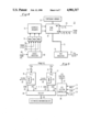
- Another general object of the present invention is to basically divide the inner product chip into eight cells, each of which performs decoding for sixteen cosets.
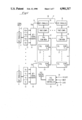
- a first segment is provided for receiving serial data and loading the data into bit-parallel registers in the precomputational chip.
- data circuits in the precomputational chip calculate and store information employed for the decoding operation.
- the inner product chip calculates the inner products and their corresponding code words.
- select circuits in the inner product chip determine the final estimated code word.
- FIG. 6 is a more detailed block diagram of the add and compare circuits in the processing elements of FIG. 5;
- FIG. 9 is a detailed block diagram of the structure employed to determine the proper sign bits in the IPC chip.
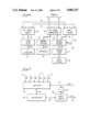
- the information in bit parallel register 18 is two's complemented in complementer 25 before being stored in SG 1 temporary memory 26.
- the information in memory 26 is supplied to one ofthe eight SG 1 registers 27 etc. 28 as a result of the output from bit register 14 adding the different combinations supplied by registers X 1 to X 4 .
- a two-phase clock is supplied to the system controller19 on line 29.
- the master reset signal on line 31 and load signal on line 32 are supplied from the inner product circuit which will be explained later.
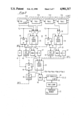
- FIG. 2 is a more detailed block diagram of the bit serial adder 14 shown in FIG. 1. It will be understood that each of the bit serial adders 14 shown in FIG. 2 includes individual bit serial adders33, 34 and 35. To maintain correlation between FIG. 1 and FIG. 2, the registers shown as four bit registers are numbered X 21 to X 24 , similar to the register 13 in FIG. 1. The output of the four X I registers are applied directly to exclusive OR gates 36, 37 and 38 or bit serial adder 34 to perform the addition functions.
- bit parallel register 16 which receives a SG load signal on line 49 from the PCC controller.
- the value inthe bit parallel register 16 is stored in temporary memory 22 in its two's complement form without a sign change.
- the temporary memory 22 holds one of the eight possible combinations of the value SG 6 until it is stored in one of the eight RAM registers 23 etc. 24 shown in FIG. 1.
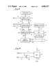
- the preferred embodiment precomputational circuit system controller 19 operates under the control of external timing signals generated at clock 51 and load logic circuit 52which are connected to the counters 53 to 56 that produce control signals like the control signals T 1 , T 2 and T 3 on the output control busses 57 to 61.
- the outputs of the counter on control busses 57 to 61 are applied to the combinatorial circuit logic to provide the necessary PCC control signals on bus 63 which provide the necessary control and timing signals for the PCC system.
- the counters 53 to 56 are enabled by the MRST signal on line 31 operating in conjunction with the enable flip-flops 64, 65 and 66.
- RAM storage element 67 is loaded from temporary memory 22 under control of the control signals from system controller 19 and the signals which originate at bus 63.
- the information in RAM 67 is accessed or read by first loading coset register 68 with information from the inner product circuit (IPC) and one of the lines 69 therefrom.
- An address is generated out of address decoder 71 under controlof the control signals R1 to R3 and the output of coset register 68 operating in conjunction with the multiplexers 72.
- the information being read from RAM 67 is presented on bus 73 and stored in Out register 74 before being supplied as an SG value on line 75 to the inner product circuit shown in FIG. 5.
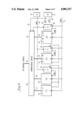
- FIG. 6 is a more detailed block diagram of one of the subsystems which perform the add and compare functions in the processing elements 76 and 77.
- the elements 76 comprise bit serial adders 88 which add the magnitudes of the SG1 through SG6 inputs on lines 75 to produce a sigma output on line 89 which is stored in sigma latch 91 until called forby the IPC circuits.
- the bit serial comparators 92 are employed to determine the SG K value which has the minimum magnitude and stores that value in minimum register 93 until called for by the IPC controller.
- FIG. 7 is a more detailed block diagram of the parity checker 95 shown in FIG. 6.
- the SG K input line 75 are shown as inputsto the sign latch 99 which produces the signs of the SG K 's on output bus 101 which is stored in the sign register 102.
- the information in sign register 102 is applied to the parity counter 103 via line 104 to produce a stored parity count shown as the parity flag (PFLAG) on output line 98.
- An initialization signal INIT2 from the IP system control bus 87 is shown being applied to sign latch 99 and also through delay 105 to parity counter 103 to produce the pority flag output signal on line 98.
- FIG. 8 is a more detailed block diagram of the bit serial comparators 92 and the subcode decoders 94 shown in FIG. 6.
- the same input lines 75 which are shown in FIGS. 6 and 7 are shown in FIG. 8 as inputs to the bank of comparators 106 and the bit parallel register 107.
- the bank of comparators 106 determine the minimum magnitude of the SG K 's and supply this information on bus 108 to the minimum decoder 109 which holds this value in the decode register 109.
- the minimum value in the decode register 109 is supplied to subcode decoder 94 which also has a sign input on line 111.
- the subcode decoder 94 provides outputs on lines 112 etc.
- the inner product calculator supplies a signal via line 127 to the main decoder 122 to determine the proper subcode code word to be stored in coderegister 126.
- the control and timing of storing the inner product and code word in register 124 and 126 are under control of the final load signal onone of the control lines 87 described hereinbefore.
Abstract
Description
Claims (18)
Priority Applications (1)
| Application Number | Priority Date | Filing Date | Title |
|---|---|---|---|
| US07/231,125 US4901317A (en) | 1988-08-11 | 1988-08-11 | Efficient maximum-likelihood decoder for the golay (24,12) code |
Applications Claiming Priority (1)
| Application Number | Priority Date | Filing Date | Title |
|---|---|---|---|
| US07/231,125 US4901317A (en) | 1988-08-11 | 1988-08-11 | Efficient maximum-likelihood decoder for the golay (24,12) code |
Publications (1)
| Publication Number | Publication Date |
|---|---|
| US4901317A true US4901317A (en) | 1990-02-13 |
Family
ID=22867835
Family Applications (1)
| Application Number | Title | Priority Date | Filing Date |
|---|---|---|---|
| US07/231,125 Expired - Fee Related US4901317A (en) | 1988-08-11 | 1988-08-11 | Efficient maximum-likelihood decoder for the golay (24,12) code |
Country Status (1)
| Country | Link |
|---|---|
| US (1) | US4901317A (en) |
Cited By (7)
| Publication number | Priority date | Publication date | Assignee | Title |
|---|---|---|---|---|
| US20070113159A1 (en) * | 2005-11-16 | 2007-05-17 | Ismail Lakkis | Golay-code generation |
| US20070168841A1 (en) * | 2005-11-16 | 2007-07-19 | Ismail Lakkis | Frame format for millimeter-wave systems |
| US20070245221A1 (en) * | 2005-11-16 | 2007-10-18 | Ismail Lakkis | Multi-mode processor |
| US20080075176A1 (en) * | 2006-09-25 | 2008-03-27 | Alfred E. Mann Foundation For Scientific Research | Rotationally invariant non-coherent burst coding |
| US20080298435A1 (en) * | 2006-11-30 | 2008-12-04 | Ismail Lakkis | Common Air Interface Supporting Single Carrier and OFDM |
| US20090100316A1 (en) * | 2007-10-10 | 2009-04-16 | Qualcomm Incorporated | Method and apparatus for generation and usage of extended golay codes |
| US20090110031A1 (en) * | 2007-10-10 | 2009-04-30 | Qualcomm Incorporated | Millimeter wave beaconing with directional antennas |
Citations (4)
| Publication number | Priority date | Publication date | Assignee | Title |
|---|---|---|---|---|
| US4397022A (en) * | 1981-01-30 | 1983-08-02 | Weng Ming I | Weighted erasure codec for the (24, 12) extended Golay code |
| US4414667A (en) * | 1981-11-27 | 1983-11-08 | Gte Products Corporation | Forward error correcting apparatus |
| US4613860A (en) * | 1983-12-14 | 1986-09-23 | Sperry Corporation | Coder-decoder for purged binary block codes |
| US4648091A (en) * | 1984-07-02 | 1987-03-03 | General Electric Company | Apparatus and method for decoding error correction coded information |
-
1988
- 1988-08-11 US US07/231,125 patent/US4901317A/en not_active Expired - Fee Related
Patent Citations (4)
| Publication number | Priority date | Publication date | Assignee | Title |
|---|---|---|---|---|
| US4397022A (en) * | 1981-01-30 | 1983-08-02 | Weng Ming I | Weighted erasure codec for the (24, 12) extended Golay code |
| US4414667A (en) * | 1981-11-27 | 1983-11-08 | Gte Products Corporation | Forward error correcting apparatus |
| US4613860A (en) * | 1983-12-14 | 1986-09-23 | Sperry Corporation | Coder-decoder for purged binary block codes |
| US4648091A (en) * | 1984-07-02 | 1987-03-03 | General Electric Company | Apparatus and method for decoding error correction coded information |
Non-Patent Citations (2)
| Title |
|---|
| Hackett, C. M., "An Efficient Algorithm for Soft-Decision Decoding of the (24,12) Extended Golay Code", IEEE Transactions on Communications, vol. Com, 29, No. 6, Jun. 1981. |
| Hackett, C. M., An Efficient Algorithm for Soft Decision Decoding of the (24,12) Extended Golay Code , IEEE Transactions on Communications, vol. Com, 29, No. 6, Jun. 1981. * |
Cited By (24)
| Publication number | Priority date | Publication date | Assignee | Title |
|---|---|---|---|---|
| US20090097533A1 (en) * | 2005-11-16 | 2009-04-16 | Qualcomm Incorporated | Method and apparatus for single carrier spreading |
| US20070168841A1 (en) * | 2005-11-16 | 2007-07-19 | Ismail Lakkis | Frame format for millimeter-wave systems |
| US20070245221A1 (en) * | 2005-11-16 | 2007-10-18 | Ismail Lakkis | Multi-mode processor |
| US8910027B2 (en) * | 2005-11-16 | 2014-12-09 | Qualcomm Incorporated | Golay-code generation |
| US8724676B2 (en) | 2005-11-16 | 2014-05-13 | Qualcomm Incorporated | Method and apparatus for single carrier spreading |
| US8583995B2 (en) | 2005-11-16 | 2013-11-12 | Qualcomm Incorporated | Multi-mode processor |
| US8418040B2 (en) * | 2005-11-16 | 2013-04-09 | Qualcomm Incorporated | Method and apparatus for single carrier and OFDM sub-block transmission |
| US20090100317A1 (en) * | 2005-11-16 | 2009-04-16 | Qualcomm Incorporated | Method and apparatus for single carrier and ofdm sub-block transmission |
| US8527853B2 (en) | 2005-11-16 | 2013-09-03 | Qualcomm Incorporated | Golay-code generation |
| US20090204874A9 (en) * | 2005-11-16 | 2009-08-13 | Qualcomm Incorporated | Method and apparatus for single carrier and ofdm sub-block transmission |
| US8429502B2 (en) | 2005-11-16 | 2013-04-23 | Qualcomm Incorporated | Frame format for millimeter-wave systems |
| US20110209035A1 (en) * | 2005-11-16 | 2011-08-25 | Qualcomm Incorporated | Golay-code generation |
| US20070113159A1 (en) * | 2005-11-16 | 2007-05-17 | Ismail Lakkis | Golay-code generation |
| US8095849B1 (en) * | 2006-09-25 | 2012-01-10 | Alfred E. Mann Foundation For Scientific Research | Rotationally invariant non-coherent burst coding and decoding |
| US8099647B1 (en) * | 2006-09-25 | 2012-01-17 | Alfred E. Mann Foundation For Scientific Research | Rotationally invariant non-coherent burst coding mapping function |
| US8095850B1 (en) * | 2006-09-25 | 2012-01-10 | Alfred E. Mann Foundation For Scientific Research | Rotationally invariant non-coherent burst coding and decoding |
| US7779332B2 (en) * | 2006-09-25 | 2010-08-17 | Alfred E. Mann Foundation For Scientific Research | Rotationally invariant non-coherent burst coding |
| US20080075176A1 (en) * | 2006-09-25 | 2008-03-27 | Alfred E. Mann Foundation For Scientific Research | Rotationally invariant non-coherent burst coding |
| US8332732B2 (en) * | 2006-11-30 | 2012-12-11 | Qualcomm Incorporated | Common air interface supporting single carrier and OFDM |
| US20080298435A1 (en) * | 2006-11-30 | 2008-12-04 | Ismail Lakkis | Common Air Interface Supporting Single Carrier and OFDM |
| US8472497B2 (en) | 2007-10-10 | 2013-06-25 | Qualcomm Incorporated | Millimeter wave beaconing with directional antennas |
| US20090110031A1 (en) * | 2007-10-10 | 2009-04-30 | Qualcomm Incorporated | Millimeter wave beaconing with directional antennas |
| US20090100316A1 (en) * | 2007-10-10 | 2009-04-16 | Qualcomm Incorporated | Method and apparatus for generation and usage of extended golay codes |
| US8856628B2 (en) | 2007-10-10 | 2014-10-07 | Qualcomm Incorporated | Method and apparatus for generation and usage of extended golay codes |
Similar Documents
| Publication | Publication Date | Title |
|---|---|---|
| US3961750A (en) | Expandable parallel binary shifter/rotator | |
| US4852048A (en) | Single instruction multiple data (SIMD) cellular array processing apparatus employing a common bus where a first number of bits manifest a first bus portion and a second number of bits manifest a second bus portion | |
| US6728743B2 (en) | Modulo remainder generator | |
| US3943494A (en) | Distributed execution processor | |
| EP0234147A2 (en) | Two-wire/three-port RAM for cellular array processor | |
| US4901317A (en) | Efficient maximum-likelihood decoder for the golay (24,12) code | |
| JPH03129427A (en) | Data maintainability feature of sorting accelerator | |
| US5251321A (en) | Binary to binary coded decimal and binary coded decimal to binary conversion in a VLSI central processing unit | |
| US4188669A (en) | Decoder for variable-length codes | |
| US3938087A (en) | High speed binary comparator | |
| US7296048B2 (en) | Semiconductor circuit for arithmetic processing and arithmetic processing method | |
| JPH0250492B2 (en) | ||
| US4538238A (en) | Method and apparatus for calculating the residue of a signed binary number | |
| US4162535A (en) | Triangular high speed I/O system for content addressable memories | |
| US4153943A (en) | High speed I/O for content addressable type memories | |
| US5126965A (en) | Conditional-sum carry structure compiler | |
| US4751665A (en) | Systolic super summation device | |
| US4604723A (en) | Bit-slice adder circuit | |
| US3591784A (en) | Real time digital fourier analyzer | |
| US6240540B1 (en) | Cyclic redundancy check in a computer system | |
| US3113204A (en) | Parity checked shift register counting circuits | |
| US3742459A (en) | Data processing method and apparatus adapted to sequentially pack error correcting characters into memory locations | |
| US3564505A (en) | Digital data reordering system | |
| Abbaszadeh et al. | VLSI implementation of a maximum-likelihood decoder for the Golay (24, 12) code | |
| US3140464A (en) | Central parity checker operating from and into a data transfer bus |
Legal Events
| Date | Code | Title | Description |
|---|---|---|---|
| AS | Assignment |
Owner name: UNISYS CORPORATION, TOWNSHIP LINE AND UNION MEETIN Free format text: ASSIGNMENT OF ASSIGNORS INTEREST.;ASSIGNORS:RUSHFORTH, CRAIG K.;ABBASZADEH, AYYOOB D.;REEL/FRAME:004952/0897 Effective date: 19880810 |
|
| FEPP | Fee payment procedure |
Free format text: PAYOR NUMBER ASSIGNED (ORIGINAL EVENT CODE: ASPN); ENTITY STATUS OF PATENT OWNER: LARGE ENTITY |
|
| FPAY | Fee payment |
Year of fee payment: 4 |
|
| FEPP | Fee payment procedure |
Free format text: PAYER NUMBER DE-ASSIGNED (ORIGINAL EVENT CODE: RMPN); ENTITY STATUS OF PATENT OWNER: LARGE ENTITY |
|
| FEPP | Fee payment procedure |
Free format text: PAYOR NUMBER ASSIGNED (ORIGINAL EVENT CODE: ASPN); ENTITY STATUS OF PATENT OWNER: LARGE ENTITY |
|
| FPAY | Fee payment |
Year of fee payment: 8 |
|
| AS | Assignment |
Owner name: L-3 COMMUNICATIONS CORPORATION, NEW YORK Free format text: ASSIGNMENT OF ASSIGNORS INTEREST;ASSIGNOR:LOCKHEED MARTIN CORPORATION, A CORP. OF MD;REEL/FRAME:010180/0073 Effective date: 19970430 |
|
| AS | Assignment |
Owner name: LORAL CORPORATION, MARYLAND Free format text: ASSIGNMENT OF ASSIGNORS INTEREST;ASSIGNOR:UNISYS CORPORATION;REEL/FRAME:010547/0468 Effective date: 19950505 |
|
| AS | Assignment |
Owner name: LOCKHEED MARTIN TACTICAL SYSTEMS, INC., MARYLAND Free format text: CHANGE OF NAME;ASSIGNOR:LORAL CORP.;REEL/FRAME:010639/0395 Effective date: 19960423 |
|
| AS | Assignment |
Owner name: LOCKHEED MARTIN CORP., MARYLAND Free format text: MERGER;ASSIGNOR:LOCKHEED MARTIN TACTICAL SYSTEMS, INC.;REEL/FRAME:010742/0857 Effective date: 19970627 |
|
| REMI | Maintenance fee reminder mailed | ||
| LAPS | Lapse for failure to pay maintenance fees | ||
| STCH | Information on status: patent discontinuation |
Free format text: PATENT EXPIRED DUE TO NONPAYMENT OF MAINTENANCE FEES UNDER 37 CFR 1.362 |
|
| FP | Lapsed due to failure to pay maintenance fee |
Effective date: 20020213 |