US4900917A - Polarization insensitive optical communication device utilizing optical preamplification - Google Patents

Polarization insensitive optical communication device utilizing optical preamplification Download PDF

Info

Publication number
US4900917A
US4900917A US07/219,684 US21968488A US4900917A US 4900917 A US4900917 A US 4900917A US 21968488 A US21968488 A US 21968488A US 4900917 A US4900917 A US 4900917A
Authority
US
United States
Prior art keywords
optical
polarization
amplified
signal
component
Prior art date
Legal status (The legal status is an assumption and is not a legal conclusion. Google has not performed a legal analysis and makes no representation as to the accuracy of the status listed.)
Expired - Lifetime
Application number
US07/219,684
Inventor
Melvyn Dixon
Nils A. Olsson
Robert E. Tench
Liang Tzeng
Current Assignee (The listed assignees may be inaccurate. Google has not performed a legal analysis and makes no representation or warranty as to the accuracy of the list.)
AMERICAN TELEPHONE AND TELEGRAPH COMPANY AT&T BELL LABORATORIES
AT&T Corp
Original Assignee
AMERICAN TELEPHONE AND TELEGRAPH COMPANY AT&T BELL LABORATORIES
Priority date (The priority date is an assumption and is not a legal conclusion. Google has not performed a legal analysis and makes no representation as to the accuracy of the date listed.)
Filing date
Publication date
Application filed by AMERICAN TELEPHONE AND TELEGRAPH COMPANY AT&T BELL LABORATORIES filed Critical AMERICAN TELEPHONE AND TELEGRAPH COMPANY AT&T BELL LABORATORIES
Priority to US07/219,684 priority Critical patent/US4900917A/en
Assigned to AMERICAN TELEPHONE AND TELEGRAPH COMPANY, 550 MADISON AVENUE, NEW YORK, NEW YORK 10022-3201, A CORP. OF NEW YORK, BELL TELEPHONE LABORATORIES, INCORPORATED, 600 MOUNTAIN AVENUE, MURRAY HILL, NEW JERSEY, 07974-2070, U.S.A., A CORP. OF NEW YORK reassignment AMERICAN TELEPHONE AND TELEGRAPH COMPANY, 550 MADISON AVENUE, NEW YORK, NEW YORK 10022-3201, A CORP. OF NEW YORK ASSIGNMENT OF ASSIGNORS INTEREST. Assignors: DIXON, MELVYN, TENCH, ROBERT E., TZENG, LIANG, OLSSON, NILS A.
Priority to EP19890306857 priority patent/EP0351133A3/en
Priority to CA000605666A priority patent/CA1293997C/en
Priority to JP1180642A priority patent/JPH02134624A/en
Application granted granted Critical
Publication of US4900917A publication Critical patent/US4900917A/en
Anticipated expiration legal-status Critical
Expired - Lifetime legal-status Critical Current

Links

Images

Classifications

    • HELECTRICITY
    • H04ELECTRIC COMMUNICATION TECHNIQUE
    • H04BTRANSMISSION
    • H04B10/00Transmission systems employing electromagnetic waves other than radio-waves, e.g. infrared, visible or ultraviolet light, or employing corpuscular radiation, e.g. quantum communication
    • H04B10/60Receivers
    • H04B10/66Non-coherent receivers, e.g. using direct detection
    • H04B10/67Optical arrangements in the receiver
    • H04B10/671Optical arrangements in the receiver for controlling the input optical signal
    • H04B10/672Optical arrangements in the receiver for controlling the input optical signal for controlling the power of the input optical signal
    • H04B10/673Optical arrangements in the receiver for controlling the input optical signal for controlling the power of the input optical signal using an optical preamplifier
    • HELECTRICITY
    • H04ELECTRIC COMMUNICATION TECHNIQUE
    • H04BTRANSMISSION
    • H04B10/00Transmission systems employing electromagnetic waves other than radio-waves, e.g. infrared, visible or ultraviolet light, or employing corpuscular radiation, e.g. quantum communication
    • H04B10/27Arrangements for networking
    • H04B10/272Star-type networks or tree-type networks
    • HELECTRICITY
    • H04ELECTRIC COMMUNICATION TECHNIQUE
    • H04BTRANSMISSION
    • H04B10/00Transmission systems employing electromagnetic waves other than radio-waves, e.g. infrared, visible or ultraviolet light, or employing corpuscular radiation, e.g. quantum communication
    • H04B10/60Receivers
    • H04B10/66Non-coherent receivers, e.g. using direct detection
    • H04B10/69Electrical arrangements in the receiver

Landscapes

  • Engineering & Computer Science (AREA)
  • Physics & Mathematics (AREA)
  • Electromagnetism (AREA)
  • Computer Networks & Wireless Communication (AREA)
  • Signal Processing (AREA)
  • Computing Systems (AREA)
  • Optical Communication System (AREA)

Abstract

A polarization insensitive optical device is disclosed which is capable of providing direct optical amplification of an input signal of unknown (and possibly varying) polarization. A polarization diversity technique is utilized wherein a polarization beam splitter is used to divide the incoming signal into orthogonal components of known polarization (TE,TM). The orthogonal components are then separately amplified, using a semiconductor laser as the amplifying device. The amplified components are then recombined, either optically or electrically, to form the final output signal.

Description

BACKGROUND OF THE INVENTION
1. Field of the Invention
The present invention relates to a polarization insensitive optical communication device utilizing optical preamplification and, more particularly, to such a device which uses polarization diversity to provide improved optical amplification.
2. Description of the Prior Art
In a conventional direct detection optical communication scheme, a message signal originates from a semiconductor light emitting source, travels over a length of optical fiber, and impinges the active region of a semiconductor photodetector. For many applications, this relatively simple system is satisfactory. However, at high bit rates (>4 Gb/s, for example), the coupling efficiency of the system degrades significantly, with a sensitivity of only -26 dBm at 8 Gb/s transmission (with a 10-9 bit error rate (BER)). Most high bit rate systems require a sensitivity of at least -32 dBm. A solution to this problem is to provide optical amplification at the input of the photodetector. That is, preamplify the optical signal before it enters the photodiode. One method of achieving this preamplification is to transform the optical signal into an electrical form (with a conventional photodiode, for example), perform standard electrical amplification with any of the various methods well-known in the art, then reconvert the amplified electrical signal into an amplified optical signal at the input of the receiver photodiode. In theory, this is a workable solution. In practice, however, the need to perform these optical-electrical and electrical-optical conversions has been found to seriously degrade the quality of the message signal. Further, these systems often require rather sophisticated and expensive electrical components.
A preferable solution is to perform optical amplification directly upon the message signal. As discussed in the article "Wideband 1.5 μm Optical Receiver Using Traveling-Wave Laser Amplifier", by M. J. O'Mahony et al. appearing in Electron Letters, No. 22, 1986 at pp. 1238-9, conventional lasers may be used to perform this optical amplification. Although this is considered an improvement, there still exists a problem with these devices in that they are sensitive to the state of polarization of the incoming light signal. In particular, due to the difference in confinement factors in the laser structure, the TE and TM polarization states may exhibit a difference in gain of approximately 10 dB. Such a polarization dependence is undesirable for optical amplifiers utilized with installed optical fiber-based communication networks, where the polarization state of the message signal is at best unknown, and at worst varies as a function of time.
Thus, a need remains in the prior art for achieving optical amplification which is truly polarization insensitive.
BRIEF DESCRIPTION OF THE DRAWING
Referring now to the drawings, where like numerals represent like parts in several views:
FIG. 1 is a block diagram of an exemplary polarization insensitive arrangement of the present invention;
FIG. 2 illustrates a polarization insensitive direct detection receiver utilizing the exemplary arrangement of FIG. 1;
FIG. 3 illustrates an exemplary receiver configuration for use in the direct detection scheme of FIG. 2;
FIG. 4 illustrates an exemplary in-line optical amplifier utilizing the arrangement of FIG. 1; and
FIG. 5 illustrates a wavelength division multiplexer (WDM) coherent communication scheme utilizing the in-line optical amplifier of FIG. 4.
DETAILED DESCRIPTION
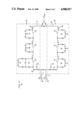
A simplified block diagram of the proposed polarization insensitive scheme of the present invention is illustrated in FIG. 1. As shown, an incoming optical signal IIN with an unknown polarization state is applied as an input to a polarization beam splitter 10 which functions to split signal IIN into two separate components having known polarizations. In particular, polarization beam splitter 10 functions to form a first component consisting of a TE polarized signal, denoted ITE, and a second component consisting of a TM polarized signal, denoted ITM. Polarization beam splitter 10 subsequently directs the first component ITE into a first section 12 of a polarization maintaining waveguide (polarization maintaining fiber, for example) and the second component ITM into a second section 14 of polarization maintaining waveguide. Thus, regardless of the state of polarization of signal IIN, the component propagating along waveguide section 12 will always be of a first, known state (TE) and similarly, the component propagating along waveguide section 14 will always be of the orthogonal state (TM).
First signal component ITE is subsequently applied as an input to a first optical amplifier 16, optical amplifier 16 being a laser amplifier of the type described in the O'Mahony et al. article mentioned above. It has been observed that the typical semiconductor laser which is utilized as a laser amplifier, a CSBH laser, for example, will exhibit a gain of approximately 25 dB when the incoming signal is polarized in the TE mode, as compared with a lesser gain of approximately 15-22 dB with a TM polarized incoming signal. Therefore, to obtain the maximum gain from first laser amplifier 16, amplifier 16 is oriented such that its TE axis is aligned with signal component ITE. As illustrated in FIG. 1, with this alignment, first optical amplifier 16 is defined as exhibiting a gain of G1 such that the output from optical amplifier 16 is G1 *ITE =I'TE.
In a similar fashion, second component ITM is also amplified. Referring to the particular arrangement of FIG. 1, second component ITM is redirected 90° by a mirror element 18 into a second optical amplifier 20. As mentioned above, a laser amplifier will exhibit the most gain when the incoming signal is polarized along the TE axis. Thus, second laser amplifier 20 is oriented such that its TE axis is orthogonal to the direction of propagation of second component ITM and parallel to the electric field vector of second component ITM. As illustrated in FIG. 1, second optical amplifier 20 exhibits a gain factor G2 such that the output from second optical amplifier 20 is defined as G2 *ITM =I'TM. As will be discussed in detail hereinafter in association with FIG. 2, it is preferred that the gain G1 of first amplifier 16 be identical to the gain G2 of second amplifier 20. This requirement is relatively easy to accomplish when the amplifiers are simultaneously fabricated on the same substrate. When this is the case, the gains will be relatively identical and will track each other as a function of both temperature and time. Otherwise, the DC drive currents applied to lasers 16 and 20 may be individually adjusted to equalize their gain.
Subsequent to the amplification, first component I'TE is directed along a waveguide 22 into a combiner element 26. Similarly, second component I'TM is directed along a waveguide 24 into combiner element 26. As will be described in detail hereinafter, combiner 26 performs either an electrical recombination of components I'TE and I'TM so as to form an electrical voltage output signal VOUT, or an optical recombination of components I'TE and I'TM so as to form an optical output signal IOUT. An optical recombination is performed when the arrangement of FIG. 1 is utilized as an in-line optical amplifier (for either direct detection or coherent communication systems), as discussed in association with FIGS. 4 and 5. Alternatively, an electrical recombination is performed when the arrangement of FIG. 1 is utilized as the receiver portion of a direct detection communication system, as discussed in detail below in association with FIGS. 2 and 3.
It is to be noted that for the polarization insensitive arrangement of FIG. 1, the performance of first optical amplifier 16 and second optical amplifier 20 may be degraded by reflections as discussed in the O'Mahony article mentioned above. Such reflections may be caused by imperfect performance of polarization beam splitter 10, polarization maintaining waveguides 12, 14, 22 and 24 or mirror element 18. Such reflections may also be caused by imperfect performance of optical components prior to polarization beam splitter 10, or subsequent to combiner 26 when optical recombination is employed. To optimize the performance of optical amplifiers 16 and 20 in FIG. 1, and in subsequent arrangements of FIG. 2 and FIG. 4, isolators may be employed. Faraday optical isolators are known in the art as exemplary devices capable of performing optical isolation. The isolators may be fabricated using either bulk optics or integrated optics techniques. The need for optical isolators, the number and specific design of isolators to be employed and the location of such isolators with respect to optical amplifiers 16,20 will be apparent to those skilled in the art.
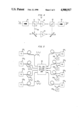
An exemplary direct detection receiver 30 utilizing the arrangement of FIG. 1 is illustrated in FIG. 2. As previously described, the input to receiver 30 is an optical signal IIN comprising an unknown (and usually varying with time) polarization state. This signal is first applied as an input to polarization beam splitter 10 which functions as described above to separate IIN into two components of known, orthogonal polarizations, ITE and ITM. First component ITE, as shown in FIG. 2, follows along branch 1 and is coupled into a polarization maintaining waveguide, illustrated in this embodiment as a section of polarization maintaining fiber 120, where fiber 120 directs component ITE into first laser amplifier 16. Similarly, signal component ITM, following along branch 2, is coupled into a section of polarization maintaining fiber 140 and subsequently applied as an input to second laser amplifier 20. It is to be understood that various lensing arrangements may be used to couple polarization maintaining fibers 120,140 to amplifiers 16,20, and that polarization maintaining waveguides of other forms could be utilized, where in some embodiments a reflecting element, such as mirror 18 of FIG. 1, would be required to redirect one of the signal components into its associated laser amplifier.
Devices currently utilized as laser amplifiers are known to exhibit spontaneous-spontaneous beat noise which seriously degrades the quality of the amplified output signal. To solve this problem, bandpass filters may be placed at the exit of such amplifiers to minimize this noise factor. Thus, referring to FIG. 2, amplified signal I'TE exiting first laser amplifier 16 is subsequently applied as an input to a first optical bandpass filter 32. First filter 32 is chosen to comprise a sufficiently narrow bandwidth such that most of the spontaneous-spontaneous beat noise associated with the performance of laser amplifier 16 is removed from amplified signal I'TE. A second optical bandpass filter 34 is positioned at the exit of second laser amplifier 20 so as to perform the same function on amplified signal I'TM. It is to be understood that such filtering is not essential to the performance of receiver 30, but merely improves the quality of the final output signal.
Following the filtering operation, the final receiver detection operation is performed. As shown in FIG. 2, filtered signal I'TE travels along a section of polarization maintaining fiber 36 and is applied as an input to a first PIN-FET receiver 38. In particular, filtered signal ITE ' is coupled into the active region of a first PIN photodiode 40 which then transforms the optical signal into an equivalent voltage signal, denoted V1. Voltage signal V1 is subsequently applied as an input to a conventional FET amplifying section 42 which is designed to provide a predetermined amount of signal gain. Filtered signal I'TM simultaneously propagates along a section of polarization maintaining fiber 44 and is applied as an input to a second PIN-FET recevier 46. Second receiver 46 comprises a PIN photodiode 48 which is responsive to filtered signal I'TM to form an equivalent voltage representation denoted V2. Voltage signal V2 is then applied as an input to FET amplifier 50, identical in form and function to FET amplifier 42. An exemplary matched amplifying section 42,50 will be described in detail in association with FIG. 3.
First PIN-FET receiver 38 thus produces as an output a first amplified voltage signal V'1, which is representative of the TE polarized portion of the received light signal IIN. Likewise, PIN-FET receiver 42 produces as an output a second amplified voltage signal V'2 which is representative of the TM polarized portion of the received light signal IIN. In order to form the final voltage output signal VOUT, receiver output signals V'1 and V'2 are applied as inputs to an electrical summing network, which may simply be a resistor bridge 52 as illustrated in FIG. 2.
It is to be understood that direct detection receiver 30 may be formed with either discrete components, or integrated to form a monolithic structure. A combination of these techniques may also be applied to form a hybrid arrangement. A discrete component version is relatively simple to envision, utilizing bulk optics to form polarization beam splitter 10 and filters 32,24; discrete semiconductor devices for laser amplifiers 16,20 and photodiodes 40,48; polarization maintaining optical fiber for the optical signal paths; and integrated (or discrete) electronic components for FET amplifiers 42,50 and summing network 52. Alternatively, receiver 30 may be of monolithic form, utilizing an optical substrate with polarization beam splitter 10, the various polarization maintaining waveguides, and filters 32,34 directly formed in the substrate material. Lasers 16,20, as well as PIN-FET receivers 38,42 may then be fabricated on this substrate, where various techniques for forming integrated opto-electronic devices are becoming utilized in the art.
Operation of receiver 30 may be understood by considering baseband signal and noise currents for a given received optical power P of input signal IIN. Of this received power, a predetermined fraction kxP will be coupled into branch 1 associated with the amplification of signal ITE, where k is defined as the loss associated with a conventional polarization beam splitter and has been determined experimentally to be approximately equal to 0.71. The variable x is associated with the variation in the polarization of signal IIN (0<x<1, i.e., fully TE polarized through mixed polarizations to fully TM polarized). The optical power coupled into branch 2 associated with the amplification of signal ITM will thus be k(1-x)P. The baseband signal current associated with IIN may then be written as: ##EQU1## where the subscripts 1 and 2 refer to branches 1 and 2, hv is the photon energy, e the electronic charge, η is the photodiode quantum efficiency, G is defined as the laser amplifier gain, and ηin, ηout are the laser amplifier input and output coupling efficiencies, respectively.
As stated above, the photodetectors employed in the first detection receiver of the present invention are preferably matched devices. That is, the photodetectors exhibit like characteristics in terms of gain, efficiency, etc. Thus, the photodiode quantum efficiency of the detectors will be essentially identical and equation (1) may be simplified by defining η12 η. Therefore, equation (1) may be rewritten in the following form: ##EQU2## Similarly, the coupling arrangement (i.e., lenses) between fibers 120,140 and amplifiers 16,20 may be designed such that η1 in2 inin. The equation representing the baseband current may then be simplified to the form: ##EQU3## Therefore, if receiver 30 is formed so that η1 out G12 out G2out G, isignal will be independent of polarization, as shown below: ##EQU4## As stated above, it is possible to provide G1 =G2 by careful fabrication of the laser amplifiers. Any variation between the two subsequent to manufacture may be compensated for by adjusting the DC drive currents to the laser amplifiers.
An exemplary balanced receiver circuit 60 for converting the polarized light signals into the final receiver output VOUT is illustrated in FIG. 3. This particular arrangement is a three-stage FET amplifier which provides an overall transimpedance of approximately 1KΩ. Referring to FIG. 3, first current signal I1 provided by PIN 40 is first filtered by a simple RC network and passed through a blocking diode 62. Current signal I1 is then applied as an input to a first amplifying stage 64, where stage 64 includes an FET 66 and associated resistive and capacitive elements. The specific values for these elements are chosen to provide the desired amount of voltage gain for first stage 64. The output from first stage 64 is then applied as an input to a second amplifying stage 68, where a capacitor 70 is utilized to provide the AC coupling between first stage 64 and second stage 68. As with first stage 64, second stage 68 comprises an FET amplifying element, with various resistive and capacitive elements included to provide the predetermined amount of gain. The output of second stage 68 is then capacitively coupled via element 72 to a third amplifying stage 74. Third stage 74 also includes an FET amplifying element and the necessary resistive and capacitive elements. The output from third stage 76 is defined as the amplified voltage signal V'1 and is AC coupled by a capacitor 76 to an input of resistor bridging network 52, as described above in association with FIG. 2.
Second current signal I2, provided by PIN photodiode 48 in response to light signal I'TM, follows a similar path through receiver 60. In particular, second current signal I2 is first filtered and pressed through a second blocking diode 78. The signal then passes through a series of three amplifying stages 80, 82 and 84, each identical in form and function to those associated with signal I1 as described above. The output from the last amplifying stage 84 is thus the amplified voltage signal V'2 which is coupled by a capacitor 86 to another input of resistor bridging network 52. As described above, bridging network 52 functions to electrically sum the signals V'1 and V'2 to form the output signal VOUT.
As mentioned above, the polarization insensitive optical amplification technique of the present invention may also be utilized to form an in-line optical amplifier. A block diagram of one such exemplary in-line optical amplifier 90 is illustrated in FIG. 4. As discussed above, the input to such an amplifier 90 is an optical signal IIN comprising an unknown (and usually varying with time) polarization state. Input signal IIN is applied as an input to polarization beam splitter 10 which then breaks signal IIN into a pair of orthogonal components of known TE and TM polarization, the components being thus defined as ITE and ITM, respectively. As discussed in detail in association with FIG. 1, first component ITE is subsequently applied as an input to first laser amplifier 16, where maximum coupling efficiency is achieved by aligning the TE axis of laser amplifier 16 with the electric field vector of signal ITE. Similarly, second component ITM is applied as an input to second amplifier 20 which is aligned such that its TE axis is orthogonal to the direction of propagation of second component ITM and parallel to the electric field vector of second component ITM so as to provide maximum gain.
The output signals from first and second laser amplifiers 16 and 20, I'TE and I'TM respectively, are subsequently recombined by a second polarization beam splitter 92 which is disposed to receive the separate signals I'TE, I'TM and recombine them to form the optical output signal IOUT. In the particular arrangement illustrated in FIG. 4, second polarization beam splitter 92 is shown as being aligned with first optical amplifier 16 so that amplified signal I'TE may follow a direct path to the input of splitter 92. Therefore, amplified signal I'TM from second optical amplifier 20 must be redirected by a second reflecting surface 94 towards the remaining input of splitter 92. It is to be understood that polarization beam splitter 92 may also be positioned in the path of second amplifier 20, with signal I'TE being redirected towards an input to splitter 92.
A pair of optical isolators 96 and 98 may be included with in-line amplifier 90 to prevent any reflected signal components (from various couplings, for example) from entering laser amplifiers 16 and 20, where these reflected signals would add destructively to the message signal, degrading the quality of output signal IOUT. As stated above, Faraday optical isolators are known in the art as an exemplary device capable of performing optical isolation.
As discussed above, an advantage of an in-line optical amplifier is that it may be used with a wavelength division multiplexed (VDM) coherent (or direct) detection communications network so as to provide amplification of each signal being transmitted, regardless of its operating wavelength. In contrast, WDM systems which utilize electrical amplification require separate amplifying units for each wavelength. Thus, a system utilizing the polarization insensitive in-line optical amplifier of the present invention will realize an approximate N-fold saving in amplifying components for an N signal system. A simplified block diagram illustrating one such WDM system is illustrated in FIG. 5. As shown, the WDM system comprises a plurality of N transmitting units, denoted 1001 -100N, where each transmitter produces a separate message signal utilizing an assigned wavelength λ1N. These signals then propagate over a plurality of N optical fibers 1021 -102N and are coupled to the input of polarization insensitive in-line optical amplifier 90, configured as illustrated in FIG. 4. The output from amplifier 90 will thus contain amplified version of any signal being transmitted at wavelengths λ1N. This output subsequently propagates along a plurality of optical fibers 1041 -104 N which are coupled, respectively, to the inputs of a plurality of coherent receivers 1061 - 106N. Associated with each receiver 1061 -106N is a local oscillator 1081 -108N, each local oscillator tuned to the specific wavelength of its receiver so as to achieve coherent detection of the correct message signal.

Claims (14)

We claim:
1. A polarization insensitive optical communication device for providing optical amplification of an input optical signal comprising an unknown polarization state, said device comprising
a polarization beam splitter responsive to the input optical signal for directing a first component of said input signal, of a first defined polarization state, along a first signal path and directing a second, orthogonal component of a second defined polarization state, along a second signal path;
a first semiconductor laser optical amplifier disposed in the first signal path and responsive to the first component for generating as an output an amplified version thereof, the first optical amplifier aligned with respect to the first polarization state of said first component so as to provide maximum amplification;
a second semiconductor laser optical amplifier disposed in the second signal path and responsive to the second component for generating as an output an amplified version thereof, the second optical amplifier aligned with respect to the second polarization state of said second component so as to provide maximum amplification; and
means responsive to the amplified output signals generated by the first and second semiconductor laser optical amplifiers for combining the amplified first and second orthogonal components to provide as the output of said communication device an amplified version of the optical input signal.
2. A polarization insensitive optical communication device as defined in claim 1 wherein the device further comprises
a first optical isolator disposed in the signal path in front of the polarization beam splitter; and
a second optical isolator disposed in the signal path after the combining means, said first and second optical isolators for preventing reflected optical signals from entering the first and second semiconductor laser optical amplifiers.
3. A polarization insensitive optical communication device as defined in claim 1 wherein the first component of the optical input signal is of the TE polarization state and the second component is of the TM polarization state.
4. A polarization insensitive optical communication device as defined in claim 1 wherein the first and second optical amplifiers comprise laser amplifiers which exhibit a maximum gain when the TE axis of said laser amplifiers is parallel to the electric field vector and orthogonal to the direction of propagation of the optical signal being amplified.
5. A polarization insensitive optical communication device as defined in claim 4 wherein
the first component of the optical input signal is of the TE polarization state and the TE axis of the first laser amplifier is aligned in the direction of polarization of said first component; and
the second component of said optical input signal is of the TM polarization state and the TE axis of the second laser amplified is aligned in the direction of polarization of said second component.
6. A polarization insensitive optical communication device as defined in claim 1 wherein the combining means comprises an optical combining means for providing an optical combination of the first and second orthogonal components to provide as an output an amplified optical signal.
7. A polarization insensitive optical communication device as defined in claim 6 wherein the optical combining means comprises
a polarization beam combiner responsive to both the first and second amplified components generated by the first and second optical amplifiers, respectively, said polarization beam combiner for recombining said amplified components and providing as an output the amplified optical signal.
8. A polarization insensitive optical communication device as defined in claim 7 wherein the device further comprises
a first optical isolator disposed in the signal path in front of the polarization beam splitter; and
a second optical isolator disposed in the signal path after the polarization beam combiner, said first and second optical isolators for preventing reflected optical signals from entering the first and second optical amplifiers.
9. A polarization insensitive optical communication device as defined in claim 1 wherein the combining means comprises optical-electrical conversion means and electrical combining means for providing an optical-electrical conversion and electrical combination of the first and second orthogonal components to provide as an output an amplified voltage signal.
10. A polarization insensitive optical communication device as defined in claim 9 wherein the electrical combining means comprises
a first photodetector responsive to the first amplified optical component for converting said first amplified optical component to an electrical representation thereof;
a first electrical receiver responsive to the electrical representation provided by said first photodetector for producing a first voltage output signal having a predetermined gain;
a second photodetector responsive to the second amplified optical component for converting said second amplified optical component to an electrical representation thereof;
a second electrical receiver responsive to the electrical representation provided by said second photodetector for producing as an output a second voltage signal having a predetermined gain; and
electrical summing means responsive to said first and second voltage signals for adding said signals and providing as an output the amplified voltage signal.
11. A polarization insensitive optical communication device as defined in claim 10 wherein the electrical combining means further comprises
a first optical filter disposed between the first optical amplifier and the first photodetector for removing unwanted noise components from the first amplified optical component; and
a second optical filter disposed between the second optical amplifier and the second photodetector for removing unwanted noise components form the second amplified optical component.
12. A polarization insensitive optical communication device as defined in claims 10 or 11 wherein the first and second photodetectors comprise PIN photodetectors.
13. A polarization insensitive optical communication device as defined in claims 10 or 11 wherein the first and second electrical receivers comprise FET receivers.
14. A polarization insensitive optical communication device as defined in claims 10 or 11 wherein the summing means comprises a resistor bridging network.
US07/219,684 1988-07-15 1988-07-15 Polarization insensitive optical communication device utilizing optical preamplification Expired - Lifetime US4900917A (en)

Priority Applications (4)

Application Number Priority Date Filing Date Title
US07/219,684 US4900917A (en) 1988-07-15 1988-07-15 Polarization insensitive optical communication device utilizing optical preamplification
EP19890306857 EP0351133A3 (en) 1988-07-15 1989-07-06 Polarization insensitive optical communication device utilizing optical preamplification
CA000605666A CA1293997C (en) 1988-07-15 1989-07-14 Polarization insensitive optical communication device utilizing optical preamplification
JP1180642A JPH02134624A (en) 1988-07-15 1989-07-14 Polarization insensitive optical communication device using optical preamplification

Applications Claiming Priority (1)

Application Number Priority Date Filing Date Title
US07/219,684 US4900917A (en) 1988-07-15 1988-07-15 Polarization insensitive optical communication device utilizing optical preamplification

Publications (1)

Publication Number Publication Date
US4900917A true US4900917A (en) 1990-02-13

Family

ID=22820315

Family Applications (1)

Application Number Title Priority Date Filing Date
US07/219,684 Expired - Lifetime US4900917A (en) 1988-07-15 1988-07-15 Polarization insensitive optical communication device utilizing optical preamplification

Country Status (4)

Country Link
US (1) US4900917A (en)
EP (1) EP0351133A3 (en)
JP (1) JPH02134624A (en)
CA (1) CA1293997C (en)

Cited By (20)

* Cited by examiner, † Cited by third party
Publication number Priority date Publication date Assignee Title
US5058103A (en) * 1988-11-08 1991-10-15 Fujitsu Limited Bidirectional optical transmission system having a light-interruption detecting function
US5060301A (en) * 1989-08-07 1991-10-22 Oki Electric Industry Co., Ltd. Optical repeated transmission method and system
US5204923A (en) * 1989-07-17 1993-04-20 Pirelli Cavi S.P.A. Unit for amplifying light signals in optical fiber transmission lines
US5210808A (en) * 1989-07-17 1993-05-11 Pirelli Cavi S.P.A. Unit for amplifying light signals in optical fiber transmission lines
US5258615A (en) * 1990-08-03 1993-11-02 Gpt Limited Optical fiber monitoring by detection of polarization variations
US5295016A (en) * 1991-07-15 1994-03-15 Koninklijke Ptt Nederland, N.V. Polarization insensitive amplification device
US5325226A (en) * 1989-02-17 1994-06-28 U.S. Philips Corporation Optical coherent receiver
US5400164A (en) * 1993-09-10 1995-03-21 At&T Corp. Polarization-insensitive optical four-photon mixer
USRE35697E (en) * 1990-07-16 1997-12-23 Pirelli Cavi S.P.A. Unit for amplifying light signals in optical fiber transmission lines
US6271948B1 (en) * 1997-05-16 2001-08-07 Nec Corporation Wavelength division multiplexed optical communication system
US6611369B2 (en) * 1999-09-06 2003-08-26 Furukawa Electric Co., Ltd. Optical signal amplifier
US6636344B2 (en) * 1998-07-23 2003-10-21 The Furukawa Electric Co., Ltd. Raman amplifier, optical repeater, and raman amplification method
US20040101313A1 (en) * 2002-11-21 2004-05-27 Fujitsu Limited Optical repeater
US20040201882A1 (en) * 2001-01-29 2004-10-14 Nobuhiko Kikuchi Optical amplifiers, optical fiber raman amplifiers and optical systems
US8736381B2 (en) * 2012-10-12 2014-05-27 Schneider Electric Industries Sas Detection device provided with a transimpedance circuit
US20140348515A1 (en) * 2011-12-15 2014-11-27 Nec Corporation Optical receiver and method for controlling optical receiver
US9647426B1 (en) * 2013-06-28 2017-05-09 Aurrion, Inc. Polarization insensitive colorless optical devices
US20170230337A1 (en) * 2016-02-05 2017-08-10 Huawei Technologies Co., Ltd. System and method for generating an obfuscated optical signal
CN111900610A (en) * 2020-07-30 2020-11-06 苏州长光华芯光电技术有限公司 Laser light energy recovery device and method
US11646802B2 (en) 2020-06-02 2023-05-09 Hewlett Packard Enterprise Development Lp Polarization independent optical receiver

Families Citing this family (1)

* Cited by examiner, † Cited by third party
Publication number Priority date Publication date Assignee Title
US7433117B2 (en) * 2004-04-30 2008-10-07 Lucent Technologies Inc. Polarization-diverse optical amplification

Citations (10)

* Cited by examiner, † Cited by third party
Publication number Priority date Publication date Assignee Title
US3722982A (en) * 1971-10-26 1973-03-27 Westinghouse Electric Corp Coherent optical processing method and system having improved signal-to-noise ratio utilizing polarizing filters
US3971930A (en) * 1974-04-24 1976-07-27 The United States Of America As Represented By The Administrator Of The National Aeronautics And Space Administration Polarization compensator for optical communications
JPS60127A (en) * 1983-06-15 1985-01-05 Fujitsu Ltd Digital radio communication system
US4506388A (en) * 1981-11-26 1985-03-19 Michel Monerie Process and apparatus for the coherent detection and demodulation of a phase-modulated carrier wave in a random polarization state
DE3431896A1 (en) * 1984-08-30 1986-03-13 Philips Patentverwaltung Gmbh, 2000 Hamburg Method for correcting the signal amplitude of optical data receivers
US4635246A (en) * 1983-10-20 1987-01-06 The United States Of America As Represented By The Secretary Of The Navy Frequency multiplex system using injection locking of multiple laser diodes
EP0251062A2 (en) * 1986-06-20 1988-01-07 Fujitsu Limited Dual balanced optical signal receiver
US4752120A (en) * 1985-03-18 1988-06-21 Nec Corporation Polarization controlling device comprising a beam splitter for controllably bifurcating an input polarized beam to two polarization controlling elements
US4777358A (en) * 1987-03-30 1988-10-11 Geo-Centers, Inc. Optical differential strain gauge
US4778238A (en) * 1985-08-01 1988-10-18 Hicks John W Optical communications systems and process for signal amplification using stimulated brillouin scattering (SBS) and laser utilized in the system

Family Cites Families (7)

* Cited by examiner, † Cited by third party
Publication number Priority date Publication date Assignee Title
JPS52155901A (en) * 1976-06-21 1977-12-24 Nippon Telegr & Teleph Corp <Ntt> Transmission system for optical fiber
GB2167259B (en) * 1984-11-21 1988-02-10 Stc Plc Optical fibre receiver
GB2172164B (en) * 1985-03-07 1989-02-22 Stc Plc Balanced coherent receiver
JPS6319631A (en) * 1986-07-14 1988-01-27 Furukawa Electric Co Ltd:The Amplifying method for light signal
GB2199713A (en) * 1986-12-31 1988-07-13 Stc Plc Optical communication system
JPS63311331A (en) * 1987-06-15 1988-12-20 Nippon Telegr & Teleph Corp <Ntt> Optical amplifying device
JPS6426826A (en) * 1987-07-23 1989-01-30 Kokusai Denshin Denwa Co Ltd Optical amplification system

Patent Citations (10)

* Cited by examiner, † Cited by third party
Publication number Priority date Publication date Assignee Title
US3722982A (en) * 1971-10-26 1973-03-27 Westinghouse Electric Corp Coherent optical processing method and system having improved signal-to-noise ratio utilizing polarizing filters
US3971930A (en) * 1974-04-24 1976-07-27 The United States Of America As Represented By The Administrator Of The National Aeronautics And Space Administration Polarization compensator for optical communications
US4506388A (en) * 1981-11-26 1985-03-19 Michel Monerie Process and apparatus for the coherent detection and demodulation of a phase-modulated carrier wave in a random polarization state
JPS60127A (en) * 1983-06-15 1985-01-05 Fujitsu Ltd Digital radio communication system
US4635246A (en) * 1983-10-20 1987-01-06 The United States Of America As Represented By The Secretary Of The Navy Frequency multiplex system using injection locking of multiple laser diodes
DE3431896A1 (en) * 1984-08-30 1986-03-13 Philips Patentverwaltung Gmbh, 2000 Hamburg Method for correcting the signal amplitude of optical data receivers
US4752120A (en) * 1985-03-18 1988-06-21 Nec Corporation Polarization controlling device comprising a beam splitter for controllably bifurcating an input polarized beam to two polarization controlling elements
US4778238A (en) * 1985-08-01 1988-10-18 Hicks John W Optical communications systems and process for signal amplification using stimulated brillouin scattering (SBS) and laser utilized in the system
EP0251062A2 (en) * 1986-06-20 1988-01-07 Fujitsu Limited Dual balanced optical signal receiver
US4777358A (en) * 1987-03-30 1988-10-11 Geo-Centers, Inc. Optical differential strain gauge

Non-Patent Citations (2)

* Cited by examiner, † Cited by third party
Title
Wideband 1.5 um Optical Receiver Using Travelling Wave Laser Amplifier, M. J. O Mahony, I. W. Marshall, H. J. Westlake, W. G. Stallard, Electronics Letters, 6 Nov. 1986, vol. 22, No. 23. *
Wideband 1.5 um Optical Receiver Using Travelling-Wave Laser Amplifier, M. J. O'Mahony, I. W. Marshall, H. J. Westlake, W. G. Stallard, Electronics Letters, 6 Nov. 1986, vol. 22, No. 23.

Cited By (40)

* Cited by examiner, † Cited by third party
Publication number Priority date Publication date Assignee Title
US5058103A (en) * 1988-11-08 1991-10-15 Fujitsu Limited Bidirectional optical transmission system having a light-interruption detecting function
US5325226A (en) * 1989-02-17 1994-06-28 U.S. Philips Corporation Optical coherent receiver
US5204923A (en) * 1989-07-17 1993-04-20 Pirelli Cavi S.P.A. Unit for amplifying light signals in optical fiber transmission lines
US5210808A (en) * 1989-07-17 1993-05-11 Pirelli Cavi S.P.A. Unit for amplifying light signals in optical fiber transmission lines
US5060301A (en) * 1989-08-07 1991-10-22 Oki Electric Industry Co., Ltd. Optical repeated transmission method and system
USRE35697E (en) * 1990-07-16 1997-12-23 Pirelli Cavi S.P.A. Unit for amplifying light signals in optical fiber transmission lines
US5258615A (en) * 1990-08-03 1993-11-02 Gpt Limited Optical fiber monitoring by detection of polarization variations
US5295016A (en) * 1991-07-15 1994-03-15 Koninklijke Ptt Nederland, N.V. Polarization insensitive amplification device
US5400164A (en) * 1993-09-10 1995-03-21 At&T Corp. Polarization-insensitive optical four-photon mixer
AU675566B2 (en) * 1993-09-10 1997-02-06 At & T Corporation Polarization-insensitive optical four-photon mixer
US6271948B1 (en) * 1997-05-16 2001-08-07 Nec Corporation Wavelength division multiplexed optical communication system
US20070247701A1 (en) * 1998-07-23 2007-10-25 The Furukawa Electric Co., Ltd. Raman amplifier, optical repeater, and raman amplification method
US7692852B2 (en) 1998-07-23 2010-04-06 The Furukawa Electric Co., Ltd. Raman amplifier, optical repeater, and Raman amplification method
US6654162B2 (en) * 1998-07-23 2003-11-25 The Furukawa Electric Co., Ltd. Raman amplifier, optical repeater, and Raman amplification method
US9281654B2 (en) 1998-07-23 2016-03-08 Furukawa Electric Co., Ltd. Raman amplifier, optical repeater, and Raman amplification method
US6775057B2 (en) * 1998-07-23 2004-08-10 The Furukawa Electric Co., Ltd. Raman amplifier, optical repeater, and raman amplification method
US20040190909A1 (en) * 1998-07-23 2004-09-30 The Furukawa Electric Co., Ltd. Raman amplifier, optical repeater, and raman amplification method
US8437074B2 (en) 1998-07-23 2013-05-07 Furukawa Electric Co., Ltd. Raman amplifier, optical repeater, and Raman amplification method
US6636344B2 (en) * 1998-07-23 2003-10-21 The Furukawa Electric Co., Ltd. Raman amplifier, optical repeater, and raman amplification method
US20110141553A1 (en) * 1998-07-23 2011-06-16 Furukawa Electric Co., Ltd. Raman amplifier, optical repeater, and raman amplification method
US7548368B2 (en) 1998-07-23 2009-06-16 The Furukawa Electric Co., Ltd. Raman amplifier, optical repeater, and raman amplification method
US20040109230A1 (en) * 1999-09-06 2004-06-10 The Furukawa Electric Co., Ltd. Optical signal amplifier
US6611369B2 (en) * 1999-09-06 2003-08-26 Furukawa Electric Co., Ltd. Optical signal amplifier
US7400442B2 (en) 1999-09-06 2008-07-15 The Furukawa Electric Co., Ltd. Optical signal amplifier
US6891659B2 (en) * 2001-01-29 2005-05-10 Hitachi, Ltd. Optical amplifiers, optical fiber raman amplifiers and optical systems
US20040201882A1 (en) * 2001-01-29 2004-10-14 Nobuhiko Kikuchi Optical amplifiers, optical fiber raman amplifiers and optical systems
US7616377B2 (en) 2002-11-21 2009-11-10 Fujitsu Limited Optical repeater
US7375878B2 (en) * 2002-11-21 2008-05-20 Fujitsu Limited Optical repeater
US20040101313A1 (en) * 2002-11-21 2004-05-27 Fujitsu Limited Optical repeater
US20140348515A1 (en) * 2011-12-15 2014-11-27 Nec Corporation Optical receiver and method for controlling optical receiver
US8736381B2 (en) * 2012-10-12 2014-05-27 Schneider Electric Industries Sas Detection device provided with a transimpedance circuit
US9647426B1 (en) * 2013-06-28 2017-05-09 Aurrion, Inc. Polarization insensitive colorless optical devices
US10468854B1 (en) * 2013-06-28 2019-11-05 Aurrion, Inc. Polarization insensitive colorless optical devices
US20190393681A1 (en) * 2013-06-28 2019-12-26 Aurrion, Inc. Polarization insensitive colorless optical devices
US10756516B2 (en) * 2013-06-28 2020-08-25 Aurrion, Inc. Polarization insensitive colorless optical devices
US11437786B2 (en) * 2013-06-28 2022-09-06 Openlight Photonics, Inc. Polarization insensitive colorless optical devices
US20170230337A1 (en) * 2016-02-05 2017-08-10 Huawei Technologies Co., Ltd. System and method for generating an obfuscated optical signal
US10397190B2 (en) * 2016-02-05 2019-08-27 Huawei Technologies Co., Ltd. System and method for generating an obfuscated optical signal
US11646802B2 (en) 2020-06-02 2023-05-09 Hewlett Packard Enterprise Development Lp Polarization independent optical receiver
CN111900610A (en) * 2020-07-30 2020-11-06 苏州长光华芯光电技术有限公司 Laser light energy recovery device and method

Also Published As

Publication number Publication date
EP0351133A3 (en) 1991-10-02
EP0351133A2 (en) 1990-01-17
CA1293997C (en) 1992-01-07
JPH02134624A (en) 1990-05-23

Similar Documents

Publication Publication Date Title
US4900917A (en) Polarization insensitive optical communication device utilizing optical preamplification
O'Mahony Semiconductor laser optical amplifiers for use in future fiber systems
US5400164A (en) Polarization-insensitive optical four-photon mixer
US5576881A (en) Multi-frequency optical signal source having reduced distortion and crosstalk
US7616377B2 (en) Optical repeater
KR102212297B1 (en) Method and system for a distributed optoelectronic receiver
JPH01152819A (en) Optical communication system and optical amplifier
JP6608747B2 (en) Wavelength multiplexed optical receiver and driving method thereof
US5307197A (en) Optical circuit for a polarization diversity receiver
WO2002075372A2 (en) Integral differential optical signal receiver
JP3851007B2 (en) Wavelength multiplexed light detector
JP3616229B2 (en) Single-port optical modulation device, integrated circuit including the device, and method of operating an optical modulator
Painchaud et al. Ultra-compact coherent receiver based on hybrid integration on silicon
Sinsky et al. RZ-DPSK transmission using a 42.7-Gb/s integrated balanced optical front end with record sensitivity
JPH04226433A (en) Optical amplifier device and optical communication system using the device, optical communication network, and integrated optical node
Bernasconi et al. Monolithically integrated 40-Gb/s switchable wavelength converter
EP1224755A1 (en) Direct optical fm discriminator
JP2940946B2 (en) Method and apparatus for optical filtering and optical detection of optical signals
Beling et al. Monolithically integrated balanced photodetector and its application in OTDM 160 Gbit/s DPSK transmission
US5633743A (en) Optical communications system using tunable tandem Fabry-Perot etalon
Zali et al. InP monolithically integrated 1× 8 broadcast and select polarization insensitive switch for optical switching systems
EP0772308B1 (en) Light receiving device
Nicholes et al. Large-scale photonic integration for advanced all-optical routing functions
WO2024041718A1 (en) Optical amplifier unit and optical amplifier stage
JP2798149B2 (en) Optical circuit

Legal Events

Date Code Title Description
AS Assignment

Owner name: BELL TELEPHONE LABORATORIES, INCORPORATED, 600 MOU

Free format text: ASSIGNMENT OF ASSIGNORS INTEREST.;ASSIGNORS:DIXON, MELVYN;OLSSON, NILS A.;TENCH, ROBERT E.;AND OTHERS;REEL/FRAME:004918/0381;SIGNING DATES FROM 19880705 TO 19880712

Owner name: AMERICAN TELEPHONE AND TELEGRAPH COMPANY, 550 MADI

Free format text: ASSIGNMENT OF ASSIGNORS INTEREST.;ASSIGNORS:DIXON, MELVYN;OLSSON, NILS A.;TENCH, ROBERT E.;AND OTHERS;REEL/FRAME:004918/0381;SIGNING DATES FROM 19880705 TO 19880712

STCF Information on status: patent grant

Free format text: PATENTED CASE

FEPP Fee payment procedure

Free format text: PAYOR NUMBER ASSIGNED (ORIGINAL EVENT CODE: ASPN); ENTITY STATUS OF PATENT OWNER: LARGE ENTITY

FPAY Fee payment

Year of fee payment: 4

FEPP Fee payment procedure

Free format text: PAYER NUMBER DE-ASSIGNED (ORIGINAL EVENT CODE: RMPN); ENTITY STATUS OF PATENT OWNER: LARGE ENTITY

Free format text: PAYOR NUMBER ASSIGNED (ORIGINAL EVENT CODE: ASPN); ENTITY STATUS OF PATENT OWNER: LARGE ENTITY

FPAY Fee payment

Year of fee payment: 8

FEPP Fee payment procedure

Free format text: PAYER NUMBER DE-ASSIGNED (ORIGINAL EVENT CODE: RMPN); ENTITY STATUS OF PATENT OWNER: LARGE ENTITY

Free format text: PAYOR NUMBER ASSIGNED (ORIGINAL EVENT CODE: ASPN); ENTITY STATUS OF PATENT OWNER: LARGE ENTITY

FPAY Fee payment

Year of fee payment: 12