US4829302A - Analog/digital converter using the weighing method - Google Patents
Analog/digital converter using the weighing method Download PDFInfo
- Publication number
- US4829302A US4829302A US07/091,539 US9153987A US4829302A US 4829302 A US4829302 A US 4829302A US 9153987 A US9153987 A US 9153987A US 4829302 A US4829302 A US 4829302A
- Authority
- US
- United States
- Prior art keywords
- comparator
- successive approximation
- approximation register
- analog
- digital converter
- Prior art date
- Legal status (The legal status is an assumption and is not a legal conclusion. Google has not performed a legal analysis and makes no representation as to the accuracy of the status listed.)
- Expired - Lifetime
Links
Images
Classifications
-
- H—ELECTRICITY
- H03—ELECTRONIC CIRCUITRY
- H03M—CODING; DECODING; CODE CONVERSION IN GENERAL
- H03M1/00—Analogue/digital conversion; Digital/analogue conversion
- H03M1/12—Analogue/digital converters
- H03M1/34—Analogue value compared with reference values
- H03M1/38—Analogue value compared with reference values sequentially only, e.g. successive approximation type
- H03M1/46—Analogue value compared with reference values sequentially only, e.g. successive approximation type with digital/analogue converter for supplying reference values to converter
- H03M1/462—Details of the control circuitry, e.g. of the successive approximation register
Definitions
- the invention relates to an analog/digital converter operating according to the weighing method, including a sample-and-hold element with an analog input, a comparator, and a successive approximation register having a data output, which are mutually interconnected in series, the successive approximation register including memory elements for incrementing a defined logical state for each successive weighing step as well as for writing in and storing in memory the particular result of weighingascertained by the comparator, and a digital/analog converter connected on the input side to the data output and on the output side to one input of the comparator.
- a clock-controlled analog/digital converter operating according to the weighing method, comprising a sample-and-hold element with an analog input, a comparator having inputs, a successive approximation register having a data output, the sample-and-hold element, the comparator and the successive approximation register being mutually interconnected in series, the successive approximation register including memory elements for shifting onward a defined logical state for each successive weighing step as well as for writing in and storing in memory the particular result of weighing ascertained by the comparator, a digital/analog converter having an input side connected to the data output and an output side connected to one of the inputs of the comparator, and a decoder controlling the comparator and the successive approximation register and having an input side connected to the data output.
- the sample-and-hold element is controlled by the decoder.
- the decoder decodes an incremented defined logical state of the successive approximation register and utilizes the result of the decoding for controlling the comparator, the successive approximation register and optionally the sample-and-hold element.
- the invention is based on the concept of using the successive approximation register itself for flow control, in combination with a decoder. Doing so exploits the special property of the successive approximation register, which is that after a starting signal at the beginning of the conversion phase, a defined logical state is incremented in stages as a function of a clock pulse, beginning with the most significant bit.
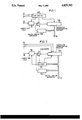
- FIG. 1 is schematic and block circuit diagram of an analog/digital converter according to the prior art.
- FIG. 2 is schematic and block circuit diagram of an analog/digital converter according to the invention.
- FIG. 1 there is seen a prior art analog/digital converter of the type mentioned above which includes a sample-and-hold element SH, a comparator K, a successive approximation register SAR, a digital/analog converter DAU and flow control means AST.
- the sampe-and-hold element SH is used for temporary storage of a voltage value located at an analog input AE during a conversion time, so that all of the digit places of the output word that is present at the data output DA after the conversion are formed by the same input voltage.
- the comparator K compares the measured value stored in the sample-and-hold element SH with the output voltage of the digital/analog converter DAU.
- the memory elements of the successive approximation register are preset, so that the digital output word at a data output DA of the successive approximation register SAR equals zero.
- the most significant bit is then set to a defined logical state, in particular a logical "1" potential, and monitored as to whether the input voltage or the output voltage of the sample-and-hold element SH is higher than the output voltage of the digital/analog converter DAU, which corresponds to the digital word of the successive approximation register. If this is the case, then it remains set; otherwise, it is erased. This weighing process is repeated for each bit until the least significant bit is also defined at the end of the conversion phase.
- the successive approximation register includes a shift register, in which the defined logical state is incremented by one position at each clock pulse.
- the bits are set empirically, in order, to the defined logical state.
- the result of a particular weighing process is also stored in memory elements, into which the applicable comparator state is read. Only the memory element having the associated bit which has just been tested, is made available in this process. Once the least significant bit has been defined, a further memory element of the shift register is typically set, in order to indicate that the conversion phase has been completed.
- the conversion and optional signal sampling and holding must be controlled and this is typically accomplished with the aid of the flow control means AST as shown in FIG. 1.
- the flow control means AST resets the starting and clock signal present at inputs ST and T for controlling the comparator K and the functions of the successive approximation register SAR and it optionally controls the sample-and-hold element SH.
- the flow control means AST usually requires a control counter with a decoder.
- FIG. 2 in which elements identical to those in FIG. 1 are provided with the same reference numerals.
- the successive approximation register SAR is triggered directly by starting or clock signals through the inputs ST and T.
- the analog/digital converter instead of specialized flow control means, has a decoder DS, the input side of which is connected to the data output DA and to the output of the successive approximation register SAR.
- the output side of the decoder DS controls the comparator K, the successive approximation register SAR itself, and optionally the sample-and-hold element SH.
- the decoder DS decodes the defined logical state that has been incremented upon each clock signal in the successive approximation register SAR and utilizes the result of the decoding for controlling the elements listed.
- a concrete embodiment of the decoder DS for controlling the functions of incrementing the defined logical state, writing in and storing the result of weighing on the part of the comparator in the successive approximation register SAR and on the part of the other two elements, can easily be provided by one of ordinary skill in the art.
Landscapes
- Engineering & Computer Science (AREA)
- Theoretical Computer Science (AREA)
- Analogue/Digital Conversion (AREA)
- Arrangements For Transmission Of Measured Signals (AREA)
Abstract
Description
Claims (4)
Applications Claiming Priority (2)
| Application Number | Priority Date | Filing Date | Title |
|---|---|---|---|
| DE3629830 | 1986-09-02 | ||
| DE3629830 | 1986-09-02 |
Publications (1)
| Publication Number | Publication Date |
|---|---|
| US4829302A true US4829302A (en) | 1989-05-09 |
Family
ID=6308740
Family Applications (1)
| Application Number | Title | Priority Date | Filing Date |
|---|---|---|---|
| US07/091,539 Expired - Lifetime US4829302A (en) | 1986-09-02 | 1987-08-31 | Analog/digital converter using the weighing method |
Country Status (5)
| Country | Link |
|---|---|
| US (1) | US4829302A (en) |
| EP (1) | EP0258841B1 (en) |
| JP (1) | JP2566205B2 (en) |
| AT (1) | ATE54392T1 (en) |
| DE (1) | DE3763553D1 (en) |
Cited By (13)
| Publication number | Priority date | Publication date | Assignee | Title |
|---|---|---|---|---|
| US4940982A (en) * | 1986-03-03 | 1990-07-10 | Zdzislaw Gulczynski | High speed integrating analog-to-digital converter |
| US5084704A (en) * | 1990-02-02 | 1992-01-28 | Grumman Aerospace Corporation | Focal plane analog-to-digital converter |
| US5200623A (en) * | 1991-12-04 | 1993-04-06 | Grumman Aerospace Corp. | Dual integration circuit |
| US5229770A (en) * | 1991-01-16 | 1993-07-20 | Mitsubishi Denki Kabushiki Kaisha | Analog/digital converter with advanced conversion termination notice |
| US5377248A (en) * | 1988-11-29 | 1994-12-27 | Brooks; David R. | Successive-approximation register |
| US5515050A (en) * | 1993-07-06 | 1996-05-07 | Advanced Micro Devices, Inc. | Apparatus and method for asynchronous successive approximation |
| US5859608A (en) * | 1995-09-29 | 1999-01-12 | Sgs-Thomson Microelectronics S.R.L. | Successive approximation and shift register without redundancy |
| US6094154A (en) * | 1998-01-13 | 2000-07-25 | Lg Semicon Co., Ltd. | Analog-to-digital converter |
| US6608582B2 (en) * | 2001-06-29 | 2003-08-19 | Intel Corporation | A/D conversion using a variable offset comparator |
| US6617926B2 (en) | 2001-06-29 | 2003-09-09 | Intel Corporation | Tail current node equalization for a variable offset amplifier |
| EP1443654A2 (en) * | 2003-01-29 | 2004-08-04 | EADS Deutschland GmbH | Method and circuit for converting an analogue actual value into a digital setpoint value |
| CN102571094A (en) * | 2010-12-10 | 2012-07-11 | 乐金显示有限公司 | Successive approximation register analog-to-digital converter and analog-to-digital conversion method using the same |
| US9906232B1 (en) * | 2017-03-10 | 2018-02-27 | Xilinx, Inc. | Resolution programmable SAR ADC |
Citations (3)
| Publication number | Priority date | Publication date | Assignee | Title |
|---|---|---|---|---|
| US4200863A (en) * | 1977-10-03 | 1980-04-29 | The Regents Of The University Of California | Weighted capacitor analog/digital converting apparatus and method |
| US4407020A (en) * | 1980-08-25 | 1983-09-27 | Trw Inc. | Automatic compensation circuit and method |
| US4460891A (en) * | 1982-06-03 | 1984-07-17 | Analog Devices, Incorporated | Analog-to-digital converter with explicit interpolation |
Family Cites Families (2)
| Publication number | Priority date | Publication date | Assignee | Title |
|---|---|---|---|---|
| JPS6013579B2 (en) * | 1978-04-21 | 1985-04-08 | 日本電信電話株式会社 | Companding AD converter |
| JPS5966741A (en) * | 1982-10-07 | 1984-04-16 | Omron Tateisi Electronics Co | Analog-digital converter |
-
1987
- 1987-08-28 DE DE8787112560T patent/DE3763553D1/en not_active Expired - Lifetime
- 1987-08-28 AT AT87112560T patent/ATE54392T1/en not_active IP Right Cessation
- 1987-08-28 EP EP87112560A patent/EP0258841B1/en not_active Expired - Lifetime
- 1987-08-31 US US07/091,539 patent/US4829302A/en not_active Expired - Lifetime
- 1987-09-01 JP JP62218991A patent/JP2566205B2/en not_active Expired - Fee Related
Patent Citations (3)
| Publication number | Priority date | Publication date | Assignee | Title |
|---|---|---|---|---|
| US4200863A (en) * | 1977-10-03 | 1980-04-29 | The Regents Of The University Of California | Weighted capacitor analog/digital converting apparatus and method |
| US4407020A (en) * | 1980-08-25 | 1983-09-27 | Trw Inc. | Automatic compensation circuit and method |
| US4460891A (en) * | 1982-06-03 | 1984-07-17 | Analog Devices, Incorporated | Analog-to-digital converter with explicit interpolation |
Non-Patent Citations (4)
| Title |
|---|
| Article by Jim Williams, EDN, 6/20/85, pp. 115 126. * |
| Article by Jim Williams, EDN, 6/20/85, pp. 115-126. |
| Research Notes, Int. J. Electronics, 1974, vol. 37, No. 5, pp. 711 713. * |
| Research Notes, Int. J. Electronics, 1974, vol. 37, No. 5, pp. 711-713. |
Cited By (17)
| Publication number | Priority date | Publication date | Assignee | Title |
|---|---|---|---|---|
| US4940982A (en) * | 1986-03-03 | 1990-07-10 | Zdzislaw Gulczynski | High speed integrating analog-to-digital converter |
| US5377248A (en) * | 1988-11-29 | 1994-12-27 | Brooks; David R. | Successive-approximation register |
| US5084704A (en) * | 1990-02-02 | 1992-01-28 | Grumman Aerospace Corporation | Focal plane analog-to-digital converter |
| US5229770A (en) * | 1991-01-16 | 1993-07-20 | Mitsubishi Denki Kabushiki Kaisha | Analog/digital converter with advanced conversion termination notice |
| US5200623A (en) * | 1991-12-04 | 1993-04-06 | Grumman Aerospace Corp. | Dual integration circuit |
| US5515050A (en) * | 1993-07-06 | 1996-05-07 | Advanced Micro Devices, Inc. | Apparatus and method for asynchronous successive approximation |
| US5859608A (en) * | 1995-09-29 | 1999-01-12 | Sgs-Thomson Microelectronics S.R.L. | Successive approximation and shift register without redundancy |
| US6094154A (en) * | 1998-01-13 | 2000-07-25 | Lg Semicon Co., Ltd. | Analog-to-digital converter |
| US6608582B2 (en) * | 2001-06-29 | 2003-08-19 | Intel Corporation | A/D conversion using a variable offset comparator |
| US6617926B2 (en) | 2001-06-29 | 2003-09-09 | Intel Corporation | Tail current node equalization for a variable offset amplifier |
| US20040021519A1 (en) * | 2001-06-29 | 2004-02-05 | Casper Bryan K. | Digitally controlled variable offset amplifier |
| US6798293B2 (en) | 2001-06-29 | 2004-09-28 | Intel Corporation | Digitally controlled variable offset amplifier |
| EP1443654A2 (en) * | 2003-01-29 | 2004-08-04 | EADS Deutschland GmbH | Method and circuit for converting an analogue actual value into a digital setpoint value |
| EP1443654A3 (en) * | 2003-01-29 | 2006-07-19 | EADS Deutschland GmbH | Method and circuit for converting an analogue actual value into a digital setpoint value |
| CN102571094A (en) * | 2010-12-10 | 2012-07-11 | 乐金显示有限公司 | Successive approximation register analog-to-digital converter and analog-to-digital conversion method using the same |
| CN102571094B (en) * | 2010-12-10 | 2014-11-26 | 乐金显示有限公司 | Successive approximation register analog-to-digital converter and analog-to-digital conversion method using the same |
| US9906232B1 (en) * | 2017-03-10 | 2018-02-27 | Xilinx, Inc. | Resolution programmable SAR ADC |
Also Published As
| Publication number | Publication date |
|---|---|
| JPS6364412A (en) | 1988-03-22 |
| EP0258841B1 (en) | 1990-07-04 |
| DE3763553D1 (en) | 1990-08-09 |
| EP0258841A1 (en) | 1988-03-09 |
| JP2566205B2 (en) | 1996-12-25 |
| ATE54392T1 (en) | 1990-07-15 |
Similar Documents
| Publication | Publication Date | Title |
|---|---|---|
| US4829302A (en) | Analog/digital converter using the weighing method | |
| US5307066A (en) | Microprocessor controlled converter having reduced noise interference and method of operating same | |
| US6456219B1 (en) | Analog-to-digital converter including two-wire interface circuit | |
| US5874911A (en) | Analog-to-digital converting circuitry | |
| KR900011161A (en) | Continuous Comparison Analog-to-Digital Converter | |
| US4852130A (en) | Successive approximation register | |
| US4999630A (en) | Fast analog-digital converter with parallel structure | |
| JP3268702B2 (en) | A / D converter | |
| EP0393716B1 (en) | Delay circuit | |
| US6215728B1 (en) | Data storage device capable of storing plural bits of data | |
| US4665382A (en) | Analog-to-digital conversion | |
| US4068229A (en) | High speed coding system for PCM signals with coarse and fine coding in an overlapping range | |
| US6414621B1 (en) | Analog to digital converter having a parallel converter and logic for generating serial data | |
| JP3298908B2 (en) | Analog-to-digital converter | |
| US5903144A (en) | Circuit configuration for phase difference measurement | |
| JP2555882B2 (en) | Signal processor | |
| JP2715656B2 (en) | Analog-to-digital converter | |
| SU443483A1 (en) | A spreading register for an analog-to-digital bit-balancing converter | |
| US6498579B2 (en) | Successive-approximation analog-digital converter and related operating method | |
| JPH02183628A (en) | Analog/digital converter | |
| SU864549A2 (en) | Follow-up analogue-digital converter | |
| KR950008484B1 (en) | A/d converter | |
| JPH0625785B2 (en) | Measuring device | |
| JPH0733174Y2 (en) | Digital data peak detection / readout circuit | |
| JP2002033661A (en) | Digital/analog converter circuit |
Legal Events
| Date | Code | Title | Description |
|---|---|---|---|
| AS | Assignment |
Owner name: SIEMENS AKTIENGESELLSCHAFT, GERMANY Free format text: ASSIGNMENT OF ASSIGNORS INTEREST.;ASSIGNORS:OITZL, ERICH;HAAS, MANFRED;REEL/FRAME:005027/0286 Effective date: 19870922 |
|
| STCF | Information on status: patent grant |
Free format text: PATENTED CASE |
|
| FEPP | Fee payment procedure |
Free format text: PAYOR NUMBER ASSIGNED (ORIGINAL EVENT CODE: ASPN); ENTITY STATUS OF PATENT OWNER: LARGE ENTITY |
|
| FPAY | Fee payment |
Year of fee payment: 4 |
|
| AS | Assignment |
Owner name: ESTEEM INTERNATIONAL, INC., MINNESOTA Free format text: ASSIGNMENT OF ASSIGNORS INTEREST;ASSIGNOR:MEREDIG, CATHERINE A.;REEL/FRAME:006696/0019 Effective date: 19930825 |
|
| FPAY | Fee payment |
Year of fee payment: 8 |
|
| FPAY | Fee payment |
Year of fee payment: 12 |